Article

Investigation of the Interfacial Reactions between the CoCuFeNi High Entropy Alloy and Sn Solder

1
Department of Materials Science and Engineering, National Taiwan University of Science and Technology, Taipei 10672, Taiwan
2
Department of Chemical Engineering, National Chung Cheng University, Chiayi 621301, Taiwan
*
Author to whom correspondence should be addressed.
Metals 2023, 13(4), 710; https://doi.org/10.3390/met13040710
Submission received: 6 March 2023 / Revised: 2 April 2023 / Accepted: 3 April 2023 / Published: 5 April 2023
(This article belongs to the Special Issue Feature Papers in Welding & Joining)

Abstract

:
The CoCuFeNi high entropy alloy (HEA) has excellent electrical, thermal, and mechanical properties. In electronic packaging technology, Sn is the major element of lead-free solders. In this study, we used the CoCuFeNi HEA as the substrate and Sn as the solder and investigated the liquid/solid interfacial reactions of the Sn/CoCuFeNi system at 300, 375, and 450 °C for 30, 60, 100, 150, 360, and 480 min. The results indicated that the (Fe, Co)Sn2 phase was formed in the Sn/CoCuFeNi couples for all various reaction temperatures and at different durations. Additionally, the (Co, Ni)Sn2 phase was precipitated at the solder side and near the (Fe, Co)Sn2 phase when the reaction time increased. The thickness of the (Fe, Co)Sn2 phase increased with the increase in reaction temperature and time, and it was proportional to the square root of the reaction time. Overall, our results showed that the growth mechanism of the (Fe, Co)Sn2 phase was diffusion-controlled in the Sn/CoCuFeNi couples.

1. Introduction

The lead frame in electronic packaging connects the integrated circuit to the surroundings and requires excellent electrical and thermal conductivity. Therefore, the material used for making lead frames must have good electrical conductivity, thermal conductivity, mechanical properties, and wettability [1]. High entropy alloys (HEAs) consist of different principal elements, and each component of the principal elements does not exceed 35% [2]. Therefore, the properties of each principal element are exhibited in the alloys through the cocktail effect and contribute to excellent electrical and thermal conductivity and mechanical properties [3]. If HEAs could be used as the lead frame materials, they might be able to overcome the limitations of conventional lead frame materials, such as limited mechanical strength, which can limit their ability to withstand stress and strain, especially in high-temperature and high-vibration environments. Therefore, enhancing the performance of the lead frame and increasing the possibility of applying HEAs in electronic packaging is beneficial. In addition, during the usage of electronic products, they undergo varying electronic aging conditions due to different usage methods. Therefore, reliability analysis tests are essential. In the thermal aging experiment, an intermetallic compound (IMC) is generated at the interface due to the contact and mutual diffusion between the two metals. Research has shown that the generation of a relatively thick IMC phase not only makes the solder joint more prone to brittle fracture, but also significantly increases the risk of failure due to the thermal expansion mismatch (Misfit) between the solder and the substrate, resulting in a significant decrease in product reliability. Therefore, the growth behavior of the IMC layer generated at the interface in the solder joint during long-term use of the product also needs to be closely monitored.
Liu et al. reported that the CoCuFeNi HEA has a single face-centered cubic (FCC) lattice structure [4]. The results of their study also showed that the FCC structure in the CoCuFeNi HEA has excellent mechanical properties [5]. The CoCuFeNi HEA had excellent electrical and thermal conductivity because it contained Cu and Fe, which have good electrical and thermal conductivity. For the development and application of new technology, the performance of lead frame materials needs to be considerably improved, such as alloys with high strength, as well as electrical and thermal conductivity. For example, compared with pure Cu, which was commonly used earlier as a lead frame material in electronic packaging, Cu-based HEAs have better mechanical, electrical and thermal properties. Thus, these alloys were extensively used to produce HEAs [6]. Additionally, Cu, as the principal element in the CoCuFeNi HEA, plays an important role in the soldering. It has excellent wettability and reactivity with Sn-based solders. Thus, adding Cu to the CoCuFeNi HEA might significantly improve its wettability and reactivity with the Sn-based solder [7]. Overall, the CoCuFeNi HEA has a high potential to be used as a lead frame material in electronic packaging. Sn is the principle element of lead-free solders [8]. A few studies investigated the interfacial reactions between HEA and Sn. The study by Li et al. on the interfacial reaction between CoCuFeNi HEA and Sn at 250 °C for 2, 6, 12, and 24 h showed that the (Fe, Co)Sn2 phase was formed at the Sn/CoCuFeNi interface, and the thickness of the (Fe, Co)Sn2 phase was increased with the increase in reaction times and temperatures [9]. Ma et al. reported that the CuFeCoNiCr HEA reacted with Sn at 450 °C to form the Cu6Sn5 and Cu3Sn phases at the interface [10]. The findings of these studies on the interfacial reactions between the HEA and Sn were related to the reaction temperatures and times, and the interface showed the interdiffusion of atoms and the formation of intermetallic compounds (IMCs).
In this study, we systematically investigated the liquid/solid interfacial reactions at 300, 375, and 450 °C between CoCuFeNi HEA and Sn. In addition, IMCs formed at the interface were identified, and their morphologies, thicknesses, and growth mechanism were analyzed. Our findings might help in evaluating the feasibility of using CoCuFeNi HEA as a desirable lead frame material in electronic packaging.

2. Materials and Methods

The CoCuFeNi high entropy alloy (HEA) was prepared with pure elements, including Co (99.9+ wt.%, SEED CHEM; Camberwell, VIC, Australia), Cu (99.9+ wt.%, Alfa Aesar; Haverhill, MA, USA), Fe (99.9+ wt.%, Alfa Aesar; Haverhill, MA, USA), and Ni (99.9+ wt.%, Alfa Aesar; Haverhill, MA, USA). The pure elements were accurately weighed, and the composition of these four principal elements was maintained at 25 at.% (total weight: 3 g). Then, the pure elements were placed in a Cu crucible in an arc melting furnace (Miller, Gold Star 602; Appleton, WI, USA), and a piece of Ti was placed in the small depression on the other side of the crucible for striking. After the crucible was placed inside the arc melting furnace, the chamber of the arc melting furnace was purged with Ar gas to reduce the possible oxidation of the alloys, and the current of the arc melting furnace was adjusted to 200 A. The metal elements were arc melted together and CoCuFeNi HEA ingot was formed. The ingot alloy was flipped upside down and remelted in the arc melter at least five times to ensure homogeneous mixing of each element. After the arc melting was over, the ingot alloy was removed from the arc melting furnace and weighted again to make sure there was no weight loss, and its dimension was approximately a circular disc with a diameter of 10 mm. Then, the ingot alloy was encapsulated in a quartz tube in a vacuum environment (2 × 10⁻³ N/m2), and the tube was placed in a furnace at 1000 °C for 24 h to homogenize the ingot alloy. After homogenization, the tube was quenched in icy water. The homogenized CoCuFeNi high entropy alloys were cut into discs (6.0 mm in diameter and 2.0 mm in thickness) using a cutting machine (Buehler, Isomet M30; Wooster, OH, USA), and then they were processed for metallographic treatment, including grinding and polishing. The disc of the CoCuFeNi HEA was dipped with flux (α-100, Alpha; South Plainfield, NJ, USA) on both sides. Sn (99.8+ wt.%, Alfa Aesar; Haverhill, MA, USA) and CoCuFeNi HEA were then encapsulated in a quartz tube under a pressure of 2 × 10⁻³ N/m2 and then placed inside an oven at different temperatures (300, 375, and 450 °C) to form a liquid/solid Sn/CoCuFeNi couple. The reaction duration was 30, 60, 100, 150, 360, and 480 min. The CoCuFeNi HEA-to-Sn ratio (by weight) was 1:3, and the Sn and HEA encapsulated in a quartz tube were placed by first placing the high-entropy alloy into the tube with pliers, and then placing the Sn behind the high-entropy alloy to enclose it.
After the reaction, each couple was quenched in icy water. Then, each couple was put in a hot mounting machine (Simpliment 1000, Buehler; Wooster, OH, USA) for mounting. These couples were carefully processed for metallographic treatment, including grinding and polishing to obtain smooth interfaces for further observation and analysis. The surface morphology and the surface of metallographic cuts of the couple were examined using a scanning electron microscope (SEM; Hitachi, TM-3000; Tokyo, Japan) to determine whether a new phase was generated at the interface. An SEM with energy-dispersive spectrometer (EDS; Bruker, Quantax 70; Billerica, Berlin, Germany) was used to perform the quantitative analysis and determine the composition of the particles. An X-ray Powder Diffractometer (XRD; Bruker, 2 PHASER XE-T XRD; Berlin, Germany) was used to conduct a diffraction analysis, and it was also performed at the interface to identify the types of IMC phases generated at the interface and to check the results obtained from EDS. An image software (ImageJ) was used to measure the area and the length of the IMC in the SEM image. Then, the area was divided by the length of the selected region to obtain the average thickness of the IMC. Each couple was measured three times, and the average thickness of the IMC was recorded to ensure accurate measurements.

3. Results

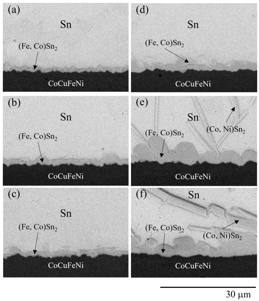
3.1. Interfacial Reactions in the Sn/CoCuFeNi Couples at 300 °C

The back-scattered electron image (BEI) of the Sn/CoCuFeNi couple that was reacted at 300 °C for 30 min is shown in Figure 1a. The darker region at the bottom in Figure 1a was the CoCuFeNi HEA, whereas the bright region at the top in Figure 1a was the Sn solder. When two different metals come into contact at a fixed temperature, the chemical potential difference between the atoms can cause an increase in the atomic Gibbs free energy at the interface. The atoms would diffuse across the interface to achieve a stable equilibrium state and lower the Gibbs free energy. If the concentration gradient changes discontinuously during the diffusion process, a new second phase may be generated at the interface, which is called an intermetallic compound (IMC). Therefore, a gray layer between the CoCuFeNi HEA and Sn solder was observed. It had a unique composition of Fe-6.8Co-63.8Sn (in at.%) with minor amounts of Ni and Cu, as determined by SEM/EDS analysis. This layer should be (Fe, Co)Sn2, which was determined by the Hume-Rothery substitutional solid solution rules [11] and the Fe-Sn phase diagram [12], which will be discussed in the discussion section. The BEI micrographs of the Sn/CoCuFeNi couple reacted at 300 °C for 60 to 480 min are shown in Figure 1b–f. Only the (Fe, Co)Sn2 phase was formed at the interface, and the EDS analysis results of the IMC at 375 °C are listed in Table 1. This result revealed that increasing the reaction time would not change the IMC formation in the Sn/CoCuFeNi couple. However, the thickness of the (Fe, Co)Sn2 phase increased with the increase in the reaction times. The thickness of the (Fe, Co)Sn2 phase increased from 0.96 μm after 30 min of reacting to 2.95 μm after 480 min of reacting. As shown in Figure 1f, another precipitated phase was formed on the solder, when the Sn/CoCuFeNi couple was reacted at 300 °C for 480 min. This phase had a unique composition of Co-13.2Ni-67.8Sn (in at.%) with minor solubility of the Fe and Cu atoms. From the Co-Sn phase diagram [13] and the Hume-Rothery substitutional solid solution rules [11], which will be discussed in the discussion section, we found that this precipitated phase should be the (Co, Ni)Sn2 phase.

3.2. Interfacial Reactions in the Sn/CoCuFeNi Couples at 375 °C

Figure 2a shows the BEI micrograph of the Sn/CoCuFeNi couple reacted at 375 °C for 30 min. Similar to the Sn/CoCuFeNi couple that was reacted at 300 °C, the gray layer between the CoCuFeNi HEA and the Sn solder was found and it had a unique composition of Fe-8.7Co-65.2Sn (in at.%) with minor amounts of Ni and Cu, as determined by SEM/EDS analysis. This layer should be the (Fe, Co)Sn2, which was determined by the Fe-Sn phase diagram [12] and the Hume-Rothery substitutional solid solution rules [11]. The BEI micrographs of the Sn/CoCuFeNi couple reacted at 375 °C for 60 to 480 min are shown in Figure 2b–f. Only the (Fe, Co)Sn2 phase was formed at the interface.
The thickness of the IMC in the Sn/CoCuFeNi couples conducted for different periods (30–480 min) became thicker as the reaction time increased. The IMC thickness increased from 1.39 μm after 30 min of reaction to 5.2 μm after 480 min of reaction. The results showed that the IMC was similar to that formed in the Sn/CoCuFeNi couple reacted at 300 °C, but became thicker as the reaction temperature increased, and it was also more obvious between the Sn solder and CoCuFeNi HEA alloy. The BEI micrographs of the Sn/CoCuFeNi couples reacted at 375 °C for 360 and 480 min are shown in Figure 2e–f, and the EDS analysis results of the IMC at 375 °C are listed in Table 1. The precipitated phases were formed on the solder side after the reactions were conducted for 360 and 480 min, and they had compositions of Co-8.3Ni-70.4Sn (in at.%) and Co-9.2Ni-69.2Sn (in at.%) with minor solubility of Fe and Cu atoms, respectively. Based on the Co-Sn phase diagram [13] and the Hume-Rothery substitutional solid solution rules [11], these precipitated phases should be the (Co, Ni)Sn2.

3.3. Interfacial Reactions in the Sn/CoCuFeNi Couples at 450 °C

Figure 3a shows the BEI micrograph of the Sn/CoCuFeNi couple reacted at 450 °C for 30 min. Similar to the couples that reacted at 300 and 375 °C, only the gray layer between the CoCuFeNi HEA and the Sn solder was found. It also had a unique composition of Fe-4.3Co-65.9Sn (in at.%) with minor solubility of Ni and Cu atoms, as determined by SEM/EDS analysis. This layer should be the (Fe, Co)Sn2 phase, which was determined by the Fe-Sn phase diagram [12] and the Hume-Rothery substitutional solid solution rules [11]. When the BEI micrographs of the Sn/CoCuFeNi couple reacted at 450 °C for 60 to 480 min, only the (Fe, Co)Sn2 phase was formed at the Sn/CoCuFeNi interface, as shown in Figure 3b–f, and the EDS analysis results of the IMC at 450 °C are listed in Table 1.
In the BEI images for the reactions conducted for 30 to 480 min, we found that the IMCs were thickened when the aging time was increased. The thickness of the IMC increased from 3.27 μm after 30 min of reaction to 52.84 μm after 480 min of reaction. Overall, the results revealed that the thickness of the IMC increased with the increase in reaction time and temperature. The BEI micrographs of the Sn/CoCuFeNi couple reacted at 450 °C for 150, 360, and 480 min are shown in Figure 3d–f. Similar to the couples reacted at 300 and 375 °C, the precipitated phase of the (Co, Ni)Sn2 phase was on the solder side. Increasing the reaction temperature would enhance the diffusion and dissolution rates of Co toward the molten solder. In this case, the (Co, Ni)Sn2 phase was formed after the Sn/CoCuFeNi couple reacted at 450 °C for 150 min.
In addition, to identify the IMC generated at the interface, X-ray diffraction (XRD) analysis was also performed on the interface of the Sn/CoCuFeNi couple reacted at 450 °C for 30 and 600 min in this experiment. The results showed that the FeSn2 phase was still the main phase structure at the interface of the IMC after the long-term reaction, and the peak intensity of FeSn2 increased with the increase in the reaction time. This indicates that the crystallinity of the FeSn2 phase is relatively significant over a long period, as shown in Figure 4.

4. Discussion

4.1. IMC in the CoCuFeNi/Sn Couple

According to the Hume-Rothery substitutional solid solution rules, when the atomic radius of the solute and solvent atoms differs by less than 14 to 15%, the formation of the solid solutions with greater solid solubility is favored, i.e., atoms can replace each other [11]. The atomic radii of Fe and Co atoms were 0.126 and 0.125 nm, respectively. The difference in the size between the two atoms is considerably smaller than the threshold of 14 to 15% proposed by the Hume-Rothery rule. Thus, Fe atoms and Co atoms substituted each other in this case. Additionally, with the composition of the layer in the Sn/CoCuFeNi system, the sum of composition of (Fe + Co) and Sn corresponded to the position of the FeSn2 in the Fe-Sn phase diagram [12]. Therefore, the IMC layer in the Sn/CoCuFeNi couples reacted at 300, 375, and 450 °C for 30 min is likely to be the FeSn2 phase, and it is marked as the (Fe, Co)Sn2 phase. When the reaction times were increased from 60 to 480 min, only the (Fe, Co)Sn2 phase was formed at the interface in the Sn/CoCuFeNi couples reacted at 300, 375, and 450 °C, as shown in Figure 1b–f and Figure 3b–f. This result revealed that increasing the reaction time and temperature would not change the IMC formation in the Sn/CoCuFeNi couple reacted at 300, 375, and 450 °C.
However, Li et al. conducted an interfacial reaction between the CoCuFeNi HEA and Sn solder reacted at 250 °C for 2, 6, 12, and 24 h [9]. Their results showed that only the (Fe, Co)Sn2 phase was formed at 250 °C in the Sn/CoCuFeNi system. They also reported that the IMC became thicker as the reaction time increased [9]. The findings of the study by Li et al. on the interfacial reaction between the CoCuFeNi HEA and Sn solders was constructed with those of our study on the Sn/CoCuFeNi system. Moreover, Li et al.’s study results also revealed that the IMC thickness thickened as the aging time prolonged; this result corresponded to the IMC growth results in this study. Therefore, the interface reaction in this present study, the IMC at the interface, was mainly composed of Fe atoms diffusing toward the solder side, which reacted with Sn to form the (Fe, Co)Sn2 phase.
Nevertheless, we also had new findings different from those in the previous study by Li et al. [9], and we found that there was another precipitated phase, which was the (Co, Ni)Sn2 phase, which was formed on the solder after the Sn/CoCuFeNi couple was reacted at a higher temperature and a longer time reaction. When the reaction temperature was increased, it would accelerate the diffusion rate of Co and Ni diffused from the CoCuFeNi HEA toward the molten solder. Meanwhile, more Co and Ni atoms dissolved into the molten solder, causing the (Co, Ni)Sn2 phase to be formed in the Sn/CoCuFeNi couple that, after, reacted at 300 °C for 480 min, 375 °C for 360 min, and 450 °C for 150 min, as shown in Figure 1, Figure 2 and Figure 3.

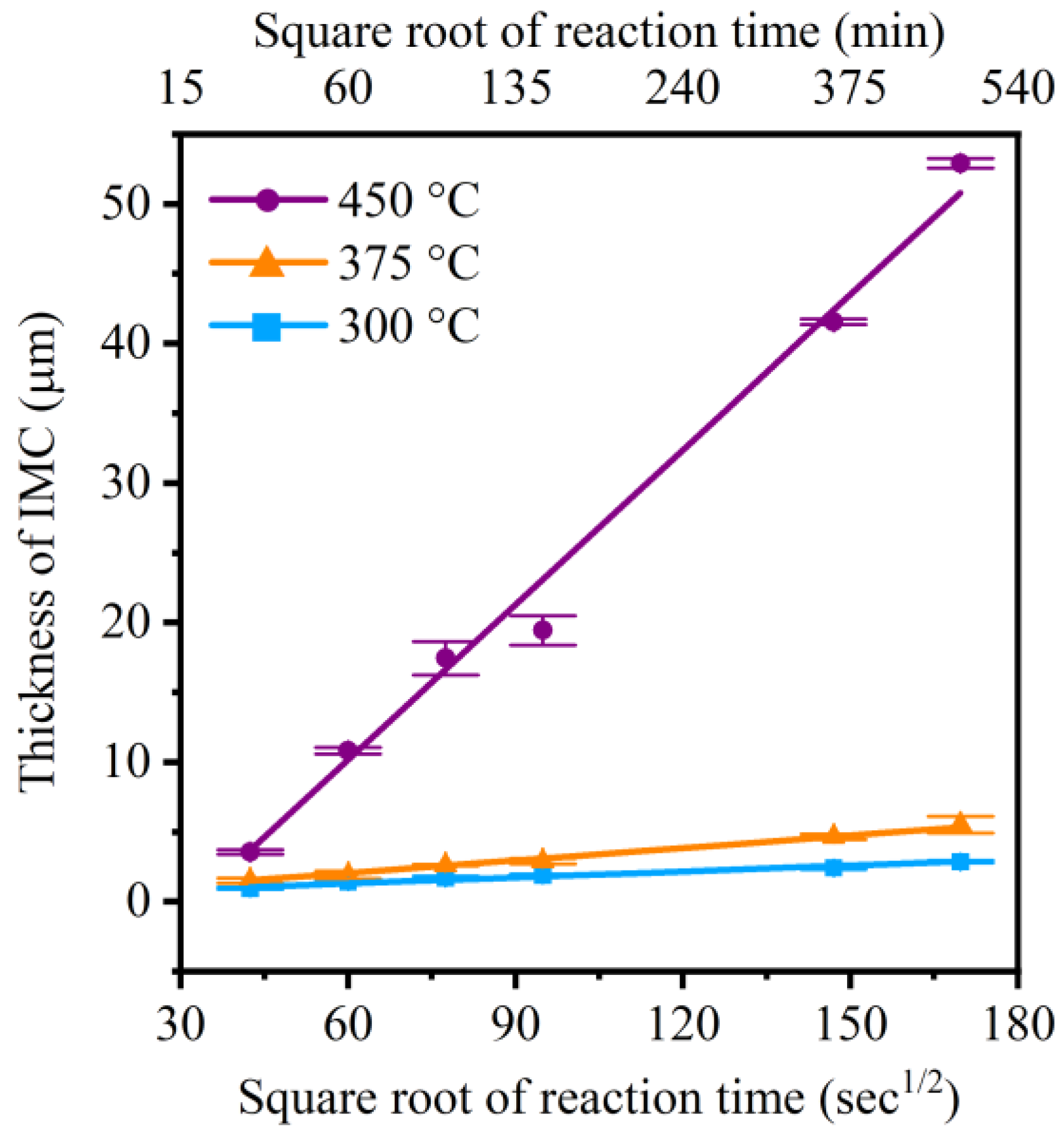
4.2. Reaction Kinetics in the CoCuFeNi/Sn Couple

To further investigate the thickness and the growth mechanism of the IMC, its thickness and the square root of the reaction time was plotted in Figure 5. It illustrated the relationship between the total IMC thickness and the square root of the reaction time in the Sn/CoCuFeNi system. The three straight lines in Figure 5 are the growth curve for the Sn/CoCuFeNi couple reacted at 300, 375, and 450 °C; the curves follow the parabolic law. The growth of the IMC is controlled by various mechanisms, such as the diffusion of reacting elements and the rate of reaction, and this can be predicted by the growth curve in Figure 5. If the growth curve is parabolic, the IMC growth is controlled by the rate of reaction, and if growth curve is a straight line, then the diffusion of the reacting element is the diffusion-controlled mechanism.
This indicates that the IMC growth mechanism in the Sn/CoCuFeNi couple is diffusion-controlled. Kumar et al. found that the growth of an IMC layer can be represented by the following empirical power law [14]:
x = (k × t)1/2,
where x indicates the thickness of the IMC, t indicates the reaction time, and k indicates the growth rate constant. The growth rate constant (k) represents the overall growth rate of the IMC, so we used this empirical power law to calculate the growth rate constant (k) of the IMC in the Sn/CoCuFeNi couple at 300, 375, and 450 °C. The corresponding values are listed in Table 2.
The results showed that an increase in the reaction temperature increased the rate of growth of the IMC growth rate in the Sn/CoCuFeNi couple and increased the k values. Therefore, the IMC was thicker at a higher reaction temperature than that at the lower reaction temperature for the same reaction time. Finally, based on the study by Li et al. and the variation in the growth rate constant (k) with temperature, we used the Arrhenius empirical equation [15]:
k = k0[exp(−Q/RT)],
where k is the IMC growth constant, k0 is the frequency factor, Q indicates activation energy, and R indicates the gas constant (8.414 J/mol-K), to calculate the activation energy (Q). The plot of the natural logarithm of k (ln k) as a function of the inverse temperature (1/T) is showed in Figure 6, and the slope of this plot was −Q/R. Therefore, the value Q for the Sn/CoCuFeNi couple was found to be 108 kJ/mol.

5. Conclusions

In this study, we investigated the formation and thickness of the IMC and the IMC growth mechanism and growth constant under different reaction temperatures and durations in the CoCuFeNi/Sn couple. For the reaction conducted at 300, 375, and 450 °C, only the (Fe, Co)Sn2 phase was formed in the CoCuFeNi/Sn couple. The XRD analysis results also identified that the main phase structure generated at the interface was still FeSn2. However, (Co, Ni)Sn2 was precipitated by phases that were formed on the solder side and near the (Fe, Co)Sn2 phase when the reaction time was 360 and 480 min. The thickness of the IMC increased with the increase in reaction time and temperature. The IMC thickness obeyed the parabola law. Thus, the IMC growth mechanism was diffusion-controlled. Finally, the results indicated that the increase in the reaction temperature increased the growth rate (k) of the IMC in all couples. The activation energy (Q) value was 108 kJ/mol in the Sn/CoCuFeNi couple. In the future, we will perform thermal and electrical conductivity tests to study the IMC’s thermal and electrical conductivity. In addition, we will also add more Cu to the CoFeNiCu HEA, such as CoFeNiCu2 HEA to investigate the diffusion behavior of the Cu between the HEA and solder in the next research.

Author Contributions

Conceptualization: Y.-W.Y.; formal analysis: T.-Y.C.; investigation: T.-Y.C. and Y.-C.C.; methodology: Y.-W.Y.; project administration: Y.-W.Y.; supervision: Y.-W.Y.; writing—original draft: T.-Y.C.; writing—review and editing: T.-Y.C., C.-H.W., A.D.L., and Y.-W.Y. All authors have read and agreed to the published version of the manuscript.

Funding

This research was funded by the National Science and Technology Council, Taiwan, R.O.C. (grant number NSTC111-2813-C-011-012-E and MOST 111-221-E-011-110-MY3).

Institutional Review Board Statement

Not applicable.

Informed Consent Statement

Not applicable.

Data Availability Statement

Not applicable.

Acknowledgments

The authors are also thankful for the help from S.C. Liaw, who works at the National Taiwan University of Science and Technology, for SEM-EDS operation.

Conflicts of Interest

The authors declare no conflict of interest.

References

  1. Breedis, J.F.; Chia, P.Y.; Goh, Y.G. Encyclopedia of Materials: Science and Technology, 1st ed.; Buschow, K.H.J., Ed.; Elsevier Science Ltd.: Houston, TX, USA, 2001; pp. 2683–2688. [Google Scholar]
  2. Yeh, J.W.; Chen, S.K.; Lin, S.J.; Gan, J.Y.; Chin, T.S.; Shun, T.T.; Tsau, C.H.; Chang, S.Y. Nanostructured High-Entropy Alloys with Multiple Principal Elements: Novel Alloy Design Concepts and Outcomes. Adv. Eng. Mater. 2004, 6, 299–303. [Google Scholar] [CrossRef]
  3. Zhang, J.; Zhu, H.; Xie, Z. Effects of Y and Al additions on the microstructure and tensile properties of CoCr3Fe5Ni high entropy alloys. Mater. Lett. 2021, 299, 130110–130114. [Google Scholar] [CrossRef]
  4. Liu, L.; Zhu, J.B.; Zhang, C.; Li, J.C.; Jiang, Q. Microstructure and the properties of FeCoCuNiSnx high entropy alloys. Mater. Sci. Eng. A 2012, 548, 64–68. [Google Scholar] [CrossRef]
  5. Ma, H.; Shao, Y.; Shek, C.H. CoCuFeNi high entropy alloy reinforced by in-situ W particles. Mater. Sci. Eng. A 2020, 797, 140218–140226. [Google Scholar] [CrossRef]
  6. Geng, Y.; Ban, Y.; Wang, B.; Li, X.; Song, K.; Zhang, Y.; Jia, Y.; Tian, B.; Liu, Y.; Volinsky, A. A review of microstructure and texture evolution with nanoscale precipitates for copper alloys. J. Mater. Res. Technol. 2020, 9, 11918–11934. [Google Scholar] [CrossRef]
  7. Shen, Y.A.; Yang, X.M.; Tsai, C.Y.; Ouyang, Y.H.; Tsai, M.H.; Shun, T.T. Effect of Cu on the interfacial reaction between Sn-based solders and FeCoNiCu alloys. Intermetallics 2022, 144, 107530–107535. [Google Scholar] [CrossRef]
  8. Xu, K.K.; Zhang, L.; Jiang, N. Effect of CNTs on the intermetallic compound growth between Sn solder and Cu substrate during aging and reflowing. Mater. Electron. 2021, 32, 2655–2666. [Google Scholar] [CrossRef]
  9. Li, Y.H. Investigation and Evaluation on Interfacial Reactions of High-Entropy Alloys with Lead-Free Solders. Master’s Thesis, Department of Chemical Engineering National Chung Cheng University, Chia-yi County, Taiwan, 2021. [Google Scholar]
  10. Ma, G.F.; Li, Z.K.; Ye, H.; He, C.L.; Zhang, H.F.; Hu, Z.Q. Wetting and interface phenomena in the molten Sn/CuFeNiCoCr high-entropy alloy system. Appl. Surf. Sci. 2015, 356, 460–466. [Google Scholar] [CrossRef]
  11. Ren, M.X.; Li, B.S.; Fu, H.Z. Formation condition of solid solution type high-entropy alloy. Trans. Nonferrous Met. Soc. China 2013, 23, 991–995. [Google Scholar] [CrossRef]
  12. Okamoto, H. Phase Diagram of Binary Iron Alloys, 2nd ed.; ASM International: Novelty, OH, USA, 1993; pp. 85–392. [Google Scholar]
  13. Jedličková, V.; Zemanová, A.; Kroupa, A. The Thermodynamic Assessment of the Co-Sn System. J. Phase Equilib. Diffus. 2019, 40, 21–33. [Google Scholar] [CrossRef]
  14. Kumar, A.; Chen, Z. Interdependent Intermetallic Compound Growth in an Electroless Ni-P/Sn-3.5Ag Reaction Couple. J. Electron. Mater. 2011, 40, 213–223. [Google Scholar] [CrossRef]
  15. Li, Y.C.; Chang, C.H.; Pasana, A.S.; Hsiao, H.M.; Yen, Y.W. Interfacial Reactions in Lead-Free Solder/Cu-2.0Be (Alloy 25) Couples. J. Electron. Mater. 2021, 50, 903–913. [Google Scholar] [CrossRef]
Figure 1. BEI micrographs of the Sn/CoCuFeNi couples reacted at 300 °C for (a) 30, (b) 60, (c) 100, (d) 150, (e) 360, and (f) 480 min.
Metals 13 00710 g001
Figure 2. BEI micrographs of the Sn/CoCuFeNi couples reacted at 375 °C for (a) 30, (b) 60, (c) 100, (d) 150, (e) 360, and (f) 480 min.
Metals 13 00710 g002
Figure 3. BEI micrographs of the Sn/CoCuFeNi couples reacted at 450 °C for (a) 30, (b) 60, (c) 100, (d) 150, (e) 360, and (f) 480 min.
Metals 13 00710 g003
Figure 4. The XRD diffraction patterns of the Sn/CoCuFeNi couple reacted at 450 °C for 30 and 600 min.
Metals 13 00710 g004
Figure 5. Plot of the thickness of IMC versus reacted at times and temperatures in the Sn/CoCuFeNi couples.
Metals 13 00710 g005
Figure 6. The Arrhenius plot of ln(k) vs. 1/T for the Sn/CoCuFeNi couple.
Metals 13 00710 g006
Table 1. EDS analysis results of the IMC in the Sn/CoCuFeNi couples.
TemperatureTime
(min)
Co
(at.%)
Cu
(at.%)
Fe
(at.%)
Ni
(at.%)
Sn
(at.%)
300 °C306.82.624.72.163.8
604.55.426.11.365.8
1006.81.425.72.263.9
15011.90.825.54.457.4
3609.70.624.32.762.7
48012.50.319.83.064.3
375 °C308.72.917.65.765.2
608.93.321.24.262.5
10018.03.716.16.359.1
15011.72.820.15.160.3
36014.02.412.35.363.3
48016.82.913.75.561.2
450 °C304.30.228.80.865.9
605.90.026.02.265.8
10010.10.420.81.966.8
15011.60.419.02.866.2
36014.50.013.05.267.3
48015.80.914.63.165.6
Table 2. The growth rate constant (k) of the IMC and reaction activation energy (Q) for the Sn/CoCuFeNi couple.
SystemGrowth Rate Constant k (×1016 m2/s)Q
(KJ/mole)
300 °C375 °C450 °C
Sn/CoCuFeNi4.210.1540108
Disclaimer/Publisher’s Note: The statements, opinions and data contained in all publications are solely those of the individual author(s) and contributor(s) and not of MDPI and/or the editor(s). MDPI and/or the editor(s) disclaim responsibility for any injury to people or property resulting from any ideas, methods, instructions or products referred to in the content.

