Article

Combined Effect of Substrate Temperature and Sputtering Power on Phase Evolution and Mechanical Properties of Ta Hard Coatings

1
Chaozhou Branch of Chemistry and Chemical Engineering Guangdong Laboratory, Chaozhou 521000, China
2
State Key Laboratory of Advanced Technology for Materials Synthesis and Processing, Wuhan University of Technology, Wuhan 430070, China
3
Hubei Key Laboratory of Advanced Technology for Automotive Components, Wuhan University of Technology, Wuhan 430070, China
*
Author to whom correspondence should be addressed.
Metals 2023, 13(3), 583; https://doi.org/10.3390/met13030583
Submission received: 23 February 2023 / Revised: 10 March 2023 / Accepted: 11 March 2023 / Published: 13 March 2023
(This article belongs to the Topic Microstructure and Properties in Metals and Alloys)

Abstract

:
Ta hard coatings were prepared on PCrNi1MoA steel substrates by direct current magnetron sputtering, and their growth and phase evolution could be controlled by adjusting the substrate temperature (Tsub) and sputtering power (Pspu) at various conditions (Tsub = 200–400 °C, Pspu = 100–175 W). The combined effect of Tsub and Pspu on the crystalline phase, surface morphology, and mechanical properties of the coatings was investigated. It was found that higher Pspu was required in order to obtain α-Ta coatings when the coatings are deposited at lower Tsub, and vice versa, because the deposition energy (controlled by Tsub and Pspu simultaneously) within a certain range was necessary. At the optimum Tsub with the corresponding Pspu of 200 °C-175 W, 300 °C-150 W, and 400 °C-100 W, respectively, the single-phased and homogeneous α-Ta coatings were obtained. Moreover, the α-Ta coating deposited at Tsub-Pspu of 400 °C-100 W showed a denser surface and a finer grain, and as a result exhibited higher hardness (9 GPa), better toughness, and larger adhesion (18.46 N).

1. Introduction

Protective coatings with excellent properties, such as high strength, toughness, good wear, and ablation resistance, are essential materials to ensure long-term, stable, and safe service for key artifacts applied in extreme service environments. The widely used Cr plating has a high melting point and large hardness to mitigate ablation and wear at high temperatures. However, the Cr plating is brittle and often cracks, leading to limited protection of artifacts [1,2,3]. In this case, a series of new ablation-resistant materials, including alloys and ceramics [4,5], have been developed. Among them, Ta coating is considered to be an alternative material to Cr plating because of its higher melting point, more excellent anti-ablation ability, and better toughness [6,7].
It should be noted that Ta coatings display two crystalline phases with entirely distinct characteristics: the stable α-Ta (Im3m space group, a = 3.304 Å) with a body-centered cubic crystal lattice structure, which has a high melting temperature (2996 °C), moderate hardness (8–12 GPa), and good toughness, and the metastable β-Ta (P421m space group, a = 5.313 Å, c = 10.194 Å) with a tetragonal crystal lattice structure, which is harder (18–20 GPa) but brittle and thermally unstable over 700 °C [8,9,10]. Magnetron sputtering is commonly used to prepare Ta coatings. Unfortunately, β-Ta always nucleates priorly using this method, which is unsuitable for protective materials. Therefore, many studies have attempted to regulate the phase formation of Ta coatings by adjusting the sputtering conditions, including substrate temperature [11], sputtering power [12], pressure [13], and post treatments [14], etc. Nevertheless, investigations on the phase formation in Ta coatings have yielded some conflicting results. For example, some studies [15] reported that a higher substrate temperature exceeding 365–375 °C was needed to promote α-Ta formation against β-Ta formation. On the contrary, recent experiments showed that pure α-Ta coatings could be fabricated even at a lower temperature of 200 °C [8]. The deposition energy is believed to be the most important factor determining the structural evolution of the coatings. An “energy window” was thus proposed, where α-Ta coatings could be formed between a specific energy range, while other energies higher or lower than this range would be beneficial to β-Ta coatings [16]. For magnetron sputtering, the substrate temperature [11] and sputtering power [12] are typically regarded as two important process variables concerned with the deposition energy, which can affect the surface activity of the substrate and the mobility of deposited Ta particles at the same time. The effects of substrate temperature [11] or sputtering power [12] on the preparation of Ta coatings have been investigated separately; however, their combined effect on the growth and phase evolution of Ta hard coatings has not yet been reported.
In this work, we conducted a comprehensive investigation on the structural evolution of Ta coatings using direct current magnetron sputtering by adjusting the substrate temperature (Tsub) and sputtering power (Pspu) simultaneously. The combined effect of Tsub and Pspu is discussed and the relationship between phase structure, surface morphology, mechanical properties, and the deposition parameters are established, to obtain single-phased α-Ta coatings with a fine structure and good mechanical properties.

2. Experimental Procedure

2.1. Preparation

2.1.1. Substrate Pretreatment

PCrNi1MoA steels (10 × 10 × 1 mm3 in size) were used as substrates. The substrates were mechanically ground using sandpaper from P240 up to P2000 and then polished by diamond suspension from 3 μm to 1 μm. The polished substrates were ultrasonically cleaned in acetone for 15 min and then dried with cold air. The chemical compositions of the alloy steel are shown in Table 1.

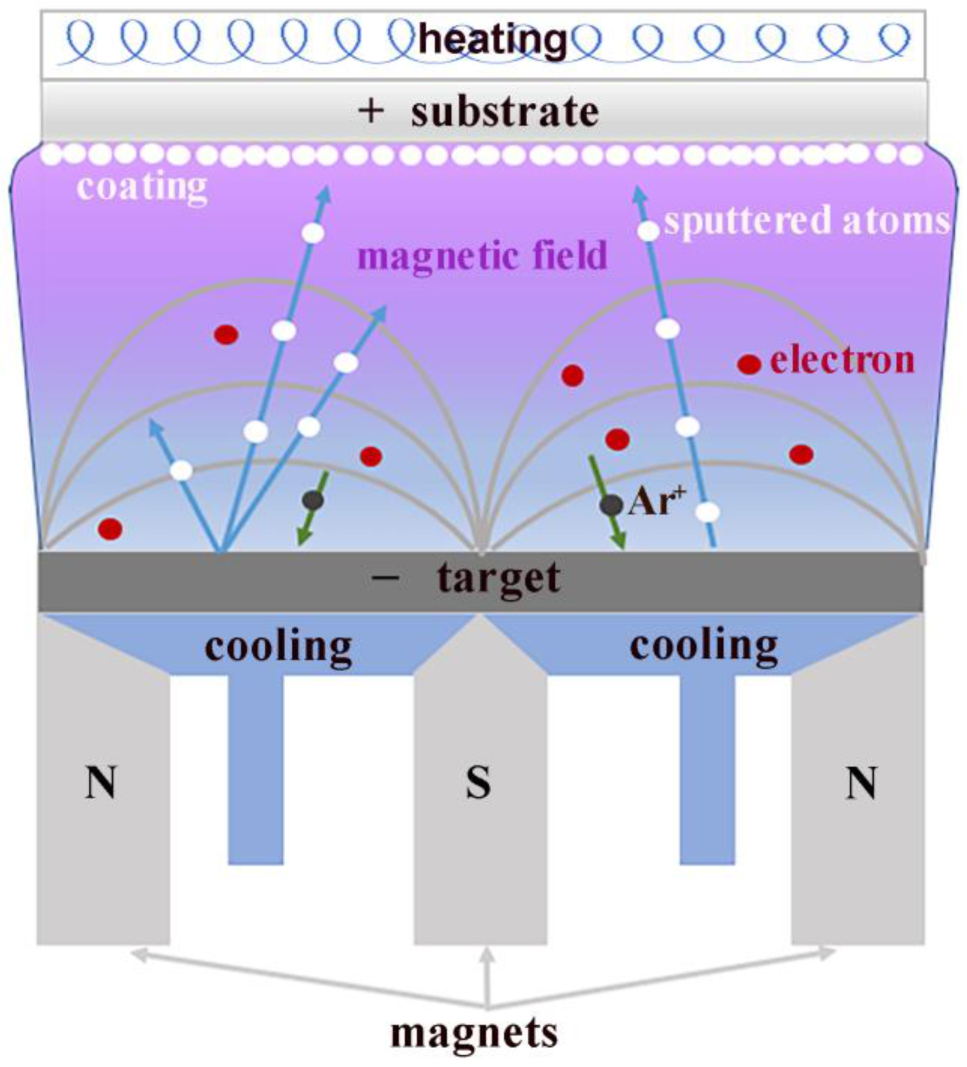
2.1.2. Deposition Device

This experiment adopts DC magnetron sputtering (DCMS) technology and the equipment is single-target magnetron sputtering instrument (JCZK350A, Juzhi Vacuum Equipment Company, China), which mainly includes a deposition chamber, vacuum system, cooling system, gas supply system, heating system, control system, etc. Figure 1 shows a schematic diagram of the magnetron sputtering.

2.1.3. Deposition Conditions

The cleaned substrates were installed on a substrate holder and loaded into the chamber. A Ta target (purity: 99.95%) was used with dimensions of Φ50 mm × H4 mm. The substrate-to-target distance was 70 mm. A chamber pressure of below 6.0 × 10⁻⁴ Pa was reached before coating depositions. In deposition processes, Ar pressure and the deposition time were fixed at 0.5 Pa and 1 h, respectively. The substrate temperature (Tsub) was from 200 °C to 400 °C and the sputtering power (Pspu) was from 100 W to 175 W. The deposition parameters are listed in Table 2.

2.2. Characterization

The crystalline phase of coatings was identified by X-ray diffraction (XRD, Empyrean, PANalytical, the Netherlands) with Cu-Kα radiation (λ = 0.154 nm) over a 2θ range of 20°–90°. The surface and cross-section morphology were characterized using a field emission scanning electron microscope (FESEM, Quanta-250, FEI Company, Hillsboro, OR, USA) at an accelerating voltage of 20 kV. The three-dimensional profiler (ST400, Nanovea company, Irvine, CA, USA) equipped with confocal optical microprobe was used to collect the microscopic morphology, roughness, and flatness in a specific area of the sample surface. The collection range was 1 mm × 1 mm and the collection accuracy was 0.02 μm.
The hardness and elastic modulus of Ta coatings were measured by a nano-indentation tester (TI-980, Bruker, Billerica, MA, USA) at a loading force of 5 mN. Five measures were recorded for each sample to ensure reliable results and all indentation depths were less than 10% of the coating thickness to avoid the effect of the steel substrate.
The qualitative and quantitative adhesive properties of the samples were analyzed in 2 ways. Firstly, using Rockwell hardness tester (HRD-150, Bangyi Precision meter company, China), the loading force of the Rockwell hardness meter was set to 150 kgf, an indentation was pressed on the sample surface, and we observed the indentation under the optical microscope to evaluate qualitatively the adhesion. Secondly, we quantified the adhesion by the scratch tester (MST, Anton Paar, Austria) with a Rockwell C diamond indenter (200 μm of radius). The scratch length, loading rate, and maximum loading force were 5 mm, 25 N/min, and 30 N, respectively. The larger the measured critical load, the better the coating adhesive performance of the sample.

3. Results and Discussion

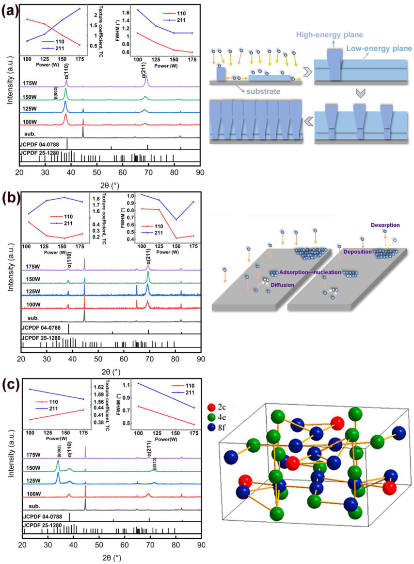
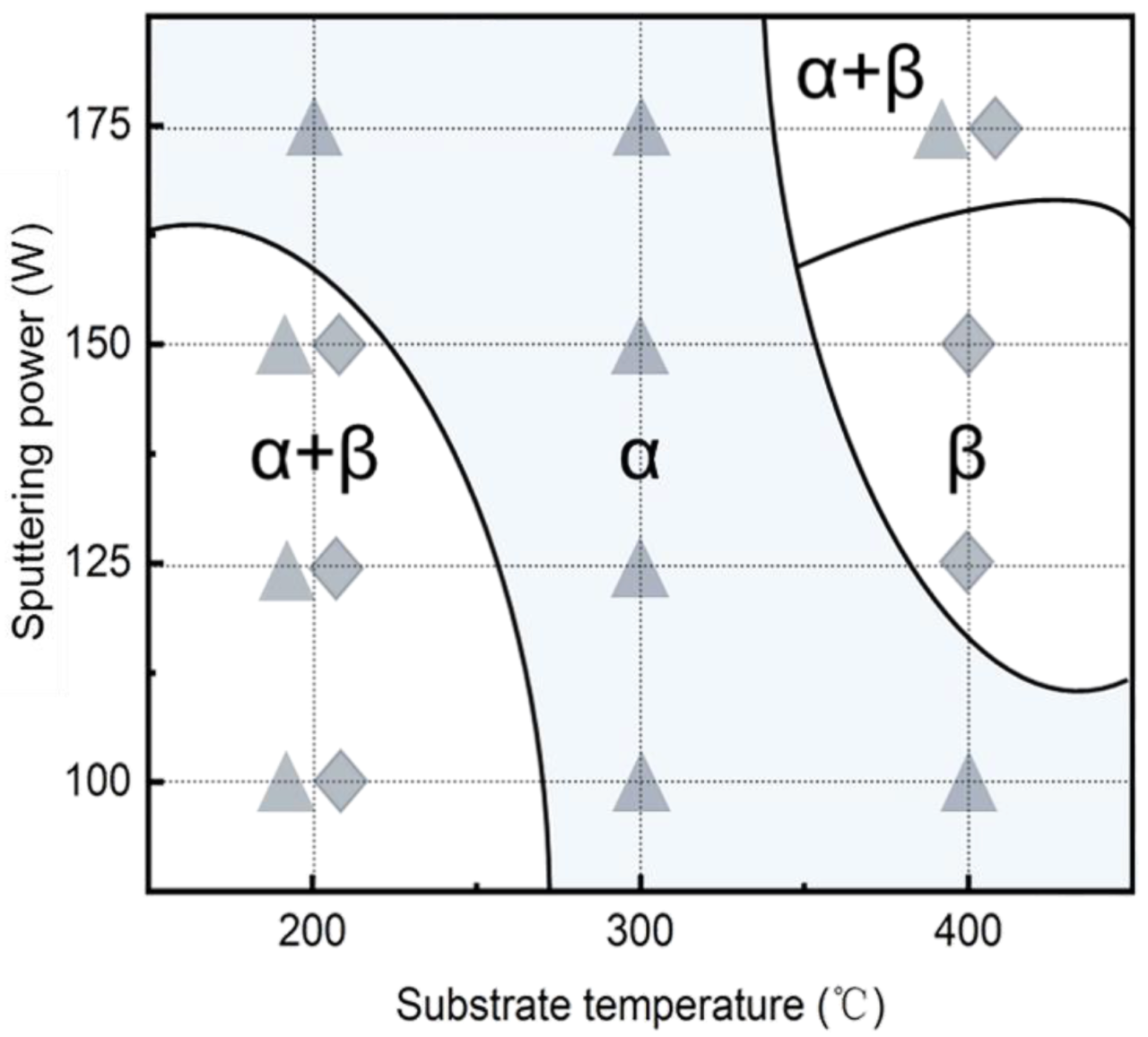
3.1. Crystalline Phase

Figure 2 shows XRD patterns of Ta coatings deposited on steel substrates at Tsub from 200 °C to 400 °C as a function of power, respectively. The relevant texture coefficient (TC) and full width at half maximum (FWHM) are illustrated in the inset.
At Tsub = 200 °C (Figure 2a), both α-Ta (JCPDF 04-0788) and β-Ta (JCPDF 25-1280) are detected in the coatings at Pspu =100 W, 125 W, and 150 W. When Pspu is further increased to 175 W, all diffraction peaks can be indexed to α-Ta, indicating that single-phased α-Ta coatings can be obtained by adjusting Pspu. To more accurately characterize the change of the orientation degree, we introduce the texture coefficient T C h k l , which can be evaluated using the following formula [17,18].
T C h k l = I h k l / I 0 h k l 1 / N I h k l / I 0 h k l
where, I h k l and I 0 h k l are the measured intensity of the h k l plane and standard intensity in the JCPDF card, respectively, and N is the number of reflections. The larger the T C h k l , the higher the orientation degree of the h k l plane. The fluctuation of T C 110 and T C 211 of α-Ta as a function of Pspu is shown in the top-left corner of Figure 2a. It is discovered that the T C 110 value decreases while the T C 211 value grows with increasing Pspu from 100 W to 175 W. As is shown in Figure 2a, the different crystallization processes of coatings with different thicknesses will affect the crystallization orientation. In the early growth stage, the plane with low surface energy occupies a large coverage area. When the island growth ends, the plane with high surface energy and a high longitudinal growth rate becomes higher and subsequently expands into the surrounding area, contributing to the compression of the plane with low surface energy. In the middle and late growth stages, the proportion of the plane with high surface energy eventually exceeds the plane with low surface energy. Meanwhile, as can be seen in the top-right corner of Figure 2a, the FWHM of (110) and (211) decrease with increasing power, indicating better crystallinity at the higher power [19]. In addition, the FWHM is related to both crystallite size and the stress of the crystallites. These effects can be separated using the Williamson–Hall method [20]. With the increase in sputtering power, the ionization rate of Ar will lead to the increase in deposition rate and more Ta atoms will accumulate near the nucleation point, resulting in an increase in the grain size of the Ta coating. As can be seen from Figure 2a, the diffraction peaks of coatings are getting closer to the standard peak lines with increasing power, meaning reduced stress. Therefore, the increased crystallite size and reduced stress together promote the decrease in FWHM.
At Tsub = 300 °C (Figure 2b), the diffraction peaks are all α-Ta at any powers. However, different degrees of wrinkling and peeling from substrates macroscopically were observed at the Pspu of 100 W, 125 W, and 175 W. The highest T C 211 and the lowest T C 110 were obtained at 150 W. Furthermore, the FWHM at 150 W is lower than that of other powers. As is shown in Figure 2b, at the relatively low power, there is not enough energy to diffuse particles reaching the substrate due to the low kinetic energy, leading to poor adhesion and incomplete crystallization. With the increase in the sputtering power, the crystallization of the coating becomes better. However, when the power is too high, the particles deposited on the substrate cannot diffuse enough and are covered by the newly incident particles because of the fast deposition rate, which is not conducive to the crystallization of the coating. Indeed, high nucleation energy may lead to excessive stress, cracks, and other defects inside the coating.
At Tsub = 400 °C (Figure 2c), α-Ta was detected as the pure phase at Pspu = 100 W. When the Pspu was elevated from 125 W to 175 W, the main diffraction peaks were indexed from β-Ta to the mixed phase of α-Ta and β-Ta. The β-Ta phase further grew with crystal planes oriented along (002), which is the densest plane [21], as is shown in Figure 2c. Myers et al. [15] showed that the phase of Ta coating was correlated with its thickness. This conclusion was based on the increase in the substrate temperature with the deposition time, resulting in higher atomic mobility on the coating surface. Gregory Abadias et al. [22] showed that the deposition process parameters did not affect the stability of the crystal phase of α-Ta or β-Ta, indicating that the initial nucleation stage and the energy barrier of the stable α-Ta or β-Ta nucleation were decisive for the phase.
Based on the experimental results in Figure 2, Figure 3 summarizes the evolution of the phase composition of Ta coatings prepared under different Tsub and Pspu conditions. It can be seen that α-Ta is formed under specific temperature and power conditions. During the deposition process of coatings, the effect of temperature and power on the coating structure can be attributed to the surface activity of the substrate and the energy of the Ta particles reaching the substrate. Accordingly, we speculate that the α-Ta formation may be attributed to the deposition energy which needs to be maintained within a certain range. On the grounds of this finding, we have reviewed some of the literature results. Hua Ren et al. [23] reported that the coatings deposited at intermediate bias voltages had pure α-Ta while they showed either mixed α-Ta with β-Ta or pure β-Ta at higher or lower bias voltages. Kazuhide Ino et al. [24] found that the coatings exhibited β-Ta if the bombarding energy was greater than 25 eV. It was confirmed that an appropriate energy input to the deposition of Ta atoms is required to synthesize α-Ta and excessive high energy may be unnecessary or even deleterious to α-Ta formation.
Therefore, Tsub and Pspu have a combined effect on growth and structural evolution of Ta coatings. They may interact with each other to keep a specific deposition energy. For the single-phased and homogeneous α-Ta coatings, the deposition conditions are 200 °C-175 W, 300 °C-150 W, and 400 °C-100 W.

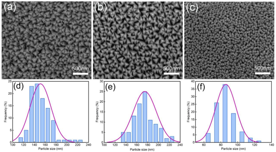
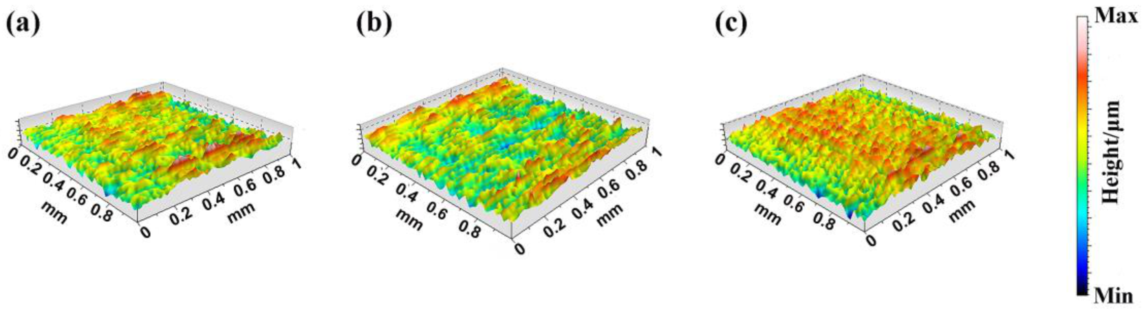
3.2. Surface Morphology

Figure 4 shows the surface morphology and grain distribution histogram of the Ta coatings deposited at Tsub-Pspu of 200 °C-175 W (Figure 4a,d), 300 °C-150 W (Figure 4b,e), and 400 °C-100 W (Figure 4c,f), respectively. The size distribution histograms were obtained by measuring more than 100 grains from the FESEM images.
As can be seen from the photographs, the surface morphology of single-phased α-Ta coatings deposited in these different conditions are all characterized by triangular pyramid-shaped particles with clear grain gaps, consistent with results published by M. Grosser et al. [25]. According to the Thornton structural zone model, the deposition pattern of Ta coating is the Z1 structure. This indicates that the diffusion distance of the particles is very small, and the initial nucleus tends to capture the orientation of the atoms on the coating surface at T/Tm < 0.1. While the substrate temperature increases from 200 °C–400 °C (0.1 < T/Tm < 0.3), the diffusion kinetic energy of surface adsorbed atoms increases, leading to increasing mobility of adsorbed atoms. The initially adsorbed atoms rapidly self-diffuse towards the equilibrium position, eventually trapped by larger grains to form the pyramid-shaped structure. The grain sizes of Ta coatings prepared at 200 °C-175 W and 300 °C-150 W range from 120 nm to 240 nm, while the grains of the sample prepared at 400 °C-100 W are smaller, within 60–120 nm, the surface of which is also denser than that in the other two conditions.
Figure 5 shows the 3D profiles of Ta coatings in different deposition conditions. Compared with the microstructural images obtained through SEM observation, the 3D profile contains a larger observation interval which is more suitable for observing the overall morphology distribution of millimeter-level samples. The surface height data of the Ta coating under different conditions were obtained according to the 3D profiles, as is listed in Table 3. Root mean square heights (Sq) of Ta coatings at 200 °C-175 W, 300 °C-150 W, and 400 °C-100 W were 0.0402 μm, 0.0184 μm, and 0.0132 μm, respectively. Arithmetic mean heights (Sa) of Ta coatings at 200 °C-175 W, 300 °C-150 W, and 400 °C-100 W were 0.0319 μm, 0.0145 μm, and 0.0103 μm, respectively. The results indicate that the surface of the Ta coating at 400 °C-100 W is flatter, while the roughness of the Ta coating at 200 °C-175 W is higher. According to the histogram results of the grain distribution in Figure 4, the coating grain size distributions at 400 °C-100 W and 300 °C-150 W have a concentrated grain size distribution, while the coatings at 200 °C-175 W are quite distributed between 130 nm and 170 nm, resulting in higher roughness.

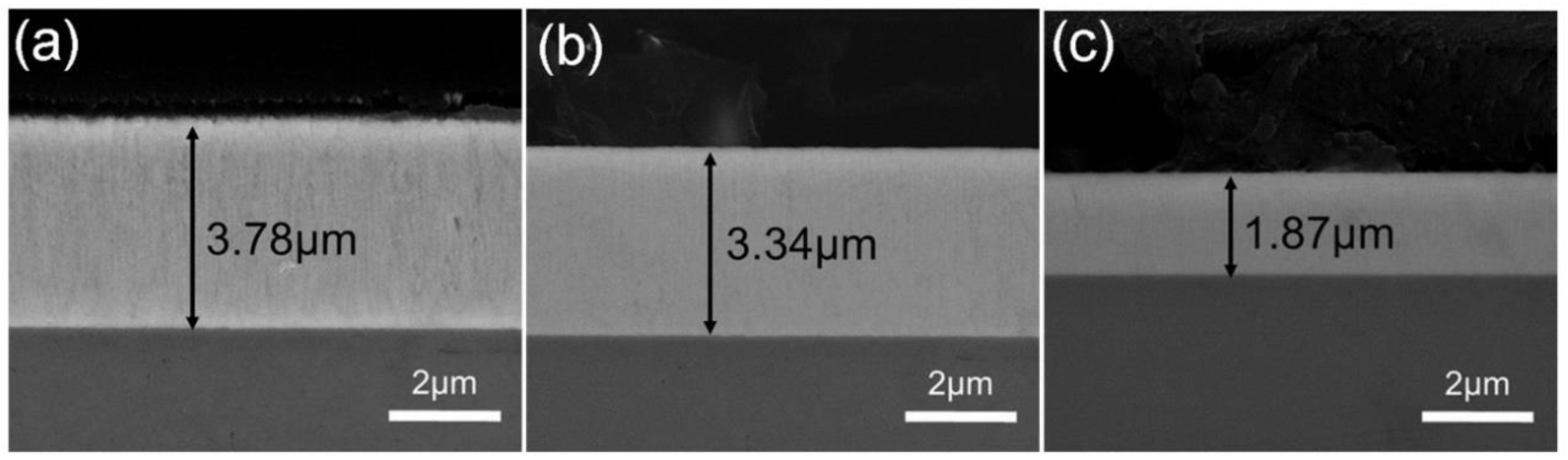
3.3. Cross-Sectional Morphology

Figure 6 shows the cross-sectional morphology of the Ta coatings deposited at Tsub-Pspu of 200 °C-175 W, 300 °C-150 W, and 400 °C-100 W.
The coatings exhibit a typical columnar crystal growth pattern mainly affected by the shadowing effect. The anisotropy of columnar crystal growth leads to a large competitive advantage for those crystals growing perpendicular to the interface, and columnar crystals in other directions are submerged as the coating thickens. In addition, the thicknesses of Ta coatings are approximately 3.78 μm, 3.34 μm, and 1.87 μm, respectively. When the sputtering power increases, the sputtered Ta atoms from the target increase, resulting in a high sputtering rate. However, according to the theory proposed by Kim et al. [26], a lower deposition rate enables atoms to move through the crystals across larger regions, and atoms are unlikely to be covered by subsequent adatom flux before being dampened in a particular location, potentially improving the mechanical properties of materials.

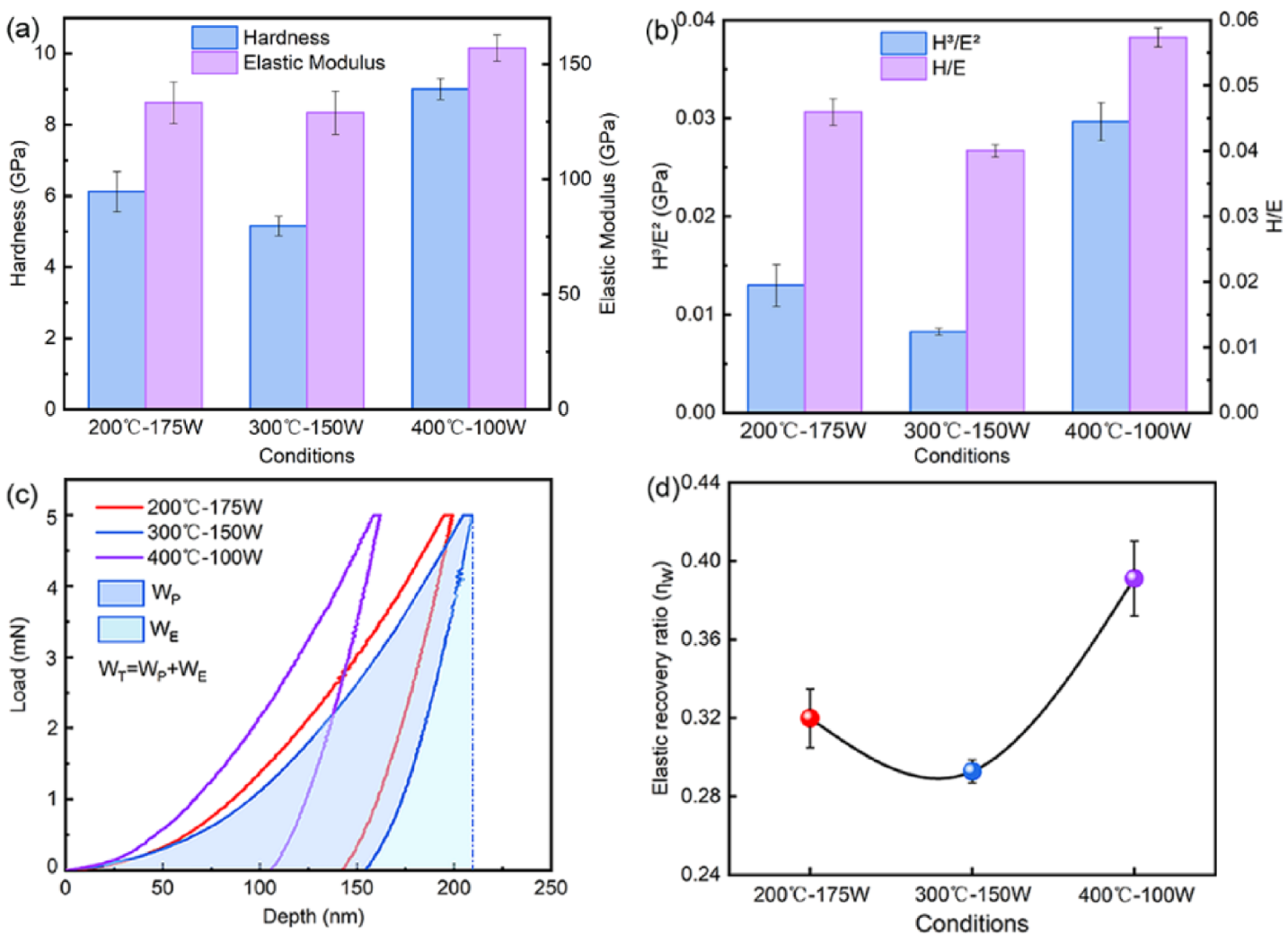
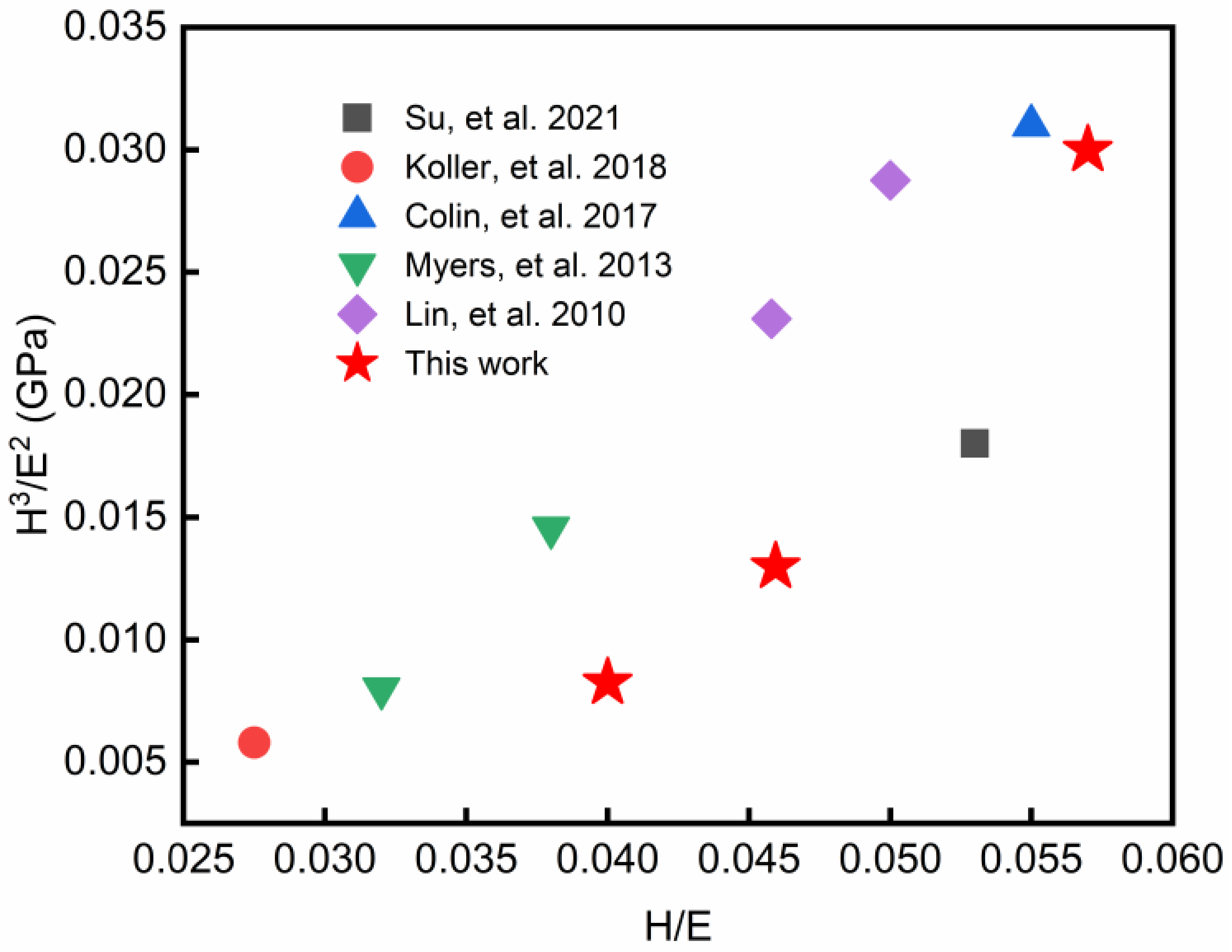
3.4. Hardness and Modulus
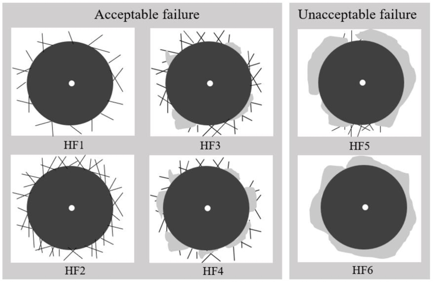
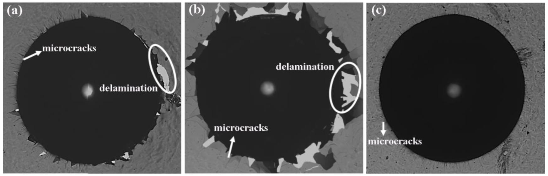
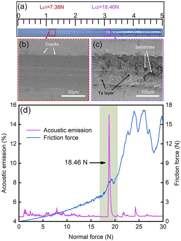
The corresponding hardness and elastic modulus were measured using an indentation tester for these coatings. It can be seen from Figure 7a that hardness and elastic modulus both reach the maximum value under the sputtering condition of 400 °C-100 W, 9 GPa, and 157 GPa, respectively. In general, the high hardness of coatings is usually attributed to their dense structure and small grain size. As shown in Figure 4, the Ta coating at 400 °C-100 W exhibits the densest structure with a minimal grain gap. On the other hand, this is concerned with the grain size that has an effect on mechanical properties of coatings due to the Hall–Petch (H-P) effect [27]. On the basis of the dislocation theory, grain boundaries are obstacles in the movement of dislocations, and refining grains can produce more grain boundaries. If the grain boundary structure does not change, a larger external force is required to generate dislocation plugging, thereby strengthening the material.
Furthermore, the enhanced hardness H is not a single important property of the hard coating. For many applications, H/E (elastic strain failure strength) [28] and H3/E2 (plastic deformation strength) [17] calculated by hardness and modulus are more important than their extremely high hardness. H/E and H3/E2 are important parameters of coating materials in the field of wear, which are positively related to the toughness of coatings and play a vital role in the crack resistance process [29]. Figure 7b shows the change in H/E and H3/E2 calculated from hardness (H) and elastic modulus (E). It can be seen that H/E and H3/E2 show similar variation trends, and both reach their highest at 400 °C-100 W, which are 0.057 and 0.030 GPa, respectively. It also demonstrates that the Ta coating at 400 °C-100 W has better crack resistance and toughness, with abilities to endure mechanical damage in abrasive wear applications and withstand impact energy from deformation to fracture [28].
The load–depth curves of Ta coatings at various sputtering conditions are illustrated in Figure 7c. The coatings were complied with an elastoplastic deformation according to the curves. In the nanoindentation test, some of the total energy (WT) was recovered as reversible elastic energy (WE), while some was lost as irreversible plastic deformation energy (WP). The elastic recovery ratio (ηw), which can be defined as ηw = WE/WT, is a measure to express the response of a material to indentation [30,31]. Take the coating prepared at 300 °C-150 W as an example; WE and WT are given by the areas under the loading and unloading curves, respectively, as shown in Figure 7c. The coating prepared at 400 °C-100 W has a higher ηw value of 0.39 in Figure 7d, indicating better resilience.
Figure 8 shows the comparison of the H/E and H3/E2 of α-Ta coatings prepared in this work with other literatures. In previous studies, the H/E and H3/E2 varied within a range of 0.0275–0.055 and 0.0058–0.031 GPa, respectively. Compared with other studies, the α-Ta coating at 400 °C-100 W in our work has higher H/E and comparable H3/E2 in contrast to G. Abadias et al. [21], which can be attributed to its high densification and homogeneous structure.

3.5. Adhesion

From actual applications of Ta coatings, the adhesion and integrity of the coating-substrate interface under projected loads are key performance concerns and the basis for improving coating performance and extended applications [11].
The adhesive performance was evaluated according to the reference standard. The standard diagram is shown in Figure 9, where grades one to four are acceptable failure and five to six are unacceptable failure. Figure 10 shows the results of the testing of α-Ta coatings under different conditions. The coatings prepared at 200 °C-175 W and 300 °C-150 W showed cracks and delamination, and the coating prepared at 300 °C-150 W peeled off from the substrate more seriously. Therefore, the coating ratings at 200 °C-175 W and 300 °C-150 W were HF3 and HF4, respectively. The coating prepared at 400 °C-100 W showed good adhesion without obvious delamination around the indentation. Compared with Figure 9, the overall coating rating was HF1. The better adhesion of the coating under 400 °C-100 W may be related to the dense structure and higher hardness.
According to the above analysis with respect to the morphology, hardness, and indentation test, it is determined that 400 °C-100 W is the optimal condition for forming Ta coatings. However, the coating indentation morphology can only qualitatively represent the adhesion of the coating to a certain extent. In this work, a scratch tester was used to quantify the adhesive properties of the Ta coating at 400 °C-100 W. The sudden variation of the acoustic emission and friction force is the deciding factor of every scratch mechanism.
The scratch morphologies of the Ta coating at 400 °C-100 W are shown in Figure 11a. As the applied load increases, the scratch width of the Ta coating surface also gradually increases, and the scratch area is clearly visible. In the scratch test, Lc1 is the corresponding load when cracks begin to appear and Lc2 is the minimum load for continuous peeling between the coating and the substrate, indicating the failure of the adhesion of the coating-substrate system. Usually, Lc2 is used to determine the failure of the coating [35]. From the enlarged image of Lc1 in Figure 11b, the appearance of small cracks can be seen, and the enlarged image of Lc2 in Figure 11c demonstrates that the coating begins to peel off from the substrate at this time, exposing the color of the substrate. According to the micro scratch curves in Figure 11d, it can be seen that Lc1 = 7.38 N and Lc2 = 18.46 N. The larger the Lc1, the stronger the cracking resistance of the coating. The longer the distance between Lc1 and Lc2, the better the coating’s resistance to crack propagation [36]. In previous work, Su et al. [32] found that mono-DC Ta coatings reached optimum adhesion compared with mono-PP and multi-PD coatings. The first fracture of mono-DC coating occurred when the load reached ~320 mN because the main diffraction peaks were β-Ta. Furthermore, Ay Ching Hee et al. [37], using DCMS technology, observed that the initiation of cracking in Ta coatings was at 2.5 N and the second critical load was at 18.6 N, with the coating separating from the substrate.
Compared with the studies in other literatures [32,37], the Ta coating prepared in this work has good adhesion as well as strong resistance to cracking.

4. Conclusions

In this study, Ta hard coatings were prepared on PCrNi1MoA steel substrates by direct current magnetron sputtering at various substrate temperatures (Tsub = 200–400 °C) and sputtering powers (Pspu = 100–175 W). The basic conclusions are as follows:
The growth and phase evolution were observed to be controlled by Tsub and Pspu simultaneously. Higher Pspu was required in order to obtain α-Ta coatings when the coatings are deposited at lower Tsub, and vice versa. Therefore, Tsub and Pspu interacted with each other and had a combined effect on coating growth. At a Tsub-Pspu at 200 °C-175 W, 300 °C-150 W, and 400 °C-100 W, single-phased and homogeneous α-Ta coatings were obtained.
The α-Ta coating deposited at Tsub-Pspu at 400 °C-100 W showed a relatively denser structure, finer grain (60–120 nm, and flatter surface, with the root mean square heights (Sq) of 0.0132 μm.
The α-Ta coating deposited at Tsub-Pspu at 400 °C-100 W exhibited a higher hardness (9 GPa), H/E (0.057), and H3/E2 (0.030 GPa), as well as an adhesion of 18.46 N.

Author Contributions

Conceptualization, C.L.; methodology, C.L.; software, C.L.; validation, C.L.; formal analysis, C.L.; investigation, C.L.; resources, J.P., Z.X. and Q.S.; data curation, C.L.; writing—original draft preparation, C.L.; writing—review and editing, J.P. and Z.X.; visualization, C.L.; supervision, C.W.; project administration, C.W. and Q.S.; funding acquisition, C.W. All authors have read and agreed to the published version of the manuscript.

Funding

This research was funded by Guangdong Major Project of Basic and Applied Basic Research (2021B0301030001), National Key R&D Program of China (2021YFB3802300), and Self-innovation Research Funding Project of Hanjiang Laboratory (HJL202012A001, HJL202012A002, HJL202012A003). And the APC was funded by Guangdong Major Project of Basic and Applied Basic Research (2021B0301030001).

Data Availability Statement

The data that support the findings of this study are all own results of the authors.

Conflicts of Interest

The authors declare no conflict of interest.

References

  1. Chen, X.; Yan, Q.; Ma, Q. Influence of the laser pre-quenched substrate on an electroplated chromium coating/steel substrate. Appl. Surf. Sci. 2017, 405, 273–279. [Google Scholar] [CrossRef]
  2. Sarraf, S.H.; Soltanieh, M.; Aghajani, A. Repairing the cracks network of hard chromium electroplated layers using plasma nitriding technique. Vacuum 2016, 127, 1–9. [Google Scholar] [CrossRef]
  3. Podgornik, B.; Massler, O.; Kafexhiu, F.; Sedlacek, M. Crack density and tribological performance of hard-chrome coatings. Tribol. Int. 2018, 121, 333–340. [Google Scholar] [CrossRef]
  4. Peng, X.; Xia, C.; Dai, X.; Wu, A.; Dong, L.; Li, D.; Tao, Y. Ablation behavior of NiCrAlY coating on titanium alloy muzzle brake. Surf. Coat. Technol. 2013, 232, 690–694. [Google Scholar] [CrossRef]
  5. Wang, D.; Lin, S.S.; Liu, L.Y.; Xue, Y.N.; Yang, H.Z.; Bai, J.L.; Zhou, K.S. Effect of Bias Voltage on Microstructure and Erosion Resistance of CrAlN Coatings Deposited by Arc Ion Plating. Rare Met. Mater. Eng. 2020, 49, 2583–2590. [Google Scholar]
  6. Matson, D.W.; McClanahan, E.D.; Lee, S.L.; Windover, D. Properties of thick sputtered Ta used for protective gun tube coatings. Surf. Coat. Technol. 2001, 146, 344–350. [Google Scholar] [CrossRef]
  7. Liu, L.L.; Xu, J.; Lu, X.; Munroe, P.; Xie, Z.H. Electrochemical Corrosion Behavior of Nanocrystalline beta-Ta Coating for Biomedical Applications. ACS Biomater Sci. Eng. 2016, 2, 579–594. [Google Scholar] [CrossRef]
  8. Niu, Y.; Chen, M.; Wang, J.; Yang, L.; Guo, C.; Zhu, S.; Wang, F. Preparation and thermal shock performance of thick α-Ta coatings by direct current magnetron sputtering (DCMS). Surf. Coat. Technol. 2017, 321, 19–25. [Google Scholar] [CrossRef]
  9. Traving, M.; Zienert, I.; Zschech, E.; Schindler, G.; Steinhögl, W.; Engelhardt, M. Phase analysis of TaN/Ta barrier layers in sub-micrometer trench structures for Cu interconnects. Appl. Surf. Sci. 2005, 252, 11–17. [Google Scholar] [CrossRef]
  10. Zhou, Y.M.; Xie, Z.; Xiao, H.N.; Hu, P.F.; He, J. Effects of deposition parameters on tantalum films deposited by direct current magnetron sputtering. J. Vac. Sci. Technol. A Vac. Surf. Film. 2009, 27, 109–113. [Google Scholar] [CrossRef]
  11. Gladczuk, L.; Patel, A.; Singh Paur, C.; Sosnowski, M. Tantalum films for protective coatings of steel. Thin Solid Film. 2004, 467, 150–157. [Google Scholar] [CrossRef]
  12. Al-masha’al, A.; Bunting, A.; Cheung, R. Evaluation of residual stress in sputtered tantalum thin-film. Appl. Surf. Sci. 2016, 371, 571–575. [Google Scholar] [CrossRef] [Green Version]
  13. Latif, R.; Jaafar, M.F.; Aziz, M.F.; Zain, A.R.M.; Yunas, J.; Majlis, B.Y. Influence of tantalum’s crystal phase growth on the microstructural, electrical and mechanical properties of sputter-deposited tantalum thin film layer. Int. J. Refract. Met. Hard Mater. 2020, 92, 105314. [Google Scholar] [CrossRef]
  14. Navid, A.A.; Hodge, A.M. Controllable residual stresses in sputtered nanostructured alpha-tantalum. Scr. Mater. 2010, 63, 867–870. [Google Scholar] [CrossRef]
  15. Myers, S.; Lin, J.; Souza, R.M.; Sproul, W.D.; Moore, J.J. The β to α phase transition of tantalum coatings deposited by modulated pulsed power magnetron sputtering. Surf. Coat. Technol. 2013, 214, 38–45. [Google Scholar] [CrossRef]
  16. Alami, J.; Eklund, P.; Andersson, J.; Lattemann, M.; Wallin, E.; Bohlmark, J.; Persson, P.; Helmersson, U. Phase tailoring of Ta thin films by highly ionized pulsed magnetron sputtering. Thin Solid Film. 2007, 515, 3434–3438. [Google Scholar] [CrossRef] [Green Version]
  17. Elmkhah, H.; Zhang, T.F.; Abdollah-zadeh, A.; Kim, K.H.; Mahboubi, F. Surface characteristics for the TiAlN coatings deposited by high power impulse magnetron sputtering technique at the different bias voltages. J. Alloys Compd. 2016, 688, 820–827. [Google Scholar] [CrossRef]
  18. Peng, B.; Xu, Y.X.; Du, J.W.; Chen, L.; Kim, K.H.; Wang, Q. Influence of preliminary metal-ion etching on the topography and mechanical behavior of TiAlN coatings on cemented carbides. Surf. Coat. Technol. 2022, 432, 128040. [Google Scholar] [CrossRef]
  19. Ferreira, F.; Sousa, C.; Cavaleiro, A.; Anders, A.; Oliveira, J. Phase tailoring of tantalum thin films deposited in deep oscillation magnetron sputtering mode. Surf. Coat. Technol. 2017, 314, 97–104. [Google Scholar] [CrossRef] [Green Version]
  20. Augustin, A.; Udupa, K.R.; Udaya, B.K. Crystallite size measurement and micro-strain analysis of electrodeposited copper thin film using Williamson-Hall method. AIP Conf. Proc. 2016, 1728, 020492. [Google Scholar]
  21. Colin, J.J.; Abadias, G.; Michel, A.; Jaouen, C. On the origin of the metastable β-Ta phase stabilization in tantalum sputtered thin films. Acta Mater. 2017, 126, 481–493. [Google Scholar] [CrossRef]
  22. Abadias, G.; Colin, J.J.; Tingaud, D.; Djemia; Belliard, L.; Tromas, C. Elastic properties of α- and β-tantalum thin films. Thin Solid Film. Vol. 2019, 688, 137403. [Google Scholar] [CrossRef]
  23. Ren, H.; Sosnowski, M. Tantalum thin films deposited by ion assisted magnetron sputtering. Thin Solid Film. 2008, 516, 1898–1905. [Google Scholar] [CrossRef]
  24. Ino, K.; Shinohara, T.; Ushiki, T.; Ohmi, T. Ion energy, ion flux, and ion species effects on crystallographic and electrical properties of sputter-deposited Ta thin films. J. Vac. Sci. Technol. A Vac. Surf. Film. 1997, 15, 2627–2635. [Google Scholar] [CrossRef]
  25. Grosser, M.; Schmid, U. The impact of sputter conditions on the microstructure and on the resistivity of tantalum thin films. Thin Solid Film. 2009, 517, 4493–4496. [Google Scholar] [CrossRef]
  26. Kim, J.H.; Holloway, P.H. Textured growth of cubic gallium nitride thin films on Si (100) substrates by sputter deposition. J. Vac. Sci. Technol. A Vac. Surf. Film. 2004, 22, 1591–1595. [Google Scholar] [CrossRef]
  27. Jimenez, M.J.M.; Antunes, V.; Cucatti, S.; Riul, A.; Zagonel, L.F.; Figueroa, C.A.; Wisnivesky, D.; Alvarez, F. Physical and micro-nano-structure properties of chromium nitride coating deposited by RF sputtering using dynamic glancing angle deposition. Surf. Coat. Technol. 2019, 372, 268–277. [Google Scholar] [CrossRef]
  28. Huang, B.; Liu, L.-T.; Du, H.-M.; Chen, Q.; Liang, D.-D.; Zhang, E.-G.; Zhou, Q. Effect of nitrogen flow rate on the microstructure, mechanical and tribological properties of CrAlTiN coatings prepared by arc ion plating. Vacuum 2022, 204, 111336. [Google Scholar] [CrossRef]
  29. Leyland, A.; Matthews, A. Design criteria for wear-resistant nanostructured and glassy-metal coatings. Surf. Coat. Technol. 2004, 177–178, 317–324. [Google Scholar] [CrossRef]
  30. Jha, K.K.; Suksawang, N.; Lahiri, D.; Agarwal, A. Evaluating initial unloading stiffness from elastic work-of-indentation measured in a nanoindentation experiment. J. Mater. Res. 2013, 28, 789–797. [Google Scholar] [CrossRef]
  31. Xia, Y.; Xu, Z.; Peng, J.; Shen, Q.; Wang, C. In-situ formation, structural transformation and mechanical properties Cr—N coatings prepared by MPCVD. Surf. Coat. Technol. 2022, 44, 128522. [Google Scholar] [CrossRef]
  32. Su, Y.; Huang, W.; Zhang, T.; Shi, C.; Hu, R.; Wang, Z.; Cai, L. Tribological properties and microstructure of monolayer and multilayer Ta coatings prepared by magnetron sputtering. Vacuum 2021, 189, 110250. [Google Scholar] [CrossRef]
  33. Koller, C.M.; Marihart, H.; Bolvardi, H.; Kolozsvári, S.; Mayrhofer, P.H. Structure, phase evolution, and mechanical properties of DC, pulsed DC, and high power impulse magnetron sputtered Ta–N films. Surf. Coat. Technol. 2018, 347, 304–312. [Google Scholar] [CrossRef]
  34. Lin, J.; Moore, J.J.; Sproul, W.D.; Lee, S.L.; Wang, J. Effect of Negative Substrate Bias on the Structure and Properties of Ta Coatings Deposited Using Modulated Pulse Power Magnetron Sputtering. IEEE Trans. Plasma Sci. 2010, 38, 3071–3078. [Google Scholar] [CrossRef]
  35. Shi, X.W.; Li, X.R.; Yao, N.; Wang, X.C.; Song, K.L.; Zhang, S. A Study on Magnetic Filter Controlling TiN Films Prepared by Arc Ion Plating. Appl. Mech. Mater. 2011, 117–119, 1071–1075. [Google Scholar] [CrossRef]
  36. Zhang, S.; Sun, D.; Fu, Y.; Du, H. Toughening of hard nanostructural thin films: A critical review. Surf. Coat. Technol. 2005, 198, 2–8. [Google Scholar] [CrossRef]
  37. Hee, A.C.; Jamali, S.S.; Bendavid, A.; Martin, P.J.; Kong, C.; Zhao, Y. Corrosion behaviour and adhesion properties of sputtered tantalum coating on Ti6Al4V substrate. Surf. Coat. Technol. 2016, 307, 666–675. [Google Scholar] [CrossRef]
Figure 1. Schematic diagram of magnetron sputtering.
Metals 13 00583 g001
Figure 2. XRD patterns of Ta coatings at different Tsub and Pspu. (a) 200 °C, (b) 300 °C, and (c) 400 °C.
Metals 13 00583 g002
Figure 3. Evolution of phase composition at different Tsub and Pspu, the α and β were indicated by Metals 13 00583 i001 and Metals 13 00583 i002, respectively.
Metals 13 00583 g003
Figure 4. FESEM images of surface morphology and grain size of the Ta coatings. (a,d) 200 °C-175 W, (b,e) 300 °C-150 W, and (c,f) 400 °C-100 W.
Metals 13 00583 g004
Figure 5. The 3D profile of the Ta coatings. (a) 200 °C-175 W, (b) 300 °C-150 W, and (c) 400 °C-100 W.
Metals 13 00583 g005
Figure 6. FESEM images of cross-sections of Ta coatings. (a) 200 °C-175 W, (b) 300 °C-150 W, and (c) 400 °C-100 W.
Metals 13 00583 g006
Figure 7. (a) H and E, (b) H/E and H3/E2, (c) load–depth curves, and (d) elastic recovery ratio of Ta coatings.
Metals 13 00583 g007
Figure 8. Comparison of the H/E and H3/E2 of α-Ta coatings with other literatures [15,21,32,33,34].
Metals 13 00583 g008
Figure 9. Reference standard for the evaluation of adhesion.
Metals 13 00583 g009
Figure 10. HRC indentation test of Ta coatings. (a) 200 °C-175 W, (b) 300 °C-150 W, and (c) 400 °C-100 W.
Metals 13 00583 g010
Figure 11. Scratch results of Ta coating prepared at 400 °C-100 W (a) OM of the scratch, (b,c) SEM morphology of the selected areas in Figure 4a, and (d) the micro scratch curve.
Metals 13 00583 g011
Table 1. Chemical composition of the alloy steel.
ElementCSiMnPSCr
wt.%0.3610.2520.4130.0110.0011.516
ElementNiVCuMoFe
wt.%1.5070.0920.0710.304Bal
Table 2. Deposition parameters for Ta coatings.
Deposition ConditionsParameters
Target99.95% Ta (Φ50 mm × H4 mm)
SubstratePCrNi1MoA steel (10 mm × 10 mm × 1 mm)
Distance between target and substrate70 mm
Ar pressure0.5 Pa
Deposition time1 h
Substrate temperature (Tsub)200–400 °C
Sputtering power (Pspu)100–175 W
Table 3. Height parameters of the Ta coatings in different conditions.
Height Parameters200 °C-175 W300 °C-150 W400 °C-100 WHeader
Unabbreviated Form
Sq/μm0.04020.01840.0132Root mean square height
Sp/μm0.1410.06770.0482Maximum peak height
Sv/μm0.1430.0710.0678Maximum pit height
Sz/μm0.2840.1390.116Maximum height
Sa/μm0.03190.01450.0103Arithmetic mean height
Disclaimer/Publisher’s Note: The statements, opinions and data contained in all publications are solely those of the individual author(s) and contributor(s) and not of MDPI and/or the editor(s). MDPI and/or the editor(s) disclaim responsibility for any injury to people or property resulting from any ideas, methods, instructions or products referred to in the content.

