
Evolution of the Shadow Effect with Film Thickness and Substrate Conductivity on a Hemispherical Workpiece during Magnetron Sputtering


Abstract
:Highlights
- There is a threshold thickness and incident angle below which the film is unaffected by the shadow effect during DC magnetron sputtering.
- The later-deposited film causes the earlier-deposited film to be affected by the shadow effect.
- The shadow effect manifests earlier for films deposited on the insulator SiO2 than for those deposited on the semiconductor Si.
- There is no need to worry about the shadow effect when the film deposited by oblique incident deposition has small thickness or the incident angle is small.
- The conductivity of the substrate could influence the shadow effect.
Abstract
1. Introduction
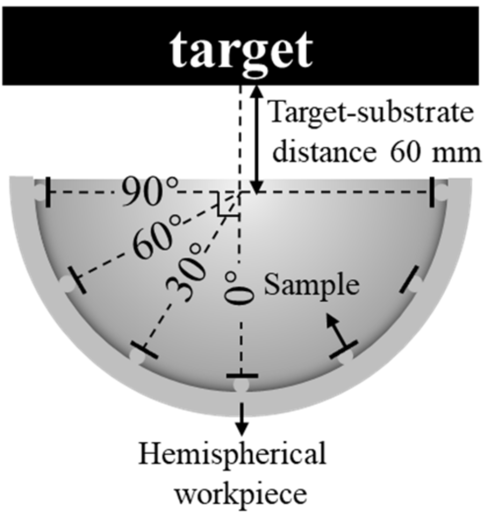
2. Materials and Methods
3. Results and Discussion
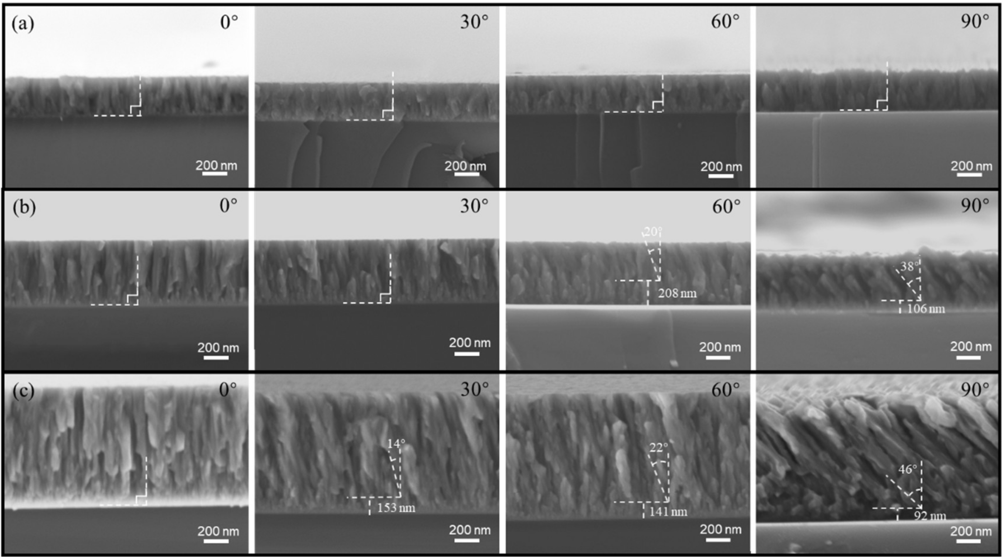
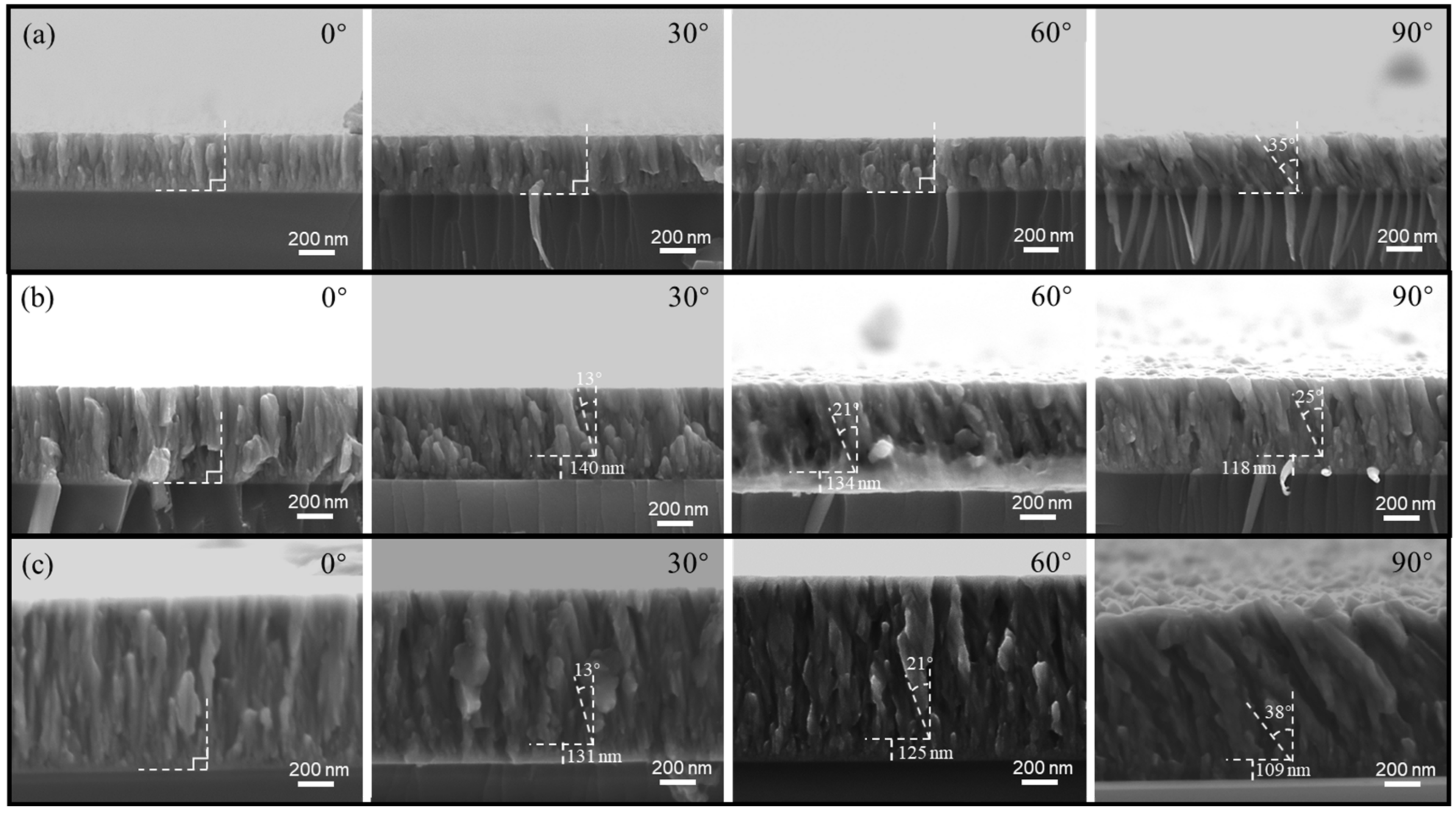
3.1. Cross-Sectional Morphology
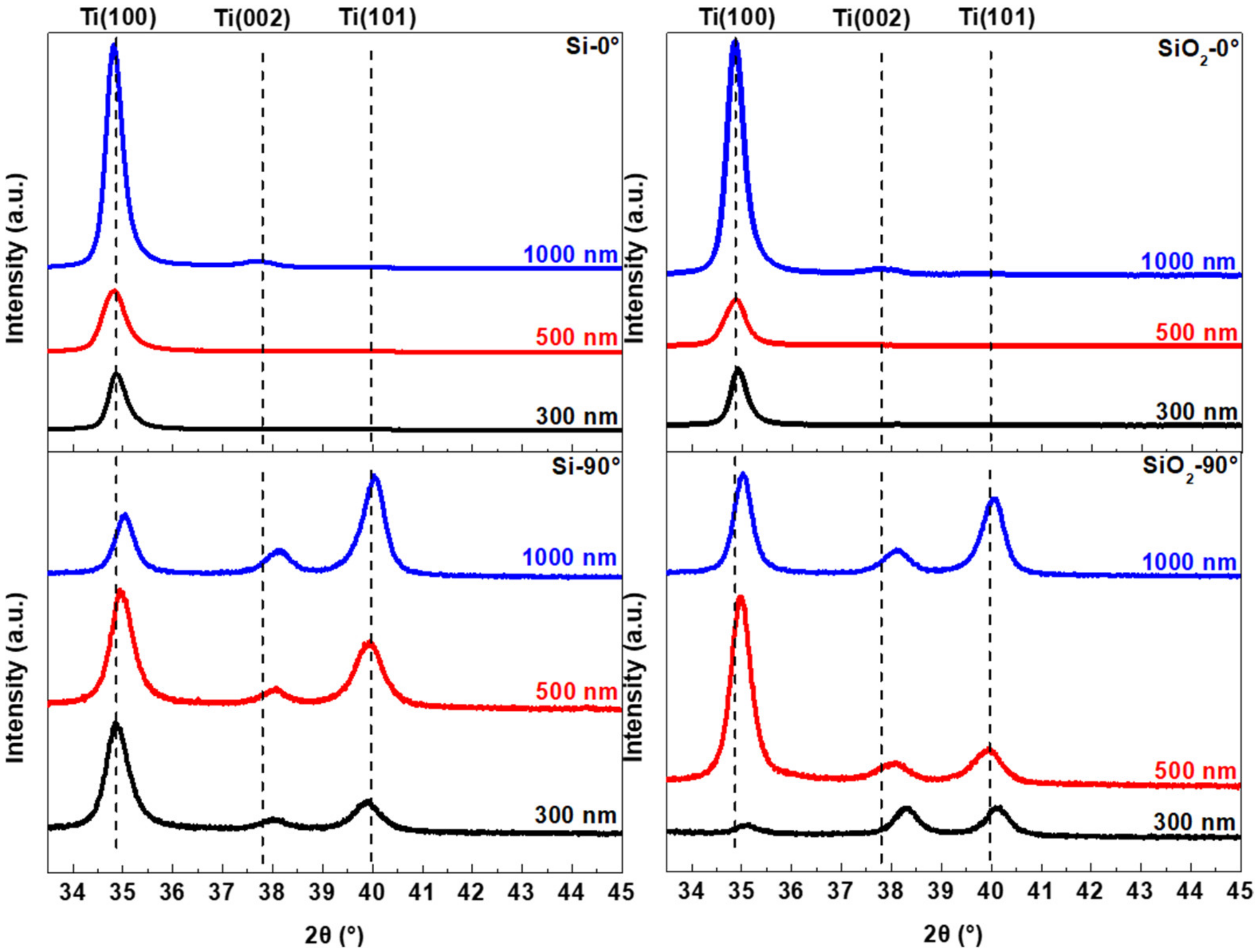
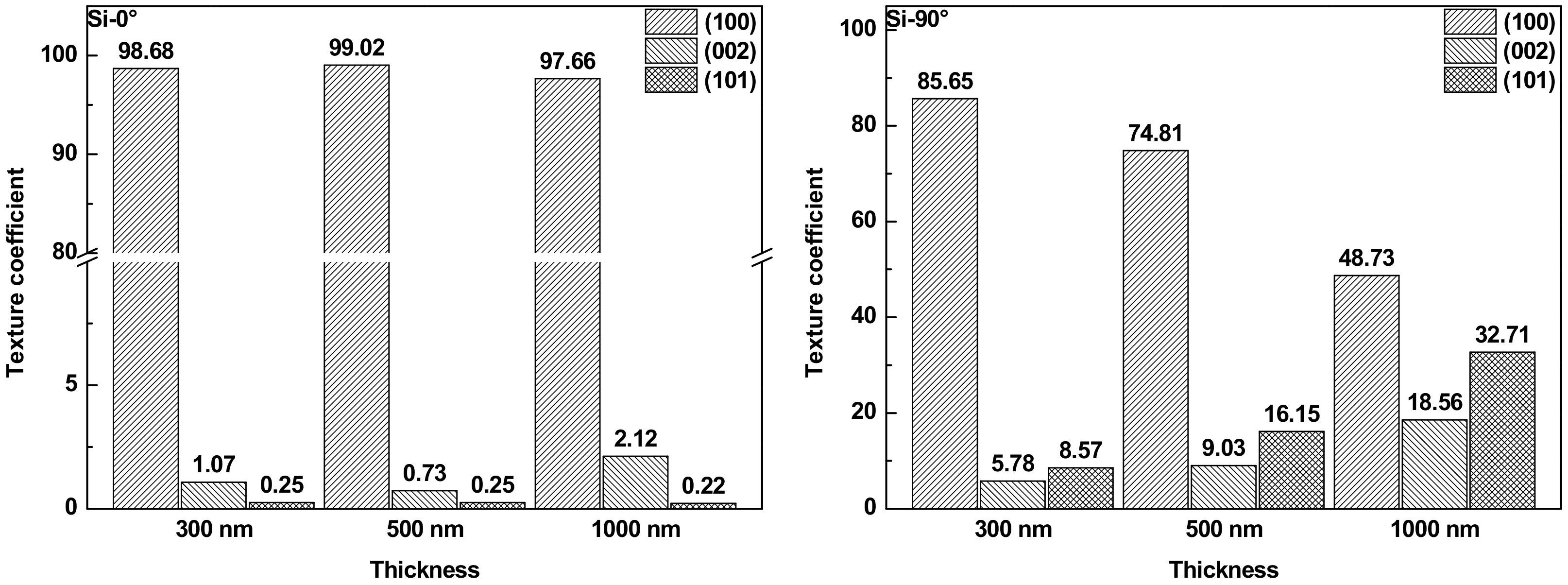
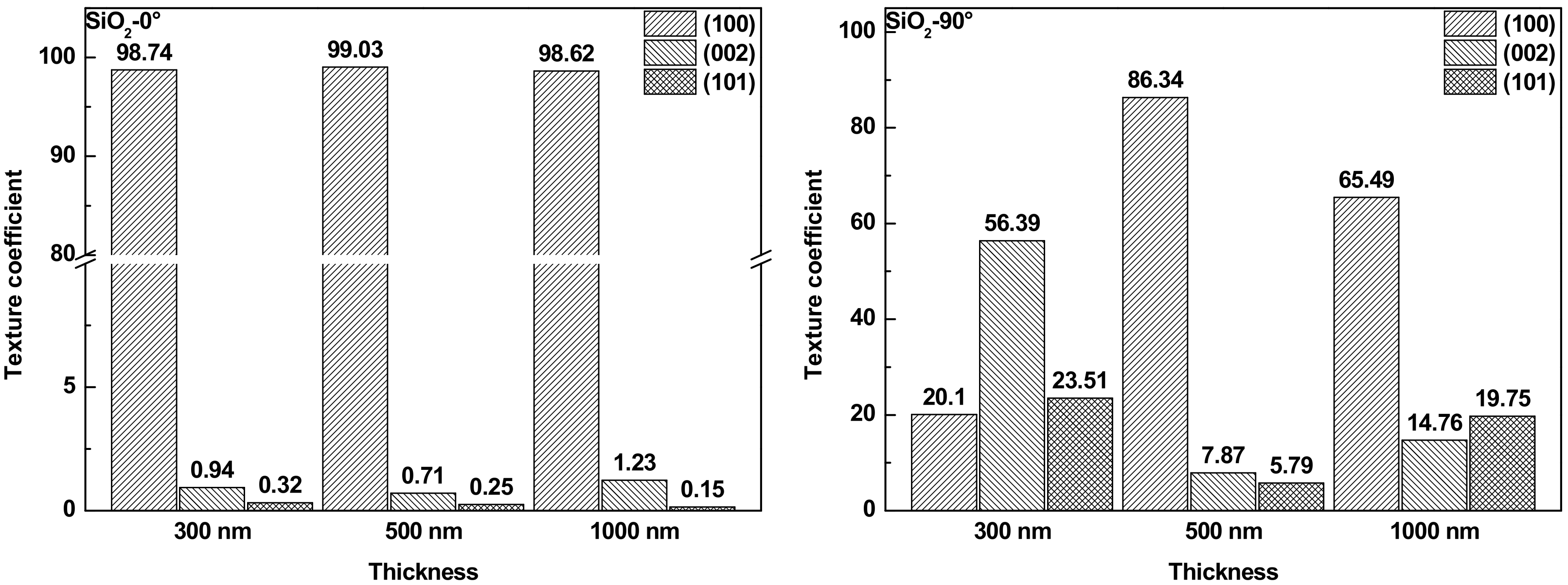
3.2. XRD
4. Conclusions
Author Contributions
Funding
Data Availability Statement
Conflicts of Interest
References
- Musil, J.; Vlček, J. A perspective of magnetron sputtering in surface engineering. Surf. Coat. Technol. 1999, 112, 162–169. [Google Scholar] [CrossRef]
- Kelly, P.; Arnell, R. Magnetron sputtering: A review of recent developments and applications. Vacuum 2000, 56, 159–172. [Google Scholar] [CrossRef]
- Verbeno, C.; Krohling, A.; Paschoa, A.; Bueno, T.; Soares, M.; Mori, T.; Larica, C.; Nascimento, V.; van Lierop, J.; Passamani, E.C. Cobalt nanowire arrays grown on vicinal sapphire templates by DC magnetron sputtering. J. Magn. Magn. Mater. 2020, 507, 166854. [Google Scholar] [CrossRef]
- Santos, R.; Chuvilin, A.; Modin, E.; Rodrigues, S.; Carvalho, S.; Vieira, M. Nanoporous thin films obtained by oblique angle deposition of aluminum on porous surfaces. Surf. Coat. Technol. 2018, 347, 350–357. [Google Scholar] [CrossRef]
- Phae-ngam, W.; Horprathum, M.; Chananonnawathorn, C.; Lertvanithphol, T.; Samransuksamer, B.; Songsiriritthigul, P.; Nakajima, H.; Chaiyakun, S. Oblique angle deposition of nanocolumnar TiZrN films via reactive magnetron co-sputtering technique: The influence of the Zr target powers. Curr. Appl. Phys. 2019, 19, 894–901. [Google Scholar] [CrossRef]
- Feng, C.; Zhang, W.; Wang, J.; Ma, H.; Liu, S.; Yi, K.; He, H.; Shao, J. Broadband antireflection film by glancing angle deposition. Opt. Mater. 2021, 111, 110720. [Google Scholar] [CrossRef]
- Haque, S.; Rao, K.; Misal, J.; Tokas, R.; Shinde, D.; Ramana, J.; Rai, S.; Sahoo, N. Study of hafnium oxide thin films deposited by RF magnetron sputtering under glancing angle deposition at varying target to substrate distance. Appl. Surf. Sci. 2015, 353, 459–468. [Google Scholar] [CrossRef]
- Bouaouina, B.; Mastail, C.; Besnard, A.; Mareus, R.; Nita, F.; Michel, A.; Abadias, G. Nanocolumnar TiN thin film growth by oblique angle sputter-deposition: Experiments vs. simulations. Mater. Des. 2018, 160, 338–349. [Google Scholar] [CrossRef]
- Liu, H.; Deng, Q.; Ma, D.; Li, Y.; Huang, N.; Leng, Y. The uniformity of TiN films deposited on the inner surfaces of a hemispherical workpiece by high-power pulsed magnetron sputtering. Int. J. Mod. Phys. B 2019, 33, 1950329. [Google Scholar] [CrossRef]
- Garcia-Martin, J.-M.; Alvarez, R.; Romero-Gomez, P.; Cebollada, A.; Palmero, A. Tilt angle control of nanocolumns grown by glancing angle sputtering at variable argon pressures. Appl. Phys. Lett. 2010, 97, 173103. [Google Scholar] [CrossRef] [Green Version]
- Hawkeye, M.; Brett, M. Glancing angle deposition: Fabrication, properties, and applications of micro- and nanostructured thin films. J. Vac. Sci. Technol. A Vac. Surf. Film. 2007, 25, 1317–1335. [Google Scholar] [CrossRef]
- Hao, J.; Jin, S.; Lu, G.-H.; Xu, H. Migration energy barriers and diffusion anisotropy of point defects on tungsten surfaces. Comput. Mater. Sci. 2020, 184, 109893. [Google Scholar] [CrossRef]
- Sbiaai, K.; Boughaleb, Y.; Mazroui, M.; Hajjaji, A.; Kara, A. Energy barriers for diffusion on heterogeneous stepped metal surfaces: Ag/Cu(110). Thin Solid Film. 2013, 548, 331–335. [Google Scholar] [CrossRef]
- Oliveira, J.; Ferreira, F.; Anders, A.; Cavaleiro, A. Reduced atomic shadowing in HiPIMS: Role of the thermalized metal ions. Appl. Surf. Sci. 2018, 433, 934–944. [Google Scholar] [CrossRef]
- Jiang, F.; Zhang, T.; Wu, B.; Yu, Y.; Wu, Y.; Zhu, S.; Jing, F.; Huang, N.; Leng, Y. Structure, mechanical and corrosion properties of TiN films deposited on stainless steel substrates with different inclination angles by DCMS and HPPMS. Surf. Coat. Technol. 2016, 292, 54–62. [Google Scholar] [CrossRef]
- Bobzin, K.; Bagcivan, N.; Immich, P.; Bolz, S.; Alami, J.; Cremer, R. Advantages of nanocomposite coatings deposited by high power pulse magnetron sputtering technology. J. Mater. Process. Technol. 2009, 209, 165–170. [Google Scholar] [CrossRef]
- Lai, M.-C.; Park, S.; Seol, Y. An energy stable finite difference method for anisotropic surface diffusion on closed curves. Appl. Math. Lett. 2022, 127, 107848. [Google Scholar] [CrossRef]
- Li, Y.; Bao, W. An energy-stable parametric finite element method for anisotropic surface diffusion. J. Comput. Phys. 2021, 446, 110658. [Google Scholar] [CrossRef]
- Shiraishi, T.; Katayama, K.; Yokouchi, T.; Shimizu, T.; Oikawa, T.; Sakata, O.; Uchida, H.; Imai, Y.; Kiguchi, T.; Konno, T.; et al. Effect of the film thickness on the crystal structure and ferroelectric properties of (Hf0.5Zr0.5)O2 thin films deposited on various substrates. Mater. Sci. Semicond. Process. 2017, 70, 239–245. [Google Scholar] [CrossRef]
- Feng, W.; Zhou, H.; Chen, F. Impact of thickness on crystal structure and optical properties for thermally evaporated PbSe thin films. Vacuum 2015, 114, 82–85. [Google Scholar] [CrossRef]
- Grigoriev, F.; Sulimov, V.; Tikhonravov, A. Atomistic simulation of the glancing angle deposition of SiO2 thin films. J. Non-Cryst. Solids 2019, 512, 98–102. [Google Scholar] [CrossRef]
- Chen, A.; Bu, Y.; Tang, Y.; Wang, Y.; Liu, F.; Xie, X.; Gu, J. Deposition-rate dependence of orientation growth and crystallization of Ti thin films prepared by magnetron sputtering. Thin Solid 2015, 574, 71–77. [Google Scholar] [CrossRef]
- Chawla, V.; Jayaganthan, R.; Chawla, A.; Chandra, R. Morphological study of magnetron sputtered Ti thin films on silicon substrate. Mater. Chem. Phys. 2008, 111, 414–418. [Google Scholar] [CrossRef]


| Sample | Si | ||
|---|---|---|---|
| 300 nm | 500 nm | 1000 nm | |
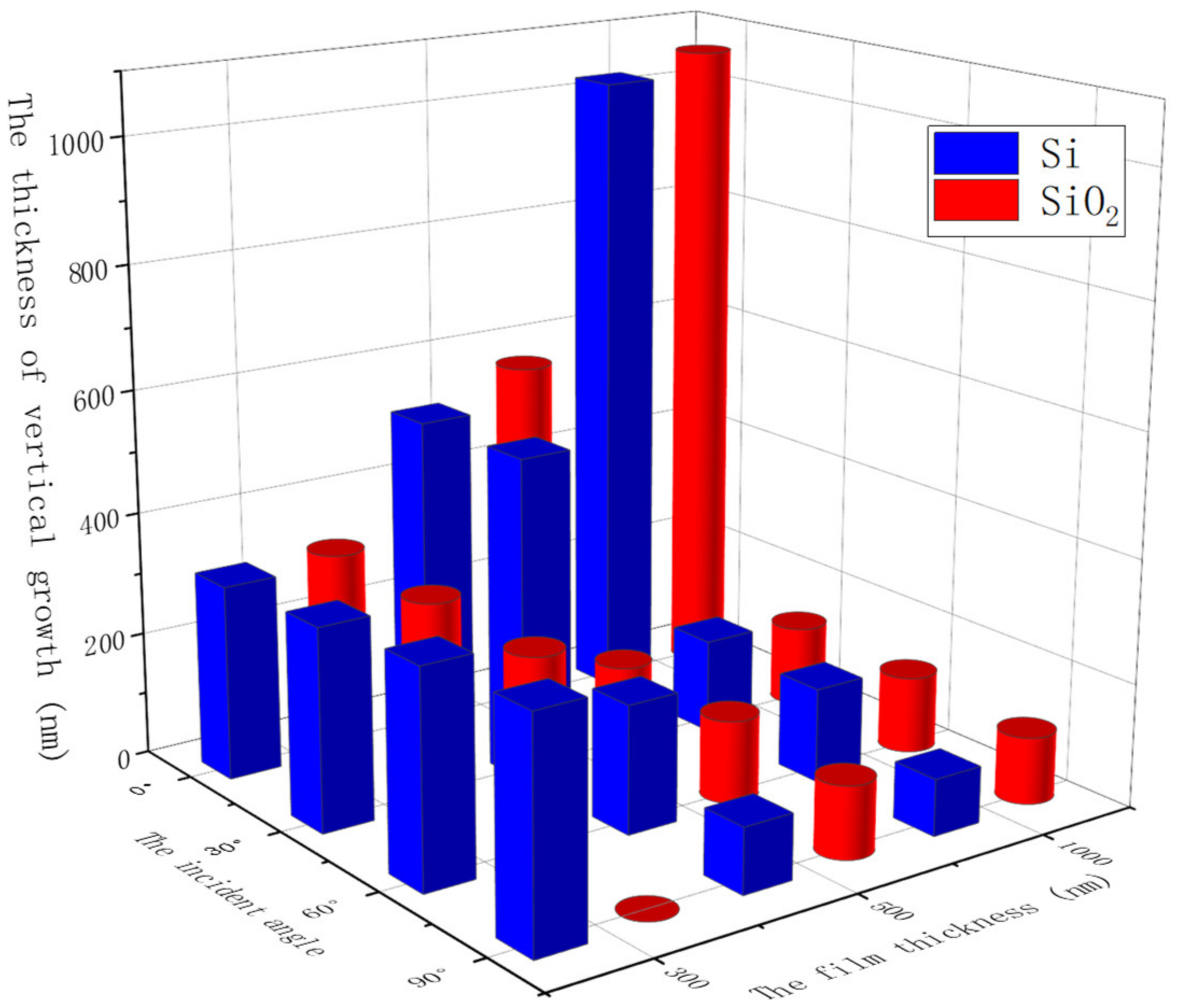
| Threshold of incident angle (°) | - | 60 | 30 |
| Sample | Film Total Thickness (nm) | Si | |||
|---|---|---|---|---|---|
| 0° | 30° | 60° | 90° | ||
| Threshold of film thickness (nm) | 300 | - | - | - | - |
| 500 | - | - | 208 | 106 | |
| 1000 | - | 153 | 153 | 92 | |
| Sample | SiO2 | ||
|---|---|---|---|
| 300 nm | 500 nm | 1000 nm | |
| Threshold of incident angle (°) | 90 | 30 | 30 |
| Sample | Film Thickness (nm) | SiO2 | |||
|---|---|---|---|---|---|
| 0° | 30° | 60° | 90° | ||
| Threshold of film thickness (nm) | 300 | - | - | - | 0 |
| 500 | - | 140 | 134 | 118 | |
| 1000 | - | 131 | 125 | 109 | |
Disclaimer/Publisher’s Note: The statements, opinions and data contained in all publications are solely those of the individual author(s) and contributor(s) and not of MDPI and/or the editor(s). MDPI and/or the editor(s) disclaim responsibility for any injury to people or property resulting from any ideas, methods, instructions or products referred to in the content. |
© 2023 by the authors. Licensee MDPI, Basel, Switzerland. This article is an open access article distributed under the terms and conditions of the Creative Commons Attribution (CC BY) license (https://creativecommons.org/licenses/by/4.0/).
Share and Cite
Liu, H.; Ma, D.; Li, Y.; You, L.; Leng, Y. Evolution of the Shadow Effect with Film Thickness and Substrate Conductivity on a Hemispherical Workpiece during Magnetron Sputtering. Metals 2023, 13, 165. https://doi.org/10.3390/met13010165
Liu H, Ma D, Li Y, You L, Leng Y. Evolution of the Shadow Effect with Film Thickness and Substrate Conductivity on a Hemispherical Workpiece during Magnetron Sputtering. Metals. 2023; 13(1):165. https://doi.org/10.3390/met13010165
Chicago/Turabian StyleLiu, Huaiyuan, Donglin Ma, Yantao Li, Lina You, and Yongxiang Leng. 2023. "Evolution of the Shadow Effect with Film Thickness and Substrate Conductivity on a Hemispherical Workpiece during Magnetron Sputtering" Metals 13, no. 1: 165. https://doi.org/10.3390/met13010165