Article

Laser Shock Peening of Ti6Al4V Alloy with Combined Nanosecond and Femtosecond Laser Pulses

1
Aviation Key Laboratory of Science and Technology on Advanced Surface Engineering, AVIC Manufacturing Technology Institute, Beijing 100024, China
2
State Key Laboratory of Tribology, Department of Mechanical Engineering, Tsinghua University, Beijing 100084, China
3
School of Mechanical Engineering and Automation, Beihang University, Beijing 100191, China
*
Author to whom correspondence should be addressed.
These authors contribute equal to this work.
Metals 2022, 12(1), 26; https://doi.org/10.3390/met12010026
Submission received: 19 November 2021 / Revised: 20 December 2021 / Accepted: 21 December 2021 / Published: 23 December 2021

Abstract

:
Laser shock peening (LSP) with nanosecond or femtosecond laser pulses is applied to improve the mechanical properties of metallic materials. Thus, it is necessary to compare the effects of different processing methods on microstructure changes and property improvement. In this study, nanosecond LSP (NLSP), femtosecond LSP (FLSP), and LSP with combined nanosecond and femtosecond laser pulses (F-NLSP) are conducted on Ti6Al4V alloys to compare the surface morphologies, in-depth microstructures, and nanohardness changes. In FLSP, the peened surface is smooth, and the affected depth is limited near the peened surface. NLSPed and F-NLSPed samples present rough surfaces due to the severe ablation process. Small equiaxed grains with no preferred grain orientation are denser in F-NLSPed samples than that in NLSPed samples. Compared with NLSPed samples, the affected depth and amplitude of in-depth nanohardness are larger in F-NLSPed samples. This is attributed to the increased laser absorption of incident laser on the treated surface by femtosecond laser pulses. The results in this study show the effects of different LSP methods and provide chances in engineering potentials for material property improvements.

1. Introduction

Surface treatment technologies have become promising methods in various industrial applications [1,2,3]. By increasing hardness, introducing compressive residual stress, and inducing microstructural refinement, laser shock peening ((LSP); the abbreviations in this study are summarized in Table 1) can improve the mechanical properties of metallic materials on the treated surface [1,4]. During LSP treatments, high-energy laser pulses irradiate on target materials or absorption layers to generate laser-induced plasma with high temperature and pressure in localized areas [5]. The expansion of laser-induced plasma generates shock waves into target materials under air conditions or with restriction of confinement layers. The severe plastic deformation with a high strain rate causes the generation of grain refinements and dislocations to improve the mechanical properties of target materials [2]. At the same time, compressive residual stress with an affected depth of 1–2 mm is induced after LSP processing. This retards the initiation and propagation of fatigue crack and surface corrosion [6].
Femtosecond laser and nanosecond laser pulses are usually applied with various strength mechanisms, processing methods, and application potentials [7,8,9]. According to the previous studies, different wavelengths affect the laser–matter and laser–plasma interaction, indicating that different wavelengths can affect the peening effects on material properties in LSP [10,11,12]. The potential influence of wavelength on the peening effects needs future studies considering the absorption properties of the target surface and the expansion of laser-induced plasma. Nanosecond laser shock peening (NLSP) has been already confirmed to improve the mechanical properties of metallic materials with or without absorption layers at the laser–matter interface [13,14]. NLSP with absorption layers is used as an efficient surface treatment to protect the thermal effect during nanosecond laser ablation [15]. During multiple laser spots processing, the shedding or ablation of the absorption layer is caused due to the overlapping of adjacent laser spots. This determines the limited applications due to the unstable surface topography and in-depth microstructural evolutions [15]. Thus, NLSP without absorption layers has been investigated in specific engineering applications with lower energies inputs and higher overlapping rates [16,17]. In this processing method, the metallic material is directedly irradiated by nanosecond laser pulses under confining conditions. The evaporation and the corresponding laser-induced plasma are caused by the ablation of target materials. With the confinement of the water layer or glass, a dominant shock wave is generated on the ablated surface with a pressure of several GPa. The low energy input with a single laser pulse results in the local surface ablation during NLSP [16,17,18].
Considering NLSP methods with or without absorption layers, the confinement layer (typical the deionized water or glass) is essential to suppress the expansion of laser-induced plasma and increase the plasma pressure during NLSP. When the confining water prevents the rapid expansion of the laser-induced plasma, the intensity of the shock wave is improved, and the pressure of plasma is increased with a high amplitude [19]. The application of confinement layers dominates the increase in sufficient shock wave pressure to deform the target materials plastically [20,21]. In contrast, femtosecond laser shock peening (FLSP) can be conducted directly under air conditions, which provides different engineering potentials [22,23,24]. In FLSP processing, milli-Joule-scale energy input (even micro-Joule-scale energy input [25,26]) is adopted, which is three orders of magnitude lower than that used in NLSP [20,22,23]. Due to the ultra-short duration characteristics, FLSP induces high shock wave pressure of several hundred GPa in the air with milli-Joule-scale energy [25,26], whereas 1–10 GPa pressure can be induced in NLSP with Joule-scale energy [13,14,20]. The introduction of water layers weakens the peening effects as strong ionization of confining medium shields the majority absorption of incident laser energy [20]. During FLSP, dense dislocation, refined grains, and compressive residual stresses are induced near the peened surface [27]. Thus, similar improvement of surface mechanical properties can be achieved with lower energy input, compared with NLSP, such as surface hardness [26,28], anti-corrosion properties [9,23], anti-fatigue properties [22,29]. Moreover, surface textures and ripples are formed on those peened surfaces to obtain the multifunctional surfaces, which is a unique characteristic of FLSP [25]. The adding effects of multi-cycles NLSP on the affected depths usually reach saturated values within 3–5 impacts [30]. LSP with combined nanosecond and femtosecond laser pulses (F-NLSP) offers a different way to increase the affected depth by the improvement of light absorption on target samples [24]. Totally, LSPs with femtosecond or nanosecond laser pulses are investigated under different conditions to clarify the material–laser interaction, microstructural evolution, and material property improvements. Thus, it is necessary to study the effects of different LSP methods on microstructure changes and mechanical property improvements.
In this study, NLSP, FLSP, and F-NLSP of Ti6Al4V alloys are conducted to study the effects on the changes of surface morphology, microstructure, and nanohardness. The surface morphologies and in-depth microstructural changes are characterized for un-treated and LSPed samples with different processing methods. Nanoindentation experiments were conducted to study the mechanical property changes before and after NLSP, FLSP, and F-NLSP experiments. This study aims to reveal the effects of different LSP methods on the surface morphology, microstructure and nanohardness of Ti6Al4V alloys.

2. Material and Methods

2.1. Material and LSP Experiments

The Ti6Al4V alloy was used in this study, with its chemical composition and mechanical properties listed in Table 2 and Table 3, respectively. Before LSP experiments, those as-received Ti6Al4V alloys were mechanically polished to remove the original surface defects. Ultrasonic cleanings with deionized water and alcohol were subsequently conducted for 10 min to avoid external contaminations.
Three different LSP methods were applied to study the microstructure changes, as shown in Figure 1. A femtosecond laser system with a pulse duration (tp) of 35 fs, wavelength (λ) of 800 nm, pulse frequency (f) of 1 kHz, and spot diameter (D) of 10 μm was used during FLSP processing. The FLSP experiments were conducted in the air to prevent the strong ionization of the confining medium. The laser scanning velocity (v), energy input (F), and overlapping length between adjacent scanning lines (Δx) were set as 8000 μm/s, 171.81 J/cm2, and 10 μm, respectively. Thus, according to Equations (1) and (2) [31], the overlapping rate between adjacent laser spots (η) and the overlapping rate between adjacent scanning lines (φ) are calculated as 21.46% and 29.52%, respectively.
η = 1 - v f × D 2
φ = 2 D 2 × arccos Δ x D 2 Δ x × D 2 Δ x 2 π D 2
In Equation (1), η is calculated with the relative size of the spot spacing (v/f) and D/2. In Equation (2), φ is the ratio of overlapping area and spot area, where the overlapping area is calculated by the geometrical relationship of adjacent scanning lines. During NLSP process, a Q-switched Nd-YAG laser (tp = 15 ns, λ = 1064 nm, F = 25 J, and D = 4 mm) was used. Both η and φ were equal to 50%. As shown in Figure 1a, the confining water layer of 2 mm was used to suppress the expansion of plasma and increase the pressure of laser-induced plasma. In the F-NLSP processing, FLSP under air conditions and NLSP under confining conditions were subsequently conducted in the same area. The detailed processing parameters in F-NLSP was with the same as the FLSP and NLSP processes. In the following results and discussions, samples treated by FLSP, NLSP, and F-NLSP were called FLSPed, NLSPed, and F-NLSPed samples, respectively.

2.2. Characterization Methods

The white light interferometer (WLI, NeXView, Middlefield, CT, USA) was used to characterize surface morphologies of the un-treated sample and LSPed samples treated by different processing methods. The scanning electron microscopy (SEM, Quanta 200FEG, Eindhoven, The Netherlands) was utilized to observe the microstructure changes of those original and laser-processed surfaces. Energy-dispersive X-ray spectroscopy (EDS, Quanta 200FEG, Eindhoven, the Netherlands) mappings were used to determine the elements’ distribution on the original and LSPed surfaces. During the EDS mappings, titanium, aluminum, vanadium, oxygen, and carbon were selected to analyze, and the detection areas are the same as the enlarged SEM observations to show the essential relation between morphology formation and element distribution.
The nanohardness experiments were conducted with a nano-indenter(NHT3, Buchs, Switzerland). Before the experiments, the un-treated, FLSPed, NLSPed, and F-NLSPed samples were first cut into 5 mm × 5 mm × 5 mm blocks. Those cubic blocks were cold-inlayed with resins, and the cross-sectional surfaces were mechanical polished. The first indention position, which was 10 μm below the LSPed or un-treated surfaces, was chosen, and the maximum detected distance was 1510 μm. Those experiments were conducted three times. The average values and the corresponding deviations were calculated. The loading, holding, and unloading times were set as 30 s, 5 s, and 30 s, respectively. The maximum loading force (Fn) was 5 mN.
Electron back-scattered diffraction (EBSD, Oxford Instruments, Abingdon, UK) experiments were conducted to study the in-depth changes of grain refinements and misorientations of un-treated and LSPed samples. Before EBSD studies, the 5 mm × 5 mm × 5 mm blocks were prepared and then split into half parts to investigate the cross-sections. The cross-sectional surfaces were polished, chemically etched, and cleaned with alcohol. In EBSD analysis, the direction of inverse pole figure (IPF) mapping was normal to the shock peening direction, as decoded in the IPF triangles. For un-treated and LSPed samples, the detected areas were 50 μm × 50 μm at a depth of 50 μm below the un-treated or LSPed surface, and the step size was set as 0.3 μm.

3. Results and Discussion

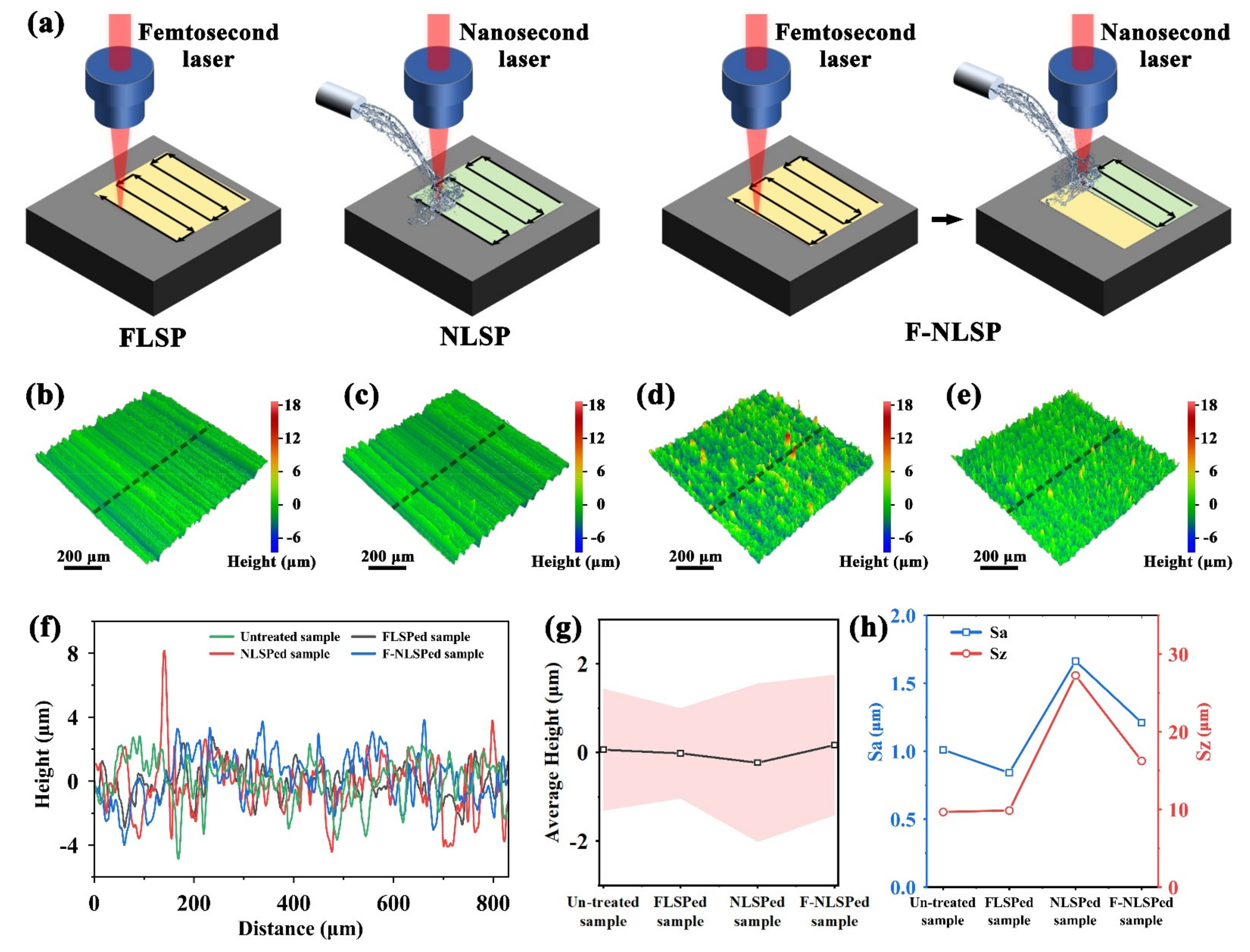
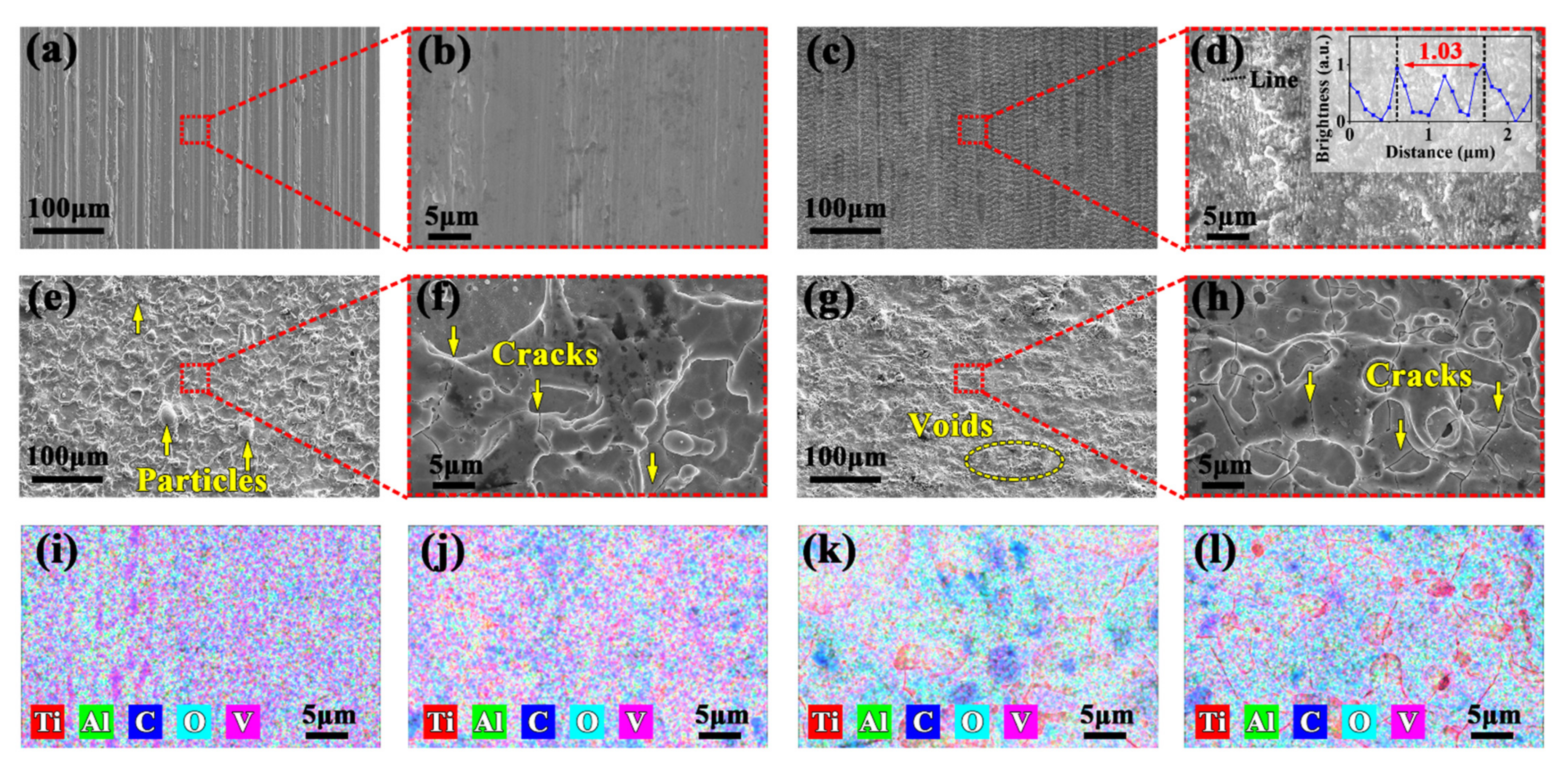
3.1. Surface Morphology Characterizations of Un-Treated and LSPed Samples

WLI images of surface morphologies of untreated, FLSPed, NLSPed, and F-NLSPed samples are shown in Figure 1b–e. The surface of the FLSPed sample presents slight changes compared to that of the un-treated sample, as shown in Figure 1b,c. This is attributed to the ultrafast interaction behaviors between femtosecond laser and target materials. Photon–electron interactions in the femtosecond scale dominate the entire FLSP process. Thus, the lattice motion is negligible within the femtosecond pulse duration and consequently results in a minimized heat-affected zone [22,32]. Micro-bulges and micro-valleys are observed on NLSPed and F-NLSPed surfaces, as shown in Figure 1d,e. The fluctuation of surface morphology on the NLSPed sample is obviously higher than that on the F-NLSPed samples, where those features are more uniform and denser in Figure 1e. The fabrication of those surface morphologies is due to the interaction process of nanosecond laser pulses and the different initial surfaces of un-treated and FLSPed surfaces during the subsequent NLSP processing, which will be further discussed based on the SEM and EDS observations in the next section.
To study the detailed surface morphologies of those surfaces, height changes are exported at the same positions from the 3D WLI images, as denoted in Figure 1b–e. The comparison plots are shown in Figure 1f with different colors. Altogether, FLSP, NLSP, and F-NLSP did not induce severe remelting recasts and surface reconstructions, as these plots are localized within ±2.5 μm, approximately. The red and blue height plots of NLSPed and F-NLSPed samples present several elevated positions, which are observed as the micro-bulges and micro-valleys in the corresponding 3D WLI images of Figure 1d,e. The average heights with the corresponding variances are shown in Figure 1g, where the slight ablation-induced height changes are determined. The comparison of Sa and Sz in Figure 1h clarified the surface roughness based on the whole surface analysis. FLSP induces an obvious decrease in height deviations, and those values are higher than that of the un-treated sample for NLSPed and F-NLSPed samples. That is reported as femtosecond-laser-induced surface flatting in some studies as the surface microstructures are removed and reconstructed due to the ultrafast laser ablation [33,34]. For NLSPed and F-NLSPed samples in Figure 1g,h, thermal expansion, thermal melting, potential mechanical damage, and vaporization ablation result in the increases in height variance, Sa and Sz, after nanosecond laser ablation [35]. Thus, FLSP causes slight changes on the peened surface compared to that of the un-treated sample, and the surfaces become rough for NLSPed and F-NLSPed samples.

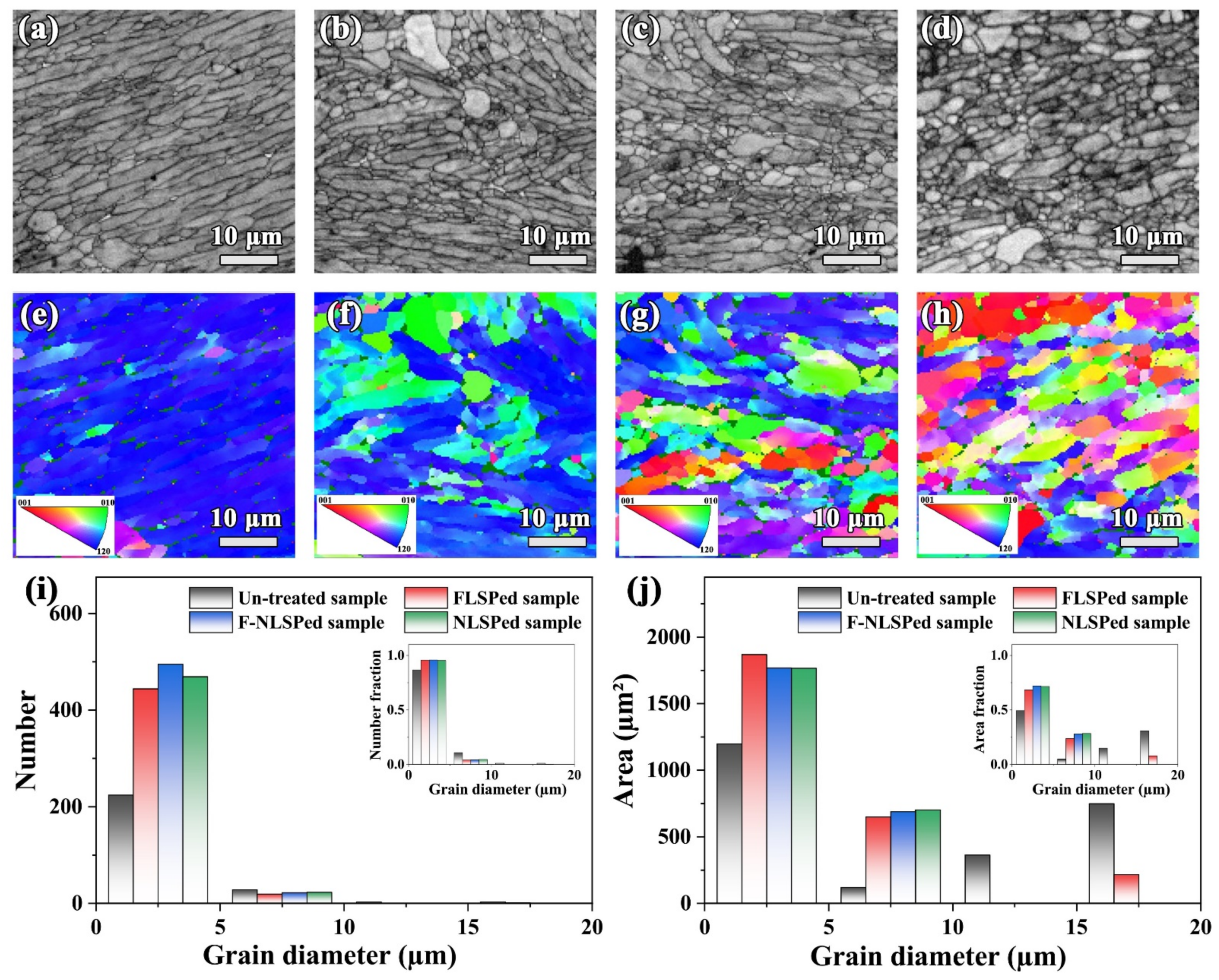
3.2. Surface Microstructural Changes of Un-Treated and LSPed Samples

In order to study the surface microstructural changes of un-treated and LSPed samples, SEM and EDS mapping analyses are conducted accordingly. Figure 2 shows the microstructural changes and elements distributions of un-treated, FLSPed, NLSPed, and F-NLSPed samples. The polishing scratches are observed on the un-treated surface in Figure 2a. Femtosecond laser pulses induce periodic microstructures like fish scales, as shown in Figure 2c. The enlarged view in Figure 2d presents discontinuous ripples and nonuniform nanoparticles, where the interval length between adjacent ripples is calculated as ~515 nm by Fourier transformation of the brightness normalization [36,37]. These micro-to-nano-structured surfaces are recognized as enhanced light absorption features, where light trapping can be introduced within the micro-to-nano structures, and the material absorption properties are increased [38,39]. As shown in Figure 2e, nanosecond laser ablation during NLSP processing induces many micro-scale particles. For F-NLSP processing, nanosecond laser ablation occurs on the pre-FLSPed surfaces, the re-solidification effects are limited, and many denser voids are formed, as presented in Figure 2g. In NLSP and F-NLSP, the effect of surface tension and Marangoni dominates the formation of rough surfaces [40]. During F-NLSP processing, significant recoil pressure effect and increased Marangoni force manifest that increased laser absorption property is modulated, and the laser–material coupling is enhanced [41,42,43]. Cracks are obviously shown in Figure 2f,h due to the combined effect of these three factors. At the same time, the increases in Marangoni forces and recoil pressure promote the enhancement of swirling and convection of melted materials, and denser cracks are observed for F-NLSPed samples [40,44].
EDS mapping was conducted to analyze the element distribution of un-treated, FLSPed, NLSPed, and F-NLSPed samples, respectively. The observation of surface microstructures and element distributions at the same areas reveals the surface oxidation behavior during different laser processing methods. On the surfaces of un-treated and FLSPed samples, as shown in Figure 2i,j, uniform element distributions are observed. This is owing to the ultrafast laser–materials interaction during the femtosecond laser process that encourages little oxidation on the surface. As presented in Figure 2k,l, oxygen is prominent on NLSPed and F-NLSPed samples, where Ti-O and V-O oxides are localized in the EDS mappings. V-C carbides start to form where cracks are prone to initiate [45]. The EDS mappings of Figure 2f,k, Figure 2h,l reveal that surface oxidation, cracks initiation, and microstructural morphology formation are all closely related. The change of laser processing methods is a fundamental key factor to define the surface morphology and microstructure changes. In all, femtosecond laser pulses induce periodic microstructures like fish scales with discontinuous ripples and nonuniform nanoparticles in FLSPed samples. Cracks formation are observed for NLSPed and F-NLSPed samples due to the severe ablation process.

3.3. In-Depth Microstructural Changes of Un-Treated and LSPed Samples

EBSD analyses of un-treated, FLSPed, NLSPed, and F-NLSPed samples were performed to observe the in-depth microstructural changes at a depth of 50 μm. The band contrast (BC) images, IPF mappings, and histogram comparisons of grain distribution are shown in Figure 3. As presented in Figure 3a, the un-treated sample consists of coarse lath grains. The lath grains are uniform-directed with a length scale of tens micrometers, and the misorientation angles of the lath grains are not distinguished, as shown in Figure 3e. For the FLSPed samples in Figure 3b, smaller refined equiaxed grains begin to generate near the peened surface, and the grains in the bottom parts remain in the lath shape. As depicted in Figure 3f, misorientation angles between adjacent grains and high-angle grain boundaries are fostered due to severe plastic deformation near the peened surface treated by FLSP. Rapid attenuation of the laser-induced shock wave in target materials localized the affected depth of grain features [22]. As shown in Figure 3c,g, dense, refined equiaxed grains are observed with an average size of several micrometers. The preferred grain orientation is further reduced after NLSP processing. For F-NLSPed samples, there are no preferred grain orientations in the IPF mappings, as presented in Figure 3d,h. In the whole detected area, the misorientation angles of refined equiaxed grains are totally distinguished with denser grains generated. At the same time, the uniform-directed lath grains vanish completely, as compared to the un-treated samples shown in Figure 3a. The small equiaxed grains in F-NLSPed samples are more uniform and denser than the NLSPed sample, which originate from the increased laser-coupling efficiency of samples pre-treated by femtosecond laser pulses during F-NLSP processing.
The number and area histograms of grains with different sizes are analyzed in Figure 3i,j. The insert histograms show the fraction changes of grain area and number, respectively. As shown in Figure 3i, the number of smaller grains (<5 μm) is 224 for un-treated samples, less than half of the numbers of LSPed samples. Specifically, this value peaks up at 495 for F-NLSPed samples. There are no grains larger than 10 μm are observed for those LSPed samples with different processing methods, and a few larger grains are still present for un-treated samples. In the insert histograms of the number fractions of grains with different sizes, the fraction of smaller grains (<5 μm) accounts for more than 95% for LSPed samples, and the grain diameter of 11% of the total grains is still larger than 5 μm for un-treated samples. The difference is significant when determining the areas of those grains, as presented in Figure 3j. The area of smaller grains (<5 μm) of un-treated samples is minimum, compared with that of the LSPed samples, and the fraction of smaller grains (<5 μm) is 49% smaller than that of larger grains (5–20 μm). Thus, considering the numbers and areas of grains with different sizes, the in-depth grain refinement is further clarified in FLSPed, NLSPed, and F-NLSPed samples. Owing to the limited penetration depth, smaller refined equiaxed grains are observed near the peened surface for FLSPed samples. Dense refined equiaxed grains are observed with an average size of several micrometers are generated for NLSPed and F-NLSPed samples in the entire detected areas due to severe plastic deformation. The increased laser-coupling efficiency determines the maximum fractions of grain area and number (<5 μm) in F-NLSPed samples.

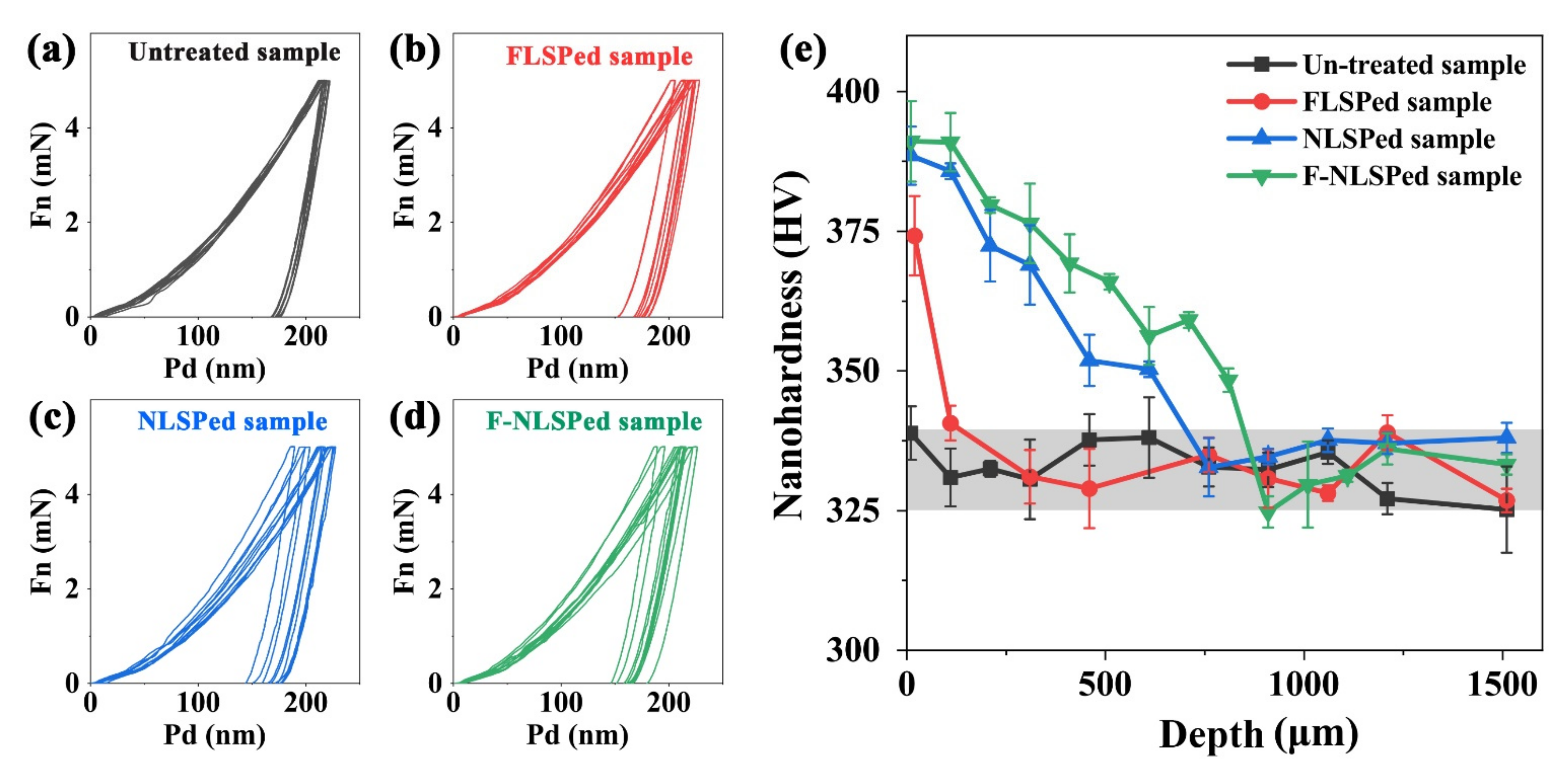
3.4. Nanoindentation Properties of Un-Treated and LSPed Surfaces

Nanoindentation experiments were conducted to analyze the mechanical property changes of un-treated and LSPed samples. Figure 4 presents the nanoindentation analyses of un-treated, FLSPed, NLSPed, and F-NLSPed samples. Fn and penetration depth (Pd) curve of un-treated, FLSPed, NLSPed, and F-NLSPed samples are shown in Figure 4a–d, respectively. As presented in Figure 4a, the values of Pd are near 175 nm for un-treated samples approximately. The values are stable and reveal the uniform distribution of nanohardness of un-treated samples. After FLSP processing, only one value of Pd decreases to 153 nm, as shown in Figure 4b. The other ones still stay within the localized range, similar to values of un-treated samples. The decrease in Pd values reveals that the surface is harder, and the nanohardness will be larger. In Figure 4c,d, nanoindentation experiments results show a wider range of Pd values for NLSPed and F-NLSPed samples, which means an increase in surface hardness of those samples. The increase in nanohardness is believed to be caused by the introduction of compressive stress and the generation of dislocations [46,47].
The in-depth values of nanohardness for the un-treated and LSPed samples are presented in Figure 4e. As shown in Figure 4e, the nanohardness near FLSPed, NLSPed, and F-NLSPed surfaces (at a depth of 10 μm) is maximum. With the increase in depth, the nanohardness decreases gradually. For FLSP processing, the hardened layer is restricted with several micrometers due to the ultrashort laser duration, and the penetration of laser-induced shock wave pressure vanishes rapidly [7,48,49]. For NLSPed and F-NLSPed surfaces, the maximum nanohardness is 388.5 and 391.6 HV, respectively. The increase in surface hardness is attributed to the combined effects of laser-induced thermal ablation and shock wave peening. During thermal ablation, the increased oxygen content in the remelted layer results in the surface hardening due to the oxygen diffusion in the liquid phase [50]. The oxygen distribution in Figure 2k,l also clarified the reconstruction of oxygen content. Nanosecond laser-induced shock wave pressure is also reported to increase the nanohardness for the introduction of compressive residual stress, grain refinement and dislocation [51,52,53]. A rapid decrease in nanohardness is observed for NLSPed and F-NLSPed surfaces with the increase in depth. The limitation depth of surface thermal ablation restricts the remelted hardening layer effect, as the heat-affected zone does not acquire significant additional oxygen. The attenuation of the laser shock wave along the depth direction contributes to the rapid decrease in nanohardness along the shock direction [51,54,55].
Compared with NLSPed, the affected depth and amplitude of in-depth nanohardness is larger for F-NLSPed samples. For the combined laser processing, higher nanohardness can be obtained during FLSP. At the same time, nano-to-micro-scale structures are fabricated on the peening surface [56,57]. During the second NLSP, the surface optical absorption is regulated due to the multiple reflectance-absorption behaviors [38,56]. The improvement of nanosecond laser absorption increases the light absorption into target materials. The increased light absorption promotes severe plastic deformation during NSLP. F-NLSPed samples present improved mechanical properties than that of NLSPed samples with one cycle condition. Multi-cycles NLSP is reported to increase the affected depth [30], and comparison studies between F-NLSP and multi-cycles NLSP need to be further conducted to clarify the applicability and feasibility of F-NLSP.

4. Conclusions

In this work, the changes of surface morphology, microstructure, and nanohardness of Ti6Al4V alloys are studied with different LSP methods. The surface morphologies and in-depth grain refinements are characterized for un-treated and LSPed samples. Nanoindentation experiments were conducted to study the mechanical property changes before and after LSP experiments. In FLSP, the peened surface is smooth, and the microstructure is affected near the peened surface. The surface roughness is similar for NLSPed and F-NLSPed samples. The morphologies of those surfaces present micro-bulges and micro-valleys in the corresponding 3D WLI images and SEM observations due to the ablation process. The observation of surface microstructures and element distributions at the same areas reveals the surface oxidation behavior in NLSP and F-NLSP. Dense refined equiaxed grains are observed with an average size of several micrometers for NLSPed and F-NLSPed samples in the whole detected areas due to severe plastic deformation. The fraction of smaller grains accounts for more than 95%, and the grain diameter of 11% of the total grains is still larger than 5 μm for un-treated samples in the EBSD analyses. The increased laser-coupling efficiency determines the maxi-mum fractions of grain area and number (<5 μm) in F-NLSPed samples. Compared with NLSPed, the affected depth and amplitude of in-depth nanohardness is larger for F-NLSPed samples. This is attributed to the improvement of laser absorption and severe plastic deformation. The results in this study show the effects of different LSP methods and provide chances in engineering potentials for material property improvements.

Author Contributions

Conceptualization, J.Y.; methodology, R.S., G.H. and J.Y.; software, G.H. and W.G.; validation, R.S. and J.Y.; formal analysis, G.H. and H.B.; investigation, R.S. and G.H.; resources, J.Y.; data curation, G.H. and J.Y.; writing—original draft preparation, G.H. and W.G.; writing—review and editing, R.S., G.H., H.B., J.Y. and W.G.; visualization, G.H. and H.B.; project administration, J.Y.; funding acquisition, J.Y. and R.S. All authors have read and agreed to the published version of the manuscript.

Funding

This research was supported by the National Natural Science Foundation of China (52101103, 52075289, 51775303).

Data Availability Statement

The data presented in this study are available in the article.

Conflicts of Interest

The authors declare no conflict of interest.

References

  1. Lei, Y.B.; Wang, Z.B.; Xu, J.L.; Lu, K. Simultaneous enhancement of stress- and strain-controlled fatigue properties in 316L stainless steel with gradient nanostructure. Acta Mater. 2019, 168, 133–142. [Google Scholar] [CrossRef]
  2. Lainé, S.J.; Knowles, K.M.; Doorbar, P.J.; Cutts, R.D.; Rugg, D. Microstructural characterisation of metallic shot peened and laser shock peened Ti–6Al–4V. Acta Mater. 2017, 123, 350–361. [Google Scholar] [CrossRef] [Green Version]
  3. Long, J.; Pan, Q.; Tao, N.; Dao, M.; Suresh, S.; Lu, L. Improved fatigue resistance of gradient nanograined Cu. Acta Mater. 2019, 166, 56–66. [Google Scholar] [CrossRef]
  4. Guo, W.; Wang, H.; Peng, P.; Song, B.; Zhang, H.; Shao, T.; Huan, H.; Qiao, H.; Qu, G.; Zhu, D.; et al. Effect of laser shock processing on oxidation resistance of laser additive manufactured Ti6Al4V titanium alloy. Corros. Sci. 2020, 170, 108655. [Google Scholar] [CrossRef]
  5. Guo, Y.; Wang, S.; Liu, W.; Sun, Z.; Zhu, G.; Xiao, T. Effect of laser shock peening on tribological properties of magnesium alloy ZK60. Tribol. Int. 2020, 144, 106138. [Google Scholar] [CrossRef]
  6. Lu, H.; Wang, Z.; Cai, J.; Xu, X.; Luo, K.; Wu, L.; Lu, J. Effects of laser shock peening on the hot corrosion behaviour of the selective laser melted Ti6Al4V titanium alloy. Corros. Sci. 2021, 188, 109558. [Google Scholar] [CrossRef]
  7. Zhang, C.; Dong, Y.; Ye, C. Recent Developments and Novel Applications of Laser Shock Peening: A Review. Adv. Eng. Mater. 2021, 23, 2001216. [Google Scholar] [CrossRef]
  8. Sano, Y.; Akita, K.; Sano, T. A mechanism for inducing compressive residual stresses on a surface by laser peening without coating. Metals 2020, 10, 816. [Google Scholar] [CrossRef]
  9. He, D.; Li, L.; Guo, W.; He, G.; Peng, P.; Shao, T.; Huan, H.; Zhang, G.; Han, G.; Yan, J. Improvement in oxidation resistance of Ti2AlNb alloys at high temperatures by laser shock peening. Corros. Sci. 2021, 184, 109364. [Google Scholar] [CrossRef]
  10. Margetic, V.; Pakulev, A.; Stockhaus, A.; Bolshov, M.; Niemax, K.; Hergenröder, R. Comparison of nanosecond and femtosecond laser-induced plasma spectroscopy of brass samples. Spectrochim. Acta Part B At. Spectrosc. 2000, 55, 1771–1785. [Google Scholar] [CrossRef]
  11. Harilal, S.S.; Kautz, E.J.; Jones, R.J.; Phillips, M.C. Spectro-temporal comparisons of optical emission, absorption, and laser-induced fluorescence for characterizing ns and fs laser-produced plasmas. Plasma Sources Sci. Technol. 2021, 30, 45007. [Google Scholar] [CrossRef]
  12. Förster, D.J.; Jäggi, B.; Michalowski, A.; Neuenschwander, B. Review on experimental and theoretical investigations of ultra-short pulsed laser ablation of metals with burst pulses. Materials 2021, 14, 3331. [Google Scholar] [CrossRef]
  13. Hatamleh, M.I.; Mahadevan, J.; Malik, A.; Qian, D.; Kovacevic, R. Prediction of Residual Stress Random Fields for Selective Laser Melted A357 Aluminum Alloy Subjected to Laser Shock Peening. J. Manuf. Sci. Eng. 2019, 141, 101011. [Google Scholar] [CrossRef]
  14. Bai, Y.; Wang, H.; Wang, S.; Huang, Y.; Chen, Y.; Zhang, W.; Ostendorf, A.; Zhou, X. Life cycle strengthening of high-strength steels by nanosecond laser shock. Appl. Surf. Sci. 2021, 569, 151118. [Google Scholar] [CrossRef]
  15. Yella, P.; Venkateswarlu, P.; Buddu, R.K.; Vidyasagar, D.V.; Sankara Rao, K.B.; Kiran, P.P.; Rajulapati, K.V. Laser shock peening studies on SS316LN plate with various sacrificial layers. Appl. Surf. Sci. 2018, 435, 271–280. [Google Scholar] [CrossRef]
  16. Zhu, Y.; Fu, J.; Zheng, C.; Ji, Z. Effect of laser shock peening without absorbent coating on the mechanical properties of Zr-based bulk metallic glass. Opt. Laser Technol. 2015, 75, 157–163. [Google Scholar] [CrossRef]
  17. Trdan, U.; Porro, J.A.; Ocaña, J.L.; Grum, J. Laser shock peening without absorbent coating (LSPwC) effect on 3D surface topography and mechanical properties of 6082-T651 Al alloy. Surf. Coat. Technol. 2012, 208, 109–116. [Google Scholar] [CrossRef] [Green Version]
  18. Yan, J.; Hodge, A.M. Study of β precipitation and layer structure formation in Al 5083: The role of dispersoids and grain boundaries. J. Alloys Compd. 2017, 703, 242–250. [Google Scholar] [CrossRef] [Green Version]
  19. Long, J.; Eliceiri, M.H.; Ouyang, Y.; Zhang, Y.; Xie, X.; Grigoropoulos, C.P. Effects of immersion depth on the dynamics of cavitation bubbles generated during ns laser ablation of submerged targets. Opt. Lasers Eng. 2021, 137, 106334. [Google Scholar] [CrossRef]
  20. Li, Y.; Ren, Z.; Jia, X.; Yang, W.; Nassreddin, N.; Dong, Y.; Ye, C.; Fortunato, A.; Zhao, X. The effects of the confining medium and protective layer during femtosecond laser shock peening. Manuf. Lett. 2021, 27, 26–30. [Google Scholar] [CrossRef]
  21. Nguyen, T.T.P.; Tanabe, R.; Ito, Y. Laser-induced shock process in under-liquid regime studied by time-resolved photoelasticity imaging technique. Appl. Phys. Lett. 2013, 102, 124103. [Google Scholar] [CrossRef]
  22. Kawashima, T.; Sano, T.; Hirose, A.; Tsutsumi, S.; Masaki, K.; Arakawa, K.; Hori, H. Femtosecond Laser Peening of Friction Stir Welded 7075-T73 Aluminum Alloys. J. Mater. Process. Technol. 2018, 262, 111–122. [Google Scholar] [CrossRef]
  23. Trdan, U.; Sano, T.; Klobčar, D.; Sano, Y.; Grum, J.; Šturm, R. Improvement of corrosion resistance of AA2024-T3 using femtosecond laser peening without protective and confining medium. Corros. Sci. 2018, 143, 46–55. [Google Scholar] [CrossRef]
  24. He, G.; Yan, J.; Zhu, D.; Xie, J. Improvement of laser shock peening depth through regulation of surface optical absorption. Adv. Mater. Interfaces 2021, 8, 2101232. [Google Scholar] [CrossRef]
  25. Wang, H.; Pöhl, F.; Yan, K.; Decker, P.; Gurevich, E.L.; Ostendorf, A. Effects of femtosecond laser shock peening in distilled water on the surface characterizations of NiTi shape memory alloy. Appl. Surf. Sci. 2019, 471, 869–877. [Google Scholar] [CrossRef]
  26. Lu, C.; Ge, L.; Zhu, B.; Li, Y.; Chen, X.; Zeng, X.; Chen, Y. Effective femtosecond laser shock peening on a Mg–3Gd alloy at low pulse energy 430 µJ of 1 kHz. J. Magnes. Alloys 2019, 7, 529–535. [Google Scholar] [CrossRef]
  27. Zhu, D.Z.; Yan, J.F.; Liang, Z.W.; Xie, J.W.; Bai, H.L. Laser stripping of Ag shell from Au@Ag nanoparticles. Rare Met. 2021, 40, 3454–3459. [Google Scholar] [CrossRef]
  28. Nakano, H.; Tsuyama, M.; Miyauti, S.; Shibayanagi, T.; Tsukamoto, M.; Abe, N. Femtosecond and nanosecond laser peening of stainless steel. J. Laser Micro Nanoeng. 2010, 5, 175–178. [Google Scholar] [CrossRef]
  29. Sano, T.; Eimura, T.; Hirose, A.; Kawahito, Y.; Katayama, S.; Arakawa, K.; Masaki, K.; Shiro, A.; Shobu, T.; Sano, Y. Improving Fatigue Performance of Laser-Welded. Metals 2019, 9, 1192. [Google Scholar] [CrossRef] [Green Version]
  30. Lu, J.Z.; Wu, L.J.; Sun, G.F.; Luo, K.Y.; Zhang, Y.K.; Cai, J.; Cui, C.Y.; Luo, X.M. Microstructural response and grain refinement mechanism of commercially pure titanium subjected to multiple laser shock peening impacts. Acta Mater. 2017, 127, 252–266. [Google Scholar] [CrossRef]
  31. Ma, J.; He, G.; Jia, Z.; Wang, X.; Wang, J. Solution of maximum laser ablation depth based on dynamic energy distribution model. Mater. Manuf. Process. 2019, 34, 1719–1725. [Google Scholar] [CrossRef]
  32. Chichkov, B.N.; Momma, C.; Nolte, S.; von Alvensleben, F.; Tünnermann, A. Femtosecond, picosecond and nanosecond laser ablation of solids. Appl. Phys. A Mater. Sci. Process. 1996, 63, 109–115. [Google Scholar] [CrossRef]
  33. Li, T.; Guo, Y.; Mizutani, M.; Xu, S. Surface smoothing of bulk metallic glasses by femtosecond laser double-pulse irradiation. Surf. Coat. Technol. 2021, 408, 126803. [Google Scholar] [CrossRef]
  34. Fan, Z.; Sun, X.; Zhuo, X.; Mei, X.; Cui, J.; Duan, W.; Wang, W.; Zhang, X.; Yang, L. Femtosecond laser polishing yttria-stabilized zirconia coatings for improving molten salts corrosion resistance. Corros. Sci. 2021, 184, 109367. [Google Scholar] [CrossRef]
  35. Gao, J.; Cao, Y.; Lu, L.; Hu, Z.; Wang, K.; Guo, F.; Yan, Y. Study on the interaction between nanosecond laser and 6061 aluminum alloy considering temperature dependence. J. Alloys Compd. 2021, 892, 162044. [Google Scholar] [CrossRef]
  36. Lin, Q.; Fan, Z.J.; Wang, W.; Yan, Z.; Zheng, Q.; Mei, X. The effect of spot overlap ratio on femtosecond laser planarization processing of SiC ceramics. Opt. Laser Technol. 2020, 129, 106270. [Google Scholar] [CrossRef]
  37. Chen, L.; Richter, B.; Zhang, X.; Ren, X.; Pfefferkorn, F.E. Modification of surface characteristics and electrochemical corrosion behavior of laser powder bed fused stainless-steel 316L after laser polishing. Addit. Manuf. 2020, 32, 101013. [Google Scholar] [CrossRef]
  38. Wang, Q.; Samanta, A.; Toor, F.; Shaw, S.; Ding, H. Colorizing Ti-6Al-4V surface via high-throughput laser surface nanostructuring. J. Manuf. Process. 2019, 43, 70–75. [Google Scholar] [CrossRef]
  39. Ackerl, N.; Gugger, P.; Wegener, K. Laser marking and coloration of Ti-6Al-4V with ultrashort pulses. J. Laser Appl. 2020, 32, 32013. [Google Scholar] [CrossRef]
  40. Temmler, A.; Pirch, N. Investigation on the mechanism of surface structure formation during laser remelting with modulated laser power on tool steel H11. Appl. Surf. Sci. 2020, 526, 146393. [Google Scholar] [CrossRef]
  41. Zou, M.; Zhang, Y.; Cai, Z.; Li, C.; Sun, Z.; Yu, C.; Dong, Z.; Wu, L.; Song, Y. 3D Printing a Biomimetic Bridge-Arch Solar Evaporator for Eliminating Salt Accumulation with Desalination and Agricultural Applications. Adv. Mater. 2021, 33, 2102443. [Google Scholar] [CrossRef] [PubMed]
  42. Liu, H.; Lin, W.; Lin, Z.; Ji, L.; Hong, M. Self-Organized Periodic Microholes Array Formation on Aluminum Surface via Femtosecond Laser Ablation Induced Incubation Effect. Adv. Funct. Mater. 2019, 29, 1903576. [Google Scholar] [CrossRef]
  43. Yan, J.; Zhu, D.; Xie, J.; Shao, Y.; Xiao, W. Light Tailoring of Internal Atomic Structure of Gold Nanorods. Small 2020, 16, 2001101. [Google Scholar] [CrossRef] [PubMed]
  44. Yao, L.; Huang, S.; Ramamurty, U.; Xiao, Z. On the formation of “Fish-scale” morphology with curved grain interfacial microstructures during selective laser melting of dissimilar alloys. Acta Mater. 2021, 220, 117331. [Google Scholar] [CrossRef]
  45. Petronić, S.; Čolić, K.; Đorđević, B.; Milovanović, D.; Burzić, M.; Vučetić, F. Effect of laser shock peening with and without protective coating on the microstructure and mechanical properties of Ti-alloy. Opt. Lasers Eng. 2020, 129. [Google Scholar] [CrossRef]
  46. Dai, F.Z.; Geng, J.; Tan, W.S.; Ren, X.D.; Lu, J.Z.; Huang, S. Friction and wear on laser textured Ti6Al4V surface subjected to laser shock peening with contacting foil. Opt. Laser Technol. 2018, 103, 142–150. [Google Scholar] [CrossRef]
  47. Lu, J.; Lu, H.; Xu, X.; Yao, J.; Cai, J.; Luo, K. High-performance integrated additive manufacturing with laser shock peening –induced microstructural evolution and improvement in mechanical properties of Ti6Al4V alloy components. Int. J. Mach. Tools Manuf. 2020, 148, 103475. [Google Scholar] [CrossRef]
  48. Ageev, E.I.; Bychenkov, V.Y.; Ionin, A.A.; Kudryashov, S.I.; Petrov, A.A.; Samokhvalov, A.A.; Veiko, V.P. Double-pulse femtosecond laser peening of aluminum alloy AA5038: Effect of inter-pulse delay on transient optical plume emission and final surface micro-hardness. Appl. Phys. Lett. 2016, 109, 211902. [Google Scholar] [CrossRef]
  49. Hoppius, J.S.; Kukreja, L.M.; Knyazeva, M.; Pöhl, F.; Walther, F.; Ostendorf, A.; Gurevich, E.L. On femtosecond laser shock peening of stainless steel AISI 316. Appl. Surf. Sci. 2018, 435, 1120–1124. [Google Scholar] [CrossRef] [Green Version]
  50. Kümmel, D.; Linsler, D.; Schneider, R.; Schneider, J. Surface engineering of a titanium alloy for tribological applications by nanosecond-pulsed laser. Tribol. Int. 2020, 150, 106376. [Google Scholar] [CrossRef]
  51. Yin, M.; Cai, Z.; Li, Z.; Zhou, Z.; Wang, W.; He, W. Improving impact wear resistance of Ti-6Al-4V alloy treated by laser shock peening. Trans. Nonferrous Met. Soc. China 2019, 29, 1439–1448. [Google Scholar] [CrossRef]
  52. Švábenská, E.; Pizurová, N.; Roupcová, P.; Chlupová, A.; Brajer, J.; Foldyna, J.; Schneeweiss, O. Effect of shock wave on microstructure of silicon steel. Surf. Interfaces 2020, 20, 100415. [Google Scholar] [CrossRef]
  53. Wu, J.; Che, Z.; Zou, S.; Cao, Z.; Sun, R. Surface Integrity of TA19 Notched Simulated Blades with Laser Shock Peening and Its Effect on Fatigue Strength. J. Mater. Eng. Perform. 2020, 29, 5184–5194. [Google Scholar] [CrossRef]
  54. Zhang, H.; Cai, Z.; Wan, Z.; Peng, P.; Zhang, H.; Sun, R.; Che, Z.; Guo, C.; Li, B.; Guo, W. Microstructure and mechanical properties of laser shock peened 38CrSi steel. Mater. Sci. Eng. A 2020, 788. [Google Scholar] [CrossRef]
  55. Rodopoulos, C.A.; Romero, J.S.; Curtis, S.A.; De los Rios, E.R.; Peyre, P. Effect of controlled shot peening and laser shock peening on the fatigue performance of 2024-T351 aluminum alloy. J. Mater. Eng. Perform. 2003, 12, 414–419. [Google Scholar] [CrossRef]
  56. Garcell, E.M.; Singh, S.C.; Li, H.; Wang, B.; Jalil, S.A.; Guo, C. Comparative study of femtosecond laser-induced structural colorization in water and air. Nanoscale Adv. 2020, 2, 2958–2967. [Google Scholar] [CrossRef]
  57. Cheng, C.W. Ablation of copper by a scanning Gaussian beam of a femtosecond laser pulse. Int. J. Adv. Manuf. Technol. 2017, 92, 151–156. [Google Scholar] [CrossRef]
Figure 1. Surface morphology characterizations of un-treated and LSPed surfaces. (a) Schematics of FLSP, NLSP, and F-NLSP, respectively; Surface morphologies of (b) untreated, (c) FLSPed, (d) NLSPed, and (e) F-NLSPed samples, respectively; (f) Heights changes along different detecting lines in (be); (g) Changes of average height with the corresponding variances; (h) Surface roughness.
Metals 12 00026 g001
Figure 2. Surface microstructural changes of un-treated and LSPed surfaces. Surface microstructures of (a) un-treated, (c) FLSPed, (e) NLSPed, and (g) F-NLSPed samples, (b,d,f,h) show the corresponding enlarged view in the selected areas; Surface elements mappings of (i) un-treated, (j) FLSPed, (k) NLSPed, and (l) F-NLSPed samples.
Metals 12 00026 g002
Figure 3. EBSD analyses for in-depth microstructural changes of un-treated and LSPed samples. BC images of in-depth microstructures of (a) un-treated, (b) FLSPed, (c) NLSPed, and (d) F-NLSPed samples; IPF mappings of (e) un-treated, (f) FLSPed, (g) NLSPed, and (h) F-NLSPed samples; Histogram comparisons of (i) the number and (j) the area of grains for un-treated and LSPed samples.
Metals 12 00026 g003
Figure 4. Nanoindentation analyses of un-treated and LSPed surfaces. The Fn–Pd curve of (a) un-treated, (b) FLSPed, (c) NLSPed, and (d) F-NLSPed samples; (e) Nanohardness of un-treated and LSPed surfaces.
Metals 12 00026 g004
Table 1. List of abbreviations used in this study.
AbbreviationFull Form
LSPLaser shock peening
NLSPNanosecond laser shock peening
FLSPFemtosecond laser shock peening
F-NLSPLSP with combined nanosecond and femtosecond laser pulses
LSPedTreated after NLSP, FLSP, or F-NLSP
NLSPedTreated by NLSP
FLSPedTreated by FLSP
F-NLSPedTreated by F-NLSP
SEMScanning electron microscope
WLIWhite light interferometer
EDSEnergy-dispersive X-ray spectroscopy
FnLoading force
PdPenetration depth
EBSDElectron back-scattered diffraction
IPFInverse pole figure
BCBand contrast
Table 2. Chemical composition of Ti6Al4V alloy employed in this study (wt.%).
AlVFeCNHOTi
6.144.160.040.0050.010.0070.14Bal.
Table 3. Mechanical properties of Ti6Al4V alloy employed in this study.
Density
(kg/m3)
Young Modulus
(GPa)
Yield Stress
(MPa)
Ultimate Stress
(MPa)
Elongation
(%)
450011088795516
Publisher’s Note: MDPI stays neutral with regard to jurisdictional claims in published maps and institutional affiliations.

