
Investigating Nanoindentation Creep Behavior of Pulsed-TIG Welded Inconel 718 and Commercially Pure Titanium Using a Vanadium Interlayer


Abstract
:1. Introduction
2. Materials and Methods
2.1. Microstructural Caharacterization
2.2. Nanoindentation
2.3. Calculation Methods
2.3.1. Hardness and Elastic Modulus
2.3.2. Indentation Strain Rate
2.3.3. Indentation Stress
2.3.4. Creep Stress Exponent
3. Results and Discussion
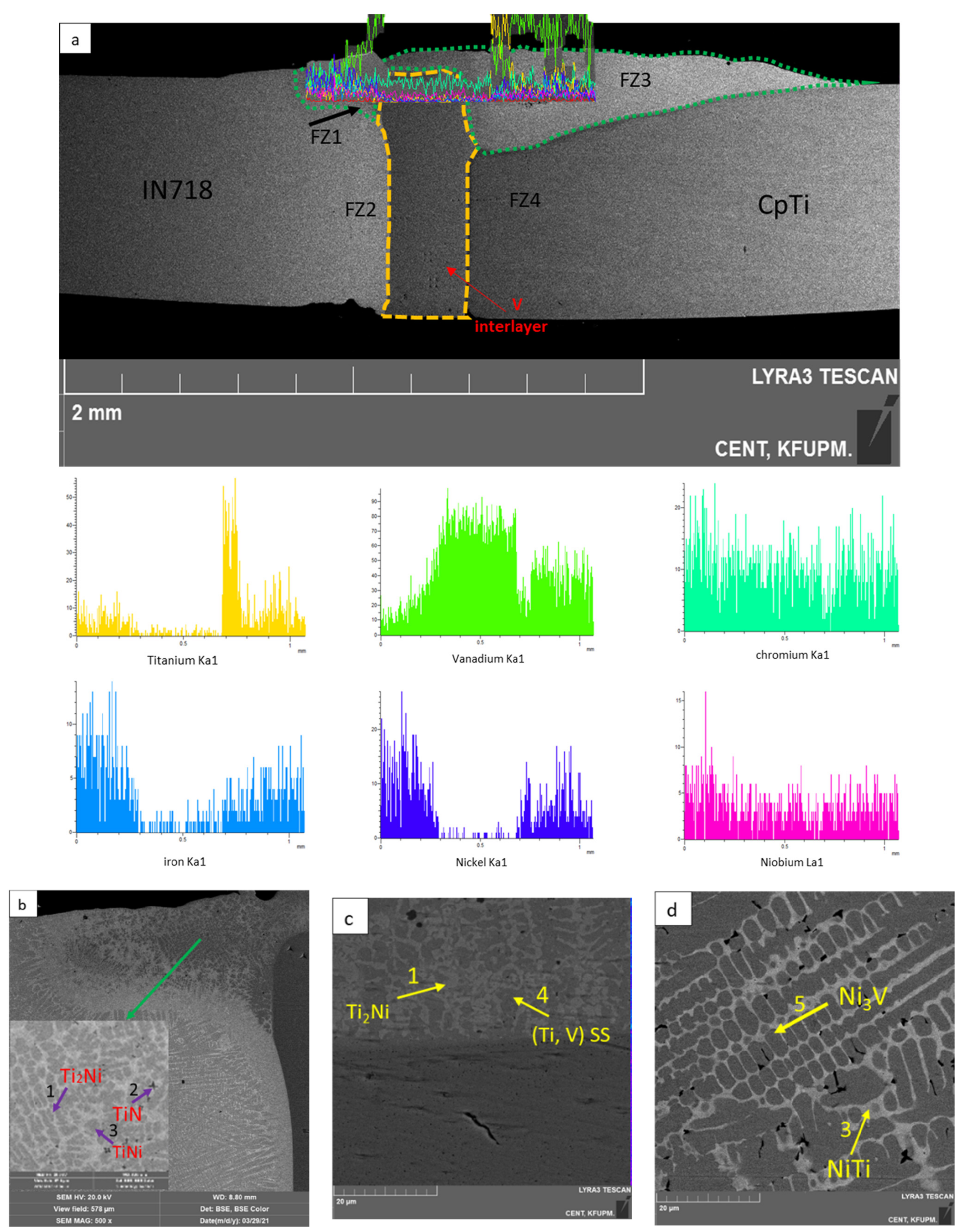
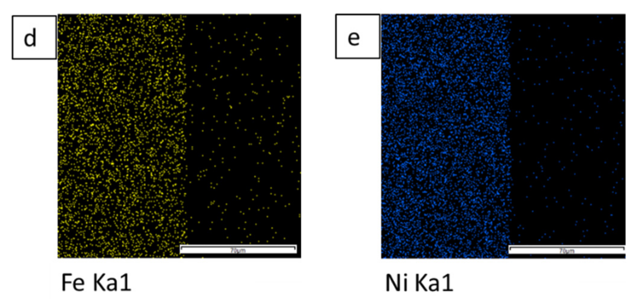
3.1. Microstructural Characterization
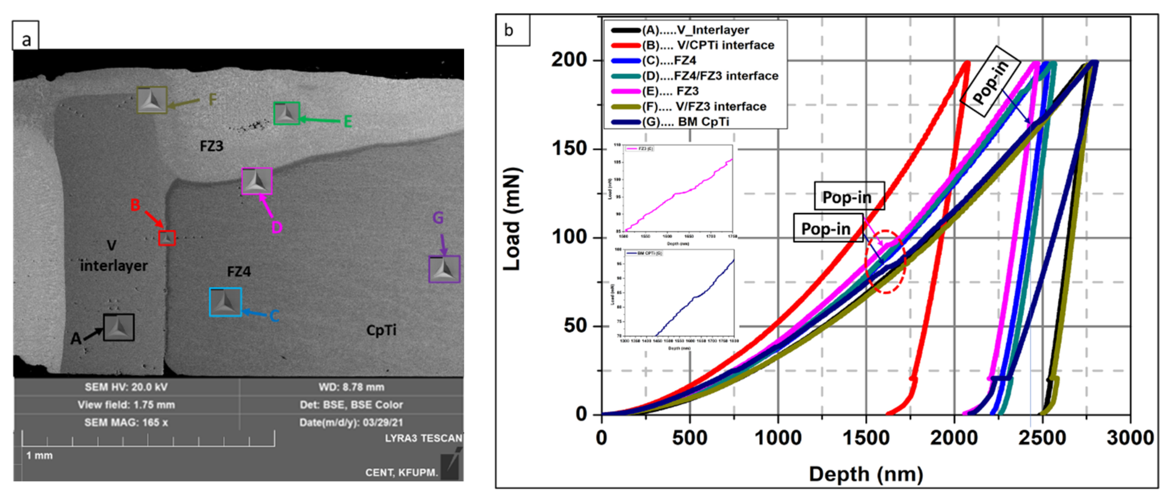
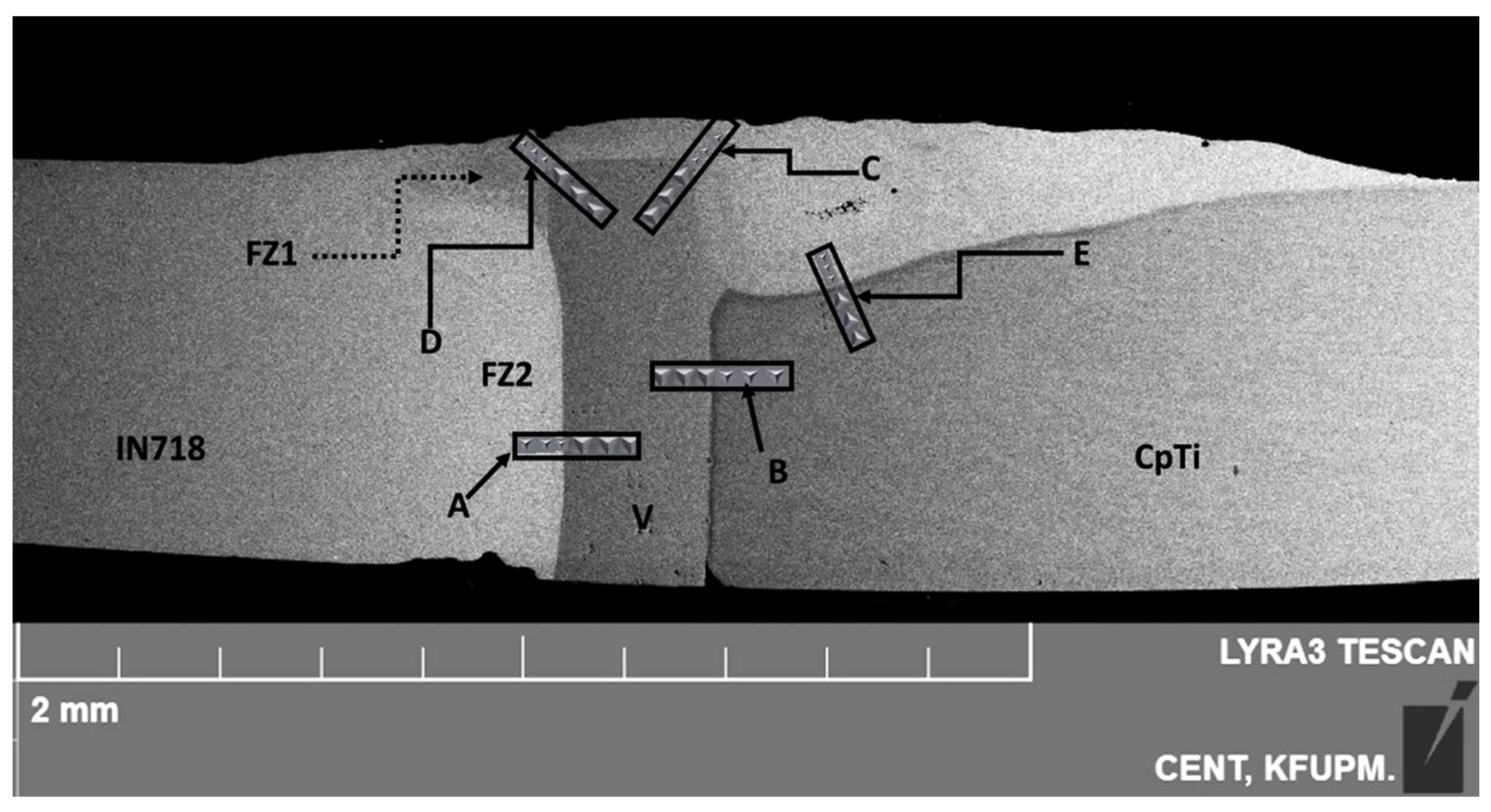
3.2. Nanoindentation
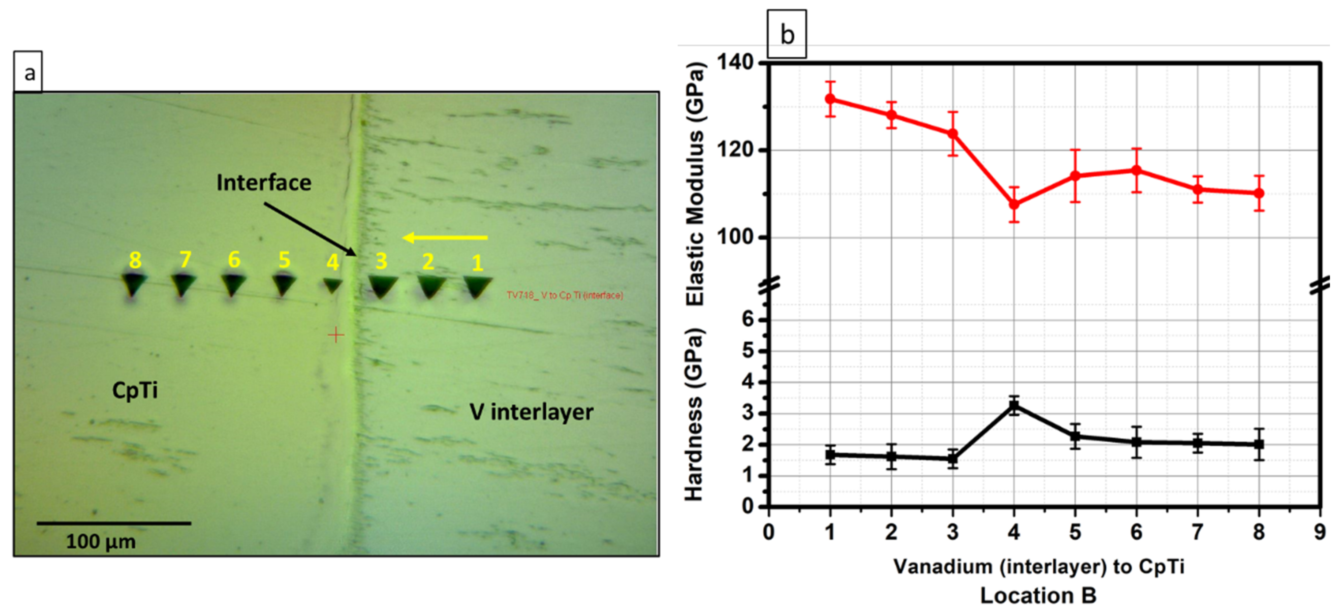
3.2.1. CpTi and the Vanadium Interlayer Side
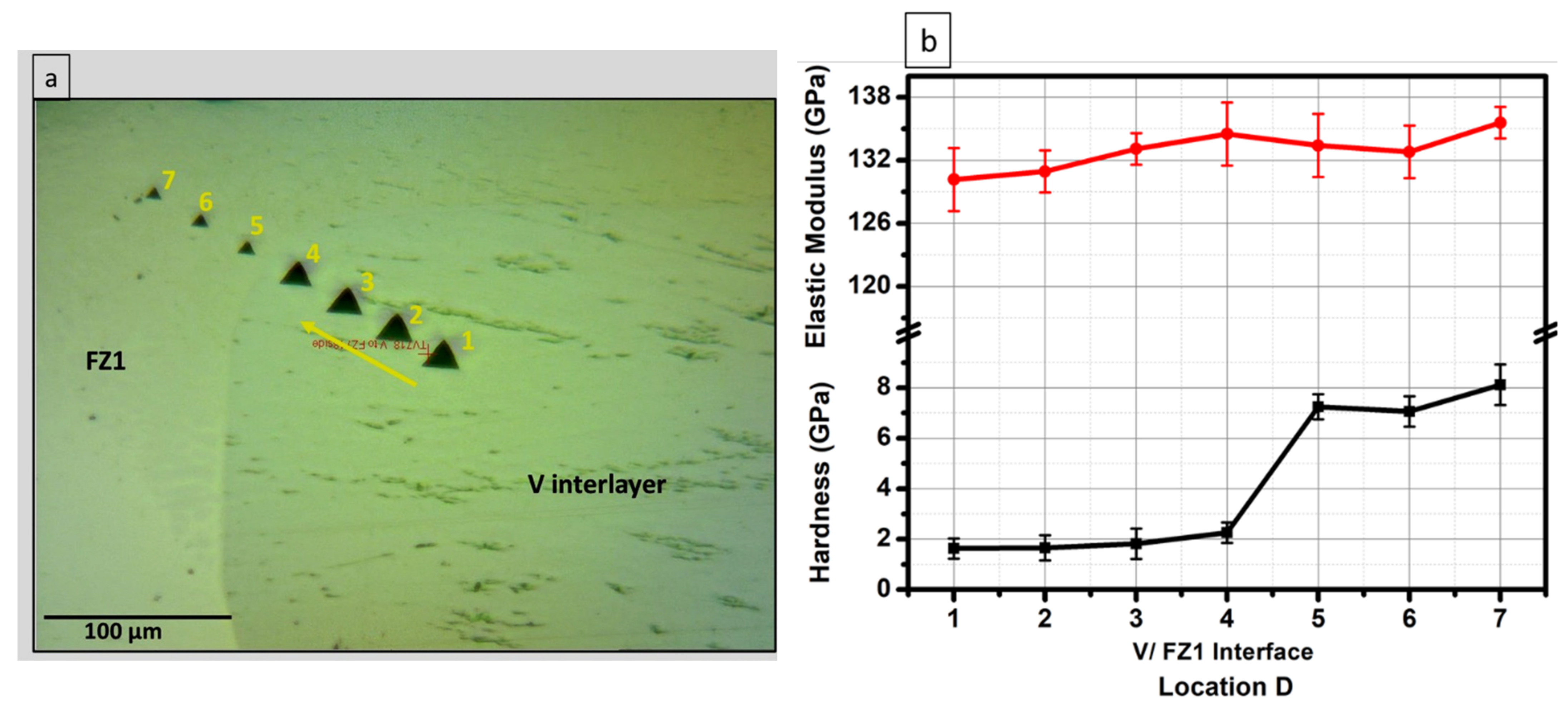
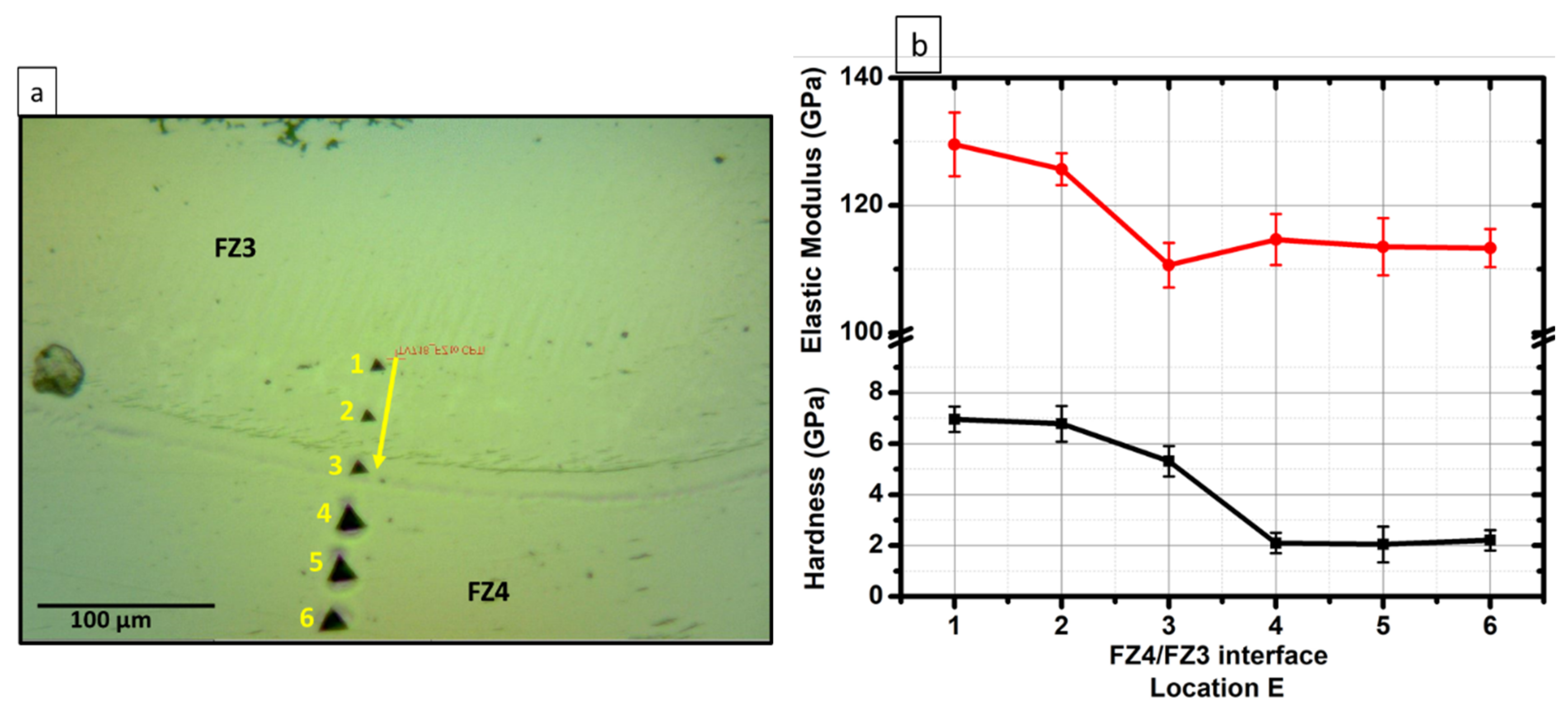
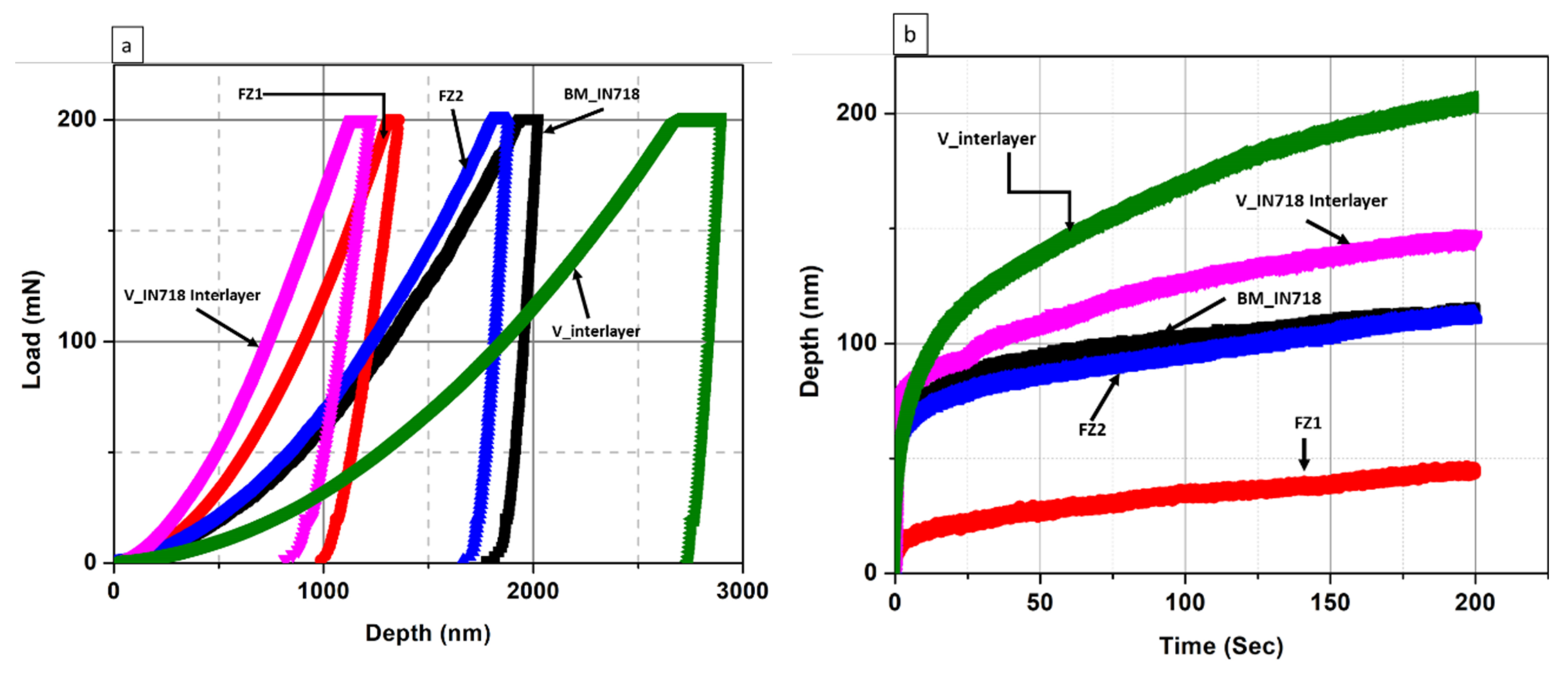
3.2.2. IN718 and the Vanadium Interlayer Side
3.3. Nanohardness Line Scan
3.4. Mechanical Properties Mapping
3.5. Nano Creep
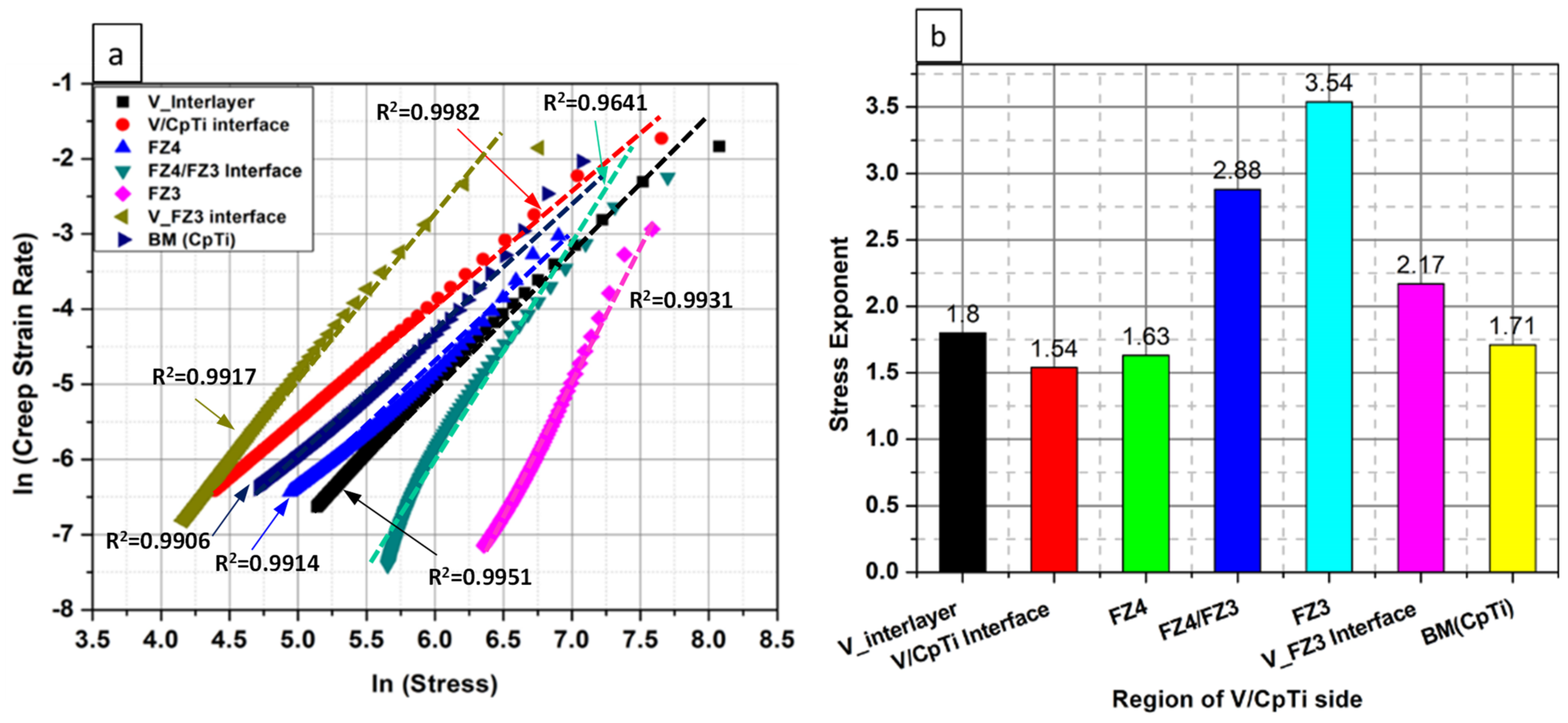
3.5.1. V/CpTi Side
3.5.2. V/IN718 Side
3.5.3. Creep Discussions
4. Conclusions
Author Contributions
Funding
Data Availability Statement
Acknowledgments
Conflicts of Interest
References
- Mabuwa, S.; Msomi, V.; Muribwathoho, O.; Motshwanedi, S.S. The microstructure and mechanical properties of the friction stir processed TIG-welded aerospace dissimilar aluminium alloys. Mater. Today Proc. 2021, 46, 658–664. [Google Scholar] [CrossRef]
- Kumar, S.; Sirohi, S.; Vidyarthy, R.; Gupta, A.; Pandey, C. Role of the Ni-based filler composition on microstructure and mechanical behavior of the dissimilar welded joint of P22 and P91 steel. Int. J. Press. Vessel. Pip. 2021, 193, 104473. [Google Scholar] [CrossRef]
- Shehabeldeen, T.A.; El-Shafai, N.M.; El-Mehasseb, I.M.; Yin, Y.; Ji, X.; Shen, X.; Zhou, J. Improvement of microstructure and mechanical properties of dissimilar friction stir welded aluminum/titanium joints via aluminum oxide nanopowder. Vacuum 2021, 188, 110216. [Google Scholar] [CrossRef]
- Rinne, J.; Seffer, O.; Nothdurft, S.; Hermsdorf, J.; Kaierle, S.; Overmeyer, L. Investigations on the weld metal composition and associated weld metal cracking in laser beam welded steel copper dissimilar joints. J. Mater. Process. Technol. 2021, 296, 117178. [Google Scholar] [CrossRef]
- Argesi, F.B.; Shamsipur, A.; Mirsalehi, S.E. Preparation of bimetallic nano-composite by dissimilar friction stir welding of copper to aluminum alloy. Trans. Nonferrous Met. Soc. China 2021, 31, 1363–1380. [Google Scholar] [CrossRef]
- Ghiban, B.; Elefterie, C.F.; Guragata, C.; Bran, D. Requirements of Inconel 718 alloy for aeronautical applications. Int. Conf. Struct. Anal. Adv. Mater. Icsaam 2017 2018, 1932, 030016. [Google Scholar] [CrossRef]
- Ola, O.; Doern, F. A study of cold metal transfer clads in nickel-base INCONEL 718 superalloy. Mater. Des. 2014, 57, 51–59. [Google Scholar] [CrossRef]
- Majeed, T.; Mehta, Y.; Siddiquee, A.N. Challenges in joining of unequal thickness materials for aerospace applications: A review. Proc. Inst. Mech. Eng. Part L J. Mater. Des. Appl. 2021, 235, 934–945. [Google Scholar] [CrossRef]
- Nirudhoddi, B.S.; Prasad, K.S.; Vivek, A.; Daehn, G.S. High strength welds in titanium & nickel based alloys by impact welding—A practical method. J. Adv. Join. Process. 2021, 3, 100056. [Google Scholar] [CrossRef]
- Fang, Y.-J.; Jiang, X.-S.; Mo, D.-F.; Song, T.; Shao, Z.-Y.; Zhu, D.-G.; Zhu, M.-H.; Luo, Z.-P. Microstructure and Mechanical Properties of Electron Beam-Welded Joints of Titanium TC4 (Ti-6Al-4V) and Kovar (Fe-29Ni-17Co) Alloys with Cu/Nb Multi-Interlayer. Adv. Mater. Sci. Eng. 2018, 2018, 2042871. [Google Scholar] [CrossRef] [Green Version]
- Min, K. Information to Users Umi, Dissertation, vol. no. Structural Biology and Molecular Biophysics. Ph.D. Thesis, University of Pennsylvania, Philadelphia, PA, USA, 1995. [Google Scholar]
- Corigliano, P.; Crupi, V. Fatigue analysis of TI6AL4V/INCONEL 625 dissimilar welded joints. Ocean Eng. 2021, 221, 108582. [Google Scholar] [CrossRef]
- Seretsky, J.; Ryba, E.R. Laser Welding of Dissimilar Metals: Titanium to Nickel; Welding Research Supplement: Miami, FL, USA, 1976. [Google Scholar]
- Chen, H.-C.; Pinkerton, A.; Li, L. Fibre laser welding of dissimilar alloys of Ti-6Al-4V and Inconel 718 for aerospace applications. Int. J. Adv. Manuf. Technol. 2011, 52, 977–987. [Google Scholar] [CrossRef]
- Chatterjee, S.; Abinandanan, T.; Chattopadhyay, K. Microstructure development during dissimilar welding: Case of laser welding of Ti with Ni involving intermetallic phase formation. J. Mater. Sci. 2006, 41, 643–652. [Google Scholar] [CrossRef]
- Fuji, A.; Horiuchi, Y.; Yamamoto, K. Friction welding of pure titanium and pure nickel. Sci. Technol. Weld. Join. 2005, 10, 287–294. [Google Scholar] [CrossRef]
- Chatterjee, S.; Abinandanan, T.; Chattopadhyay, K. Phase formation in Ti/Ni dissimilar welds. Mater. Sci. Eng. A 2008, 490, 7–15. [Google Scholar] [CrossRef]
- Gao, X.-L.; Liu, J.; Zhang, L.-J. Effect of heat input on microstructure and mechanical properties of pulsed laser welded joints in Ti6Al4V/Nb dissimilar alloys. Int. J. Adv. Manuf. Technol. 2017, 94, 3937–3947. [Google Scholar] [CrossRef]
- Liu, J.; Liu, H.; Gao, X.-L.; Yu, H. Microstructure and mechanical properties of laser welding of Ti6Al4V to Inconel 718 using Nb/Cu interlayer. J. Mater. Process. Technol. 2020, 277, 116467. [Google Scholar] [CrossRef]
- Ogura, T.; Miyoshi, K.; Matsumura, T.; Imai, T.; Saida, K. Improvement of joint strength in dissimilar friction welding of Ti-6Al-4V alloy to type-718 nickel-based alloy using the Au–Ni interlayer. Sci. Technol. Weld. Join. 2018, 24, 327–333. [Google Scholar] [CrossRef]
- Klueh, R.L.; King, J.F.; Griffith, L.J. Simple Test for Dissimilar-Metal Welds; Welding Research Supplement: Miami, FL, USA, 1983. [Google Scholar]
- Hepworth, J. The effect of residual stress on the creep deformation of welded pipe. Int. J. Press. Vessel. Pip. 1984, 15, 271–290. [Google Scholar] [CrossRef]
- McKeen, L.W. The Effect of Creep and Other Time Related Factors on Plastics and Elastomers, 2nd ed.; Elsevier: Oxford, UK, 2015. [Google Scholar]
- Li, W.; Henshall, J.; Hooper, R.; Easterling, K. The mechanisms of indentation creep. Acta Met. Mater. 1991, 39, 3099–3110. [Google Scholar] [CrossRef]
- Schuh, C.A. Nanoindentation Opportunities for Future Scientific Inquiry. Mater. Today 2006, 9, 32–40. [Google Scholar] [CrossRef]
- Ma, Z.; Long, S.; Pan, Y.; Zhou, Y. Loading rate sensitivity of nanoindentation creep in polycrystalline Ni films. J. Mater. Sci. 2008, 43, 5952–5955. [Google Scholar] [CrossRef] [Green Version]
- Hu, J.; Sun, G.; Zhang, X.; Wang, G.; Jiang, Z.; Han, S.; Zhang, J.; Lian, J. Effects of loading strain rate and stacking fault energy on nanoindentation creep behaviors of nanocrystalline Cu, Ni-20 wt.%Fe and Ni. J. Alloys Compd. 2015, 647, 670–680. [Google Scholar] [CrossRef]
- Nguyen, N.-V.; Pham, T.-H.; Kim, S.-E. Microstructure and strain rate sensitivity behavior of SM490 structural steel weld zone investigated using indentation. Constr. Build. Mater. 2019, 206, 410–418. [Google Scholar] [CrossRef]
- Nguyen, N.-V.; Pham, T.-H.; Kim, S.-E. Strain rate sensitivity behavior of a structural steel during low-cycle fatigue investigated using indentation. Mater. Sci. Eng. A 2019, 744, 490–499. [Google Scholar] [CrossRef]
- Gao, Z.; Song, Y.; Pan, Z.; Chen, J.; Ma, Y. Nanoindentation investigation on the creep behavior of P92 steel weld joint after creep-fatigue loading. Int. J. Fatigue 2020, 134, 105506. [Google Scholar] [CrossRef]
- Song, Y.; Huang, X.; Gao, Z.; Li, X.; Ma, Y. Nanoindentation creep behavior of RPV’s weld joint at room temperature. Mech. Time Depend. Mater. 2020, 24, 253–263. [Google Scholar] [CrossRef]
- Oliver, W.C.; Pharr, G.M. An improved technique for determining hardness and elastic modulus using load and displacement. J. Mater. Res. 1992, 1, 1564–1583. [Google Scholar] [CrossRef]
- Poisl, W.; Oliver, W.; Fabes, B. The relationship between indentation and uniaxial creep in amorphous selenium. J. Mater. Res. 1995, 10, 2024–2032. [Google Scholar] [CrossRef]
- Liu, X.; Zhang, Q.; Zhao, X.; Yang, X.; Luo, L. Ambient-temperature nanoindentation creep in ultrafine-grained titanium processed by ECAP. Mater. Sci. Eng. A 2016, 676, 73–79. [Google Scholar] [CrossRef]
- Lucas, B.N.; Oliver, W.C. Indentation power-law creep of high-purity indium. Met. Mater. Trans. A 1999, 30, 601–610. [Google Scholar] [CrossRef]
- Su, C.; Herbert, E.G.; Sohn, S.; LaManna, J.A.; Oliver, W.C.; Pharr, G.M. Measurement of power-law creep parameters by instrumented indentation methods. J. Mech. Phys. Solids 2013, 61, 517–536. [Google Scholar] [CrossRef]
- Massalski, T.; Subramanian, P.R. Binary Alloy Phase Diagrams. In Alloy. Phase Diagrams; ASM International: Almere, The Netherlands, 2018; p. 89. [Google Scholar]
- Liu, W.; Cai, Q.; Ma, Y.; Wang, Y.; Liu, H.; Li, D. Microstructure and mechanical properties of diffusion bonded W/steel joint using V/Ni composite interlayer. Mater. Charact. 2013, 86, 212–220. [Google Scholar] [CrossRef]
- Zoeram, A.S.; Mousavi, S.A. Laser welding of Ti–6Al–4V to Nitinol. Mater. Des. 2014, 61, 185–190. [Google Scholar] [CrossRef]
- Pöhl, F. Pop-in behavior and elastic-to-plastic transition of polycrystalline pure iron during sharp nanoindentation. Sci. Rep. 2019, 9, 1–12. [Google Scholar] [CrossRef] [Green Version]
- Lan, H.; Venkatesh, T. On the relationships between hardness and the elastic and plastic properties of isotropic power-law hardening materials. Philos. Mag. 2013, 94, 35–55. [Google Scholar] [CrossRef]
- Luo, L.; Zhao, X.; Liu, X.; Yang, X. Creep Behavior of UFG CP Ti at Room Temperature. IOP Conf. Series Mater. Sci. Eng. 2017, 250, 12062. [Google Scholar] [CrossRef]
- Mahmudi, R.; Pourmajidian, M.; Geranmayeh, A.; Gorgannejad, S.; Hashemizadeh, S. Indentation creep of lead-free Sn–3.5Ag solder alloy: Effects of cooling rate and Zn/Sb addition. Mater. Sci. Eng. A 2013, 565, 236–242. [Google Scholar] [CrossRef]
- Bolshakov, A.; Pharr, G.M. Influences of pileup on the measurement of mechanical properties by load and depth sensing indentation techniques. J. Mater. Res. 1998, 13, 1049–1058. [Google Scholar] [CrossRef]
- Saha, R.; Nix, W. Soft films on hard substrates—nanoindentation of tungsten films on sapphire substrates. Mater. Sci. Eng. A 2001, 319–321, 898–901. [Google Scholar] [CrossRef]
- Salari, S.; Rahman, S.; Polycarpou, A.A.; Beheshti, A. Elevated temperature mechanical properties of Inconel 617 surface oxide using nanoindentation. Mater. Sci. Eng. A 2020, 788, 139539. [Google Scholar] [CrossRef]
- Van Swygenhoven, H.; Derlet, P.M. Grain-boundary sliding in nanocrystalline fcc metals. Phys. Rev. B 2001, 64, 224105. [Google Scholar] [CrossRef]
- Sauthoff, G. Creep of intermetallics. Mater. Sci. Technol. 1992, 8, 363–366. [Google Scholar] [CrossRef]
- Kihara, S.; Newkirk, J.B.; Ohtomo, A.; Saiga, Y. Morphological changes of carbides during creep and their effects on the creep properties of inconel 617 at 1000 °C. Met. Mater. Trans. A 1980, 11, 1019–1031. [Google Scholar] [CrossRef]
- Viguier, B. Dislocation densities and strain hardening rate in some intermetallic compounds. Mater. Sci. Eng. A 2003, 349, 132–135. [Google Scholar] [CrossRef]
- Song, J.-M.; Shen, Y.-L.; Su, C.-W.; Lai, Y.-S.; Chiu, Y.-T. Strain Rate Dependence on Nanoindentation Responses of Interfacial Intermetallic Compounds in Electronic Solder Joints with Cu and Ag Substrates. Mater. Trans. 2009, 50, 1231–1234. [Google Scholar] [CrossRef] [Green Version]
- El-Bediwi, A.; Lashin, A.; Mossa, M.; Kamal, M. Indentation creep and mechanical properties of quaternary Sn–Sb based alloys. Mater. Sci. Eng. A 2011, 528, 3568–3572. [Google Scholar] [CrossRef]


| Elements | IN718 | CpTi | V |
|---|---|---|---|
| Al | 0.88 | - | - |
| Ti | 1.02 | Bal. | - |
| Cr | 21.75 | - | - |
| Fe | 18.61 | 0.15 | - |
| V | - | - | 100 |
| Ni | 50.75 | - | - |
| Nb | 5.29 | - | - |
| Mo | 1.61 | - | - |
| Co | 0.09 | - | - |
| C | - | 0.04 | - |
| O | - | 0.15 | - |
| Spot | V | Fe | Ni | Cr | Ti | Nb | N | Possible Phase |
|---|---|---|---|---|---|---|---|---|
| 1 | 16.14 | 7.16 | 30.27 | 2.98 | 43.44 | Ti2Ni | ||
| 2 | 5.34 | 1.92 | 8.69 | 0.94 | 56.44 | 1.62 | 25.06 | TiN |
| 3 | 27.51 | 4.79 | 36.97 | 1.73 | 23.15 | 5.85 | NiTi | |
| 4 | 31.22 | 3.65 | 8.17 | 3.87 | 53.10 | SS (Ti, V) BCC Phase | ||
| 5 | 69.57 | 6.98 | 8.82 | 10.37 | 4.26 | NiV3 |
Publisher’s Note: MDPI stays neutral with regard to jurisdictional claims in published maps and institutional affiliations. |
© 2021 by the authors. Licensee MDPI, Basel, Switzerland. This article is an open access article distributed under the terms and conditions of the Creative Commons Attribution (CC BY) license (https://creativecommons.org/licenses/by/4.0/).
Share and Cite
Shehbaz, T.; Khan, F.N.; Junaid, M.; Haider, J. Investigating Nanoindentation Creep Behavior of Pulsed-TIG Welded Inconel 718 and Commercially Pure Titanium Using a Vanadium Interlayer. Metals 2021, 11, 1492. https://doi.org/10.3390/met11091492
Shehbaz T, Khan FN, Junaid M, Haider J. Investigating Nanoindentation Creep Behavior of Pulsed-TIG Welded Inconel 718 and Commercially Pure Titanium Using a Vanadium Interlayer. Metals. 2021; 11(9):1492. https://doi.org/10.3390/met11091492
Chicago/Turabian StyleShehbaz, Tauheed, Fahd Nawaz Khan, Massab Junaid, and Julfikar Haider. 2021. "Investigating Nanoindentation Creep Behavior of Pulsed-TIG Welded Inconel 718 and Commercially Pure Titanium Using a Vanadium Interlayer" Metals 11, no. 9: 1492. https://doi.org/10.3390/met11091492