Article

Effect of Oxygen Flow Rate on Properties of Aluminum-Doped Indium-Saving Indium Tin Oxide (ITO) Thin Films Sputtered on Preheated Glass Substrates

1
National Academy of Science of Ukraine, Frantsevich Institute for Problems of Materials Science, 3, Krzhyzhanovski Str., 03142 Kyiv, Ukraine
2
National Academy of Science of Ukraine, Physico-Technological Institute of Metals and Alloys, 34/1 Vernadsky Ave., 03142 Kyiv, Ukraine
3
Institute of Multidisciplinary Research for Advanced Materials, Tohoku University, 2-1-1, Katahira, Aoba-ku, Sendai 980-8577, Japan
*
Author to whom correspondence should be addressed.
Metals 2021, 11(10), 1604; https://doi.org/10.3390/met11101604
Submission received: 4 September 2021 / Revised: 28 September 2021 / Accepted: 2 October 2021 / Published: 9 October 2021

Abstract

:
Amorphous aluminum-doped indium tin oxide (ITO) thin films with a reduced indium oxide content of 50 mass% were manufactured by co-sputtering of ITO and Al2O3 targets in a mixed argon–oxygen atmosphere onto glass substrates preheated at 523 K. The oxygen gas flow rate and heat treatment temperature effects on the electrical, optical and structural properties of the films were studied. Thin films were characterized by means of a four-point probe, ultraviolet–visible-infrared (UV–Vis-IR) spectroscopy and X-ray diffraction. Transmittance of films and crystallization temperature increased as a result of doping of the ITO thin films by aluminum. The increase in oxygen flow rate led to an increase in transmittance and hindering of the crystallization of the aluminum-doped indium saving ITO thin films. It has been found that the film sputtered under optimal conditions showed a volume resistivity of 713 µΩ cm, mobility of 30.8 cm2/V·s, carrier concentration of 2.9 × 1020 cm−3 and transmittance of over 90% in the visible range.

1. Introduction

Thin films of indium tin oxide (ITO) have been extensively used in numerous applications such as semiconducting window electrodes for solar cells, transparent conducting electrodes for panel displays, optical solar reflectors, etc., [1,2,3,4,5] due to their low resistivity and high optical transmittance in the visible range.
However, ITO thin films have a high price due to their high demand in industry and limited indium natural reserves. Therefore, indium-saving ITO thin films which maintain ITO’s electrical and optical properties, as well as being cost-effective, have been investigated in recent years [6,7,8,9,10,11,12]. In order to improve optoelectronic properties of the indium-saving ITO thin films, the latter were doped with different oxides [13,14,15]. This allowed the achievement of low resistivity and high transmittance in the visible range and made indium-saving ITO thin films doped with titanium, iron and aluminum an alternative to conventional ITO (In2O3–10 mass% SnO2). It was shown that the optimal RF sputtering power for the Al2O3 target WRF for the deposition of aluminum-doped indium-saving ITO thin films was 40 W.
In this study, oxygen flow rate and heat treatment effect on the optical, electrical and structural properties of amorphous aluminum-doped indium-saving ITO (In2O3–50 mass% SnO2, ITO50) thin films produced by a co-sputtering method onto glass substrates preheated at 523 K (ITO50:Al2O3 (PHS)) was studied. In order to reduce indium usage in ITO films, the amount of indium oxide in the target was decreased from 90 mass% to 50 mass%.

2. Materials and Methods

Aluminum-doped ITO50 (ITO50:Al2O3) thin films were prepared by using a commercial sputtering system (ULVAC, CS-200).
ITO50 (Mitsui Mining & Smelting, In2O3–48.9 mass% SnO2) and Al2O3 (Kojundo Chemical Laboratory, 99.99 mass%) targets were co-sputtered. The DC plasma power for the ITO50 target was kept at 100 W and the RF plasma power for the Al2O3 target was set at 40 W. The amorphous aluminum-doped ITO50 thin films were sputtered onto glass substrates (Corning EAGLE 2000, Alkaline Earth Boro-Aluminosilicate glass, surface: 50 mm × 50 mm, thickness: 0.7 mm) preheated at 523 K (PHS) under the rotation of the substrate holder in order to obtain a homogeneous deposition. The argon flow rate was kept constant at Q(Ar) = 50 sccm while the oxygen flow rate Q(O2) was altered between 0–0.6 sccm, and the deposition time was fixed at 30 min.
The deposited films were heat-treated (HT) in air at 523–923 K for 60 min and cooled at room temperature. Optoelectronic properties of thin films were determined for both as-deposited (as-depo.) and heat-treated (HT) conditions. Optical transmittance τ was measured in the wavelength range of 200–2600 nm using a spectrophotometer (U-4100, Hitachi High-Tech, Tokyo, Japan) Volume resistivity ρv was measured with a resistivity meter (Loresta GP Model MCP-T610, Mitsubishi chemical analytech, Kanagawa, Japan) by using a 4-terminal [16]. The crystallinities of the films for different HT temperatures (523–823 K) were obtained from their X-ray diffraction (XRD) measurements using an X-ray diffractometer (Rint-2000, Rigaku, Yamanashi, Japan) with Cu-Kα (0.15418 nm) radiation. Surface analysis was taken using a scanning probe microscope (SPM, L-trace II, SII, Tokyo, Japan) under the DFM.

3. Results

3.1. Deposition Rate

Table 1 presents the thickness and deposition rate of the ITO50:Al2O3 (PHS) thin films at different oxygen flow rates. It was found that the thickness and deposition rate decreased with increasing Q(O2). The thickness and deposition rate of the ITO50:Al2O3 (PHS) thin films at different oxygen flow rates have a similar dependence as the undoped ITO50 thin films [12]. The deposition parameters (d and rdep) declined sharply in ranges of Q(O2) from 0 to 0.1 sccm and from 0.4 to 0.6 sccm, while over a range of oxygen flow rates between 0.1 and 0.4 sccm, they remained constant within standard deviation (Table 1). Film-thickness drop at increasing of Q(O2) could be explained by the decrease in the mean free path of the atoms [17].

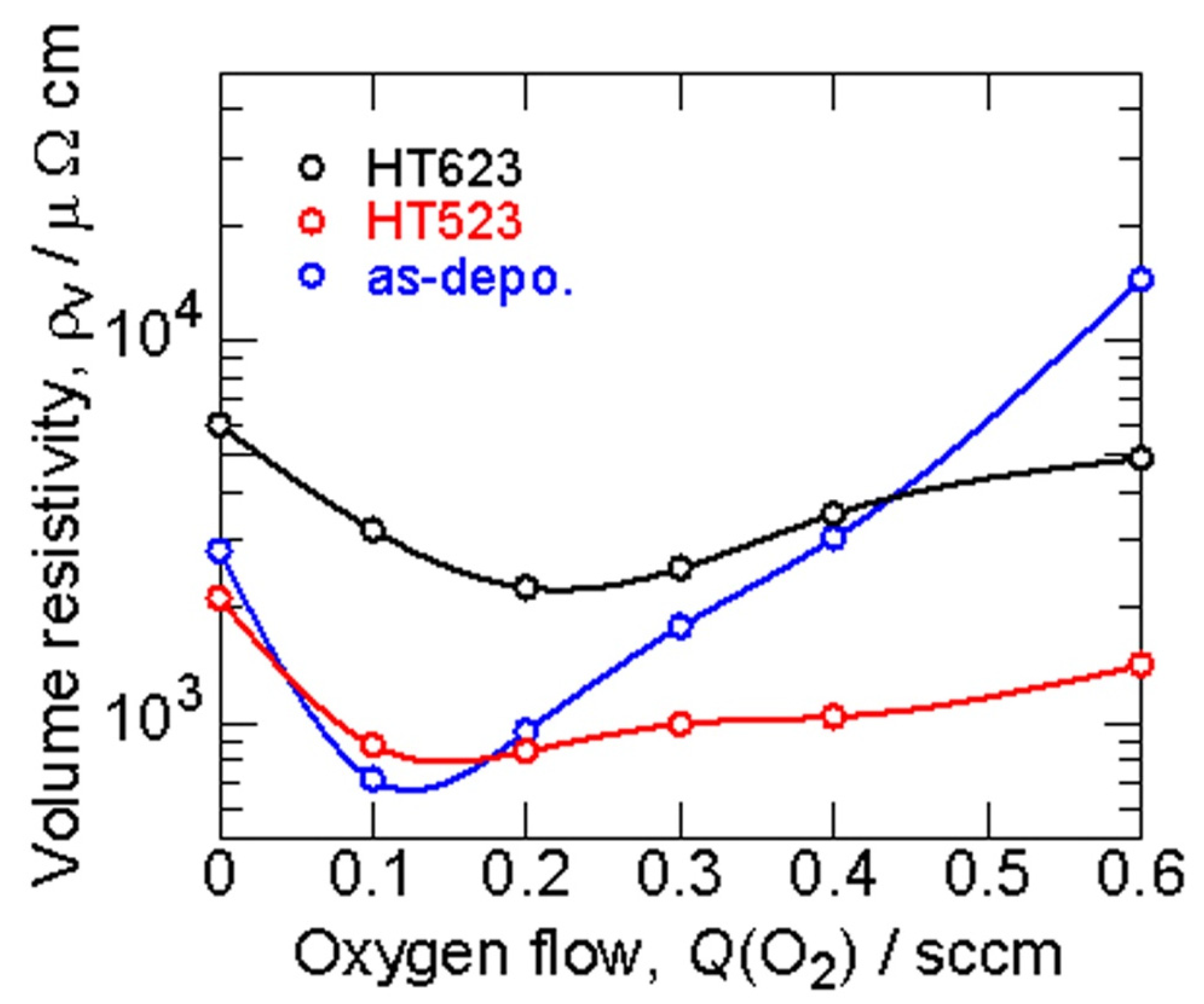
3.2. Optical and Electrical Properties

Figure 1 shows the effects of Q(O2) and heat treatment temperature on the volume resistivity ρv measured for the ITO50:Al2O3 (PHS) thin films.
The ρv of the ITO50:Al2O3 (PHS) thin films depends on the Q(O2). The ρv of the as-depo. ITO50:Al2O3 (PHS) thin films decreased with increasing Q(O2), showing minimal values at Q(O2) = 0.1 sccm (713 μΩ cm) and then increasing. The volume resistivity of the as-depo. ITO50:Al2O3 (PHS) thin films sputtered at Q(O2) = 0.1 sccm was lower than that of undoped ITO50 thin films sputtered under the same Q(O2) (66800 μΩ cm) [12,15]. The main charge carriers in ITO thin films are electrons that are created by the ionization of oxygen vacancies and tin substitution at indium sites. In this study, the concentration of tin was constant. Thus, for the as-depo. ITO50:Al2O3 (PHS) thin films, the oxygen vacancy density decreased with increasing Q(O2) (Figure 2b).
The ρv of the ITO50:Al2O3 (PHS) thin films after heat treatment at 523 K (HT523) decreased with increasing Q(O2) up to 0.2 sccm due to increasing electron mobility (Figure 2a), and then increased with decreasing electron mobility (Figure 2a). The carrier density of the НT523 ITO50:Al2O3 (PHS) thin films increased to 2.4 × 1020 cm−3 with increasing Q(O2) up to 0.1 sccm, and then decreased (Figure 2b). In general, the carrier density showed high values over the whole range of Q(O2). When the HT temperature was increased above 523 K, ρv increased due to the filling of oxygen vacancies by chemisorption of oxygen on the film surface at high temperatures during heat treatment in air [18]; this effect can be easily seen in Figure 1 when the heat treatment temperature rises to 623 K.
Figure 3 presents the UV–vis-IR transmittance τ spectra of the as-depo. and HT523 ITO50:Al2O3 (PHS) thin films for different Q(O2).
Figure 3a shows that the τ of the as-depo. ITO50:Al2O3 (PHS) films increased with increasing Q(O2). With increasing Q(O2) over 0.1 sccm, the τ of the ITO50:Al2O3 (PHS) films did not change significantly in the visible range, while in the short-wavelength infrared region, the τ increased with increasing Q(O2). The same tendency was observed for the HT523 ITO50:Al2O3 (PHS) films (Figure 3b). It worth mentioning that heat treatment at 523 K led to an increase in τ. Comparison of transmittance curves of the ITO50:Al2O3 (PHS) film and ITO50 (PHS) thin film deposited at Q(O2) = 0.1 sccm showed significant increases in τ when the ITO50 thin film was doped with Al2O3, since aluminum oxide is an additional source of oxygen during filling of oxygen vacancies. The same tendency was observed for iron-doped indium-saving ITO thin films [14].

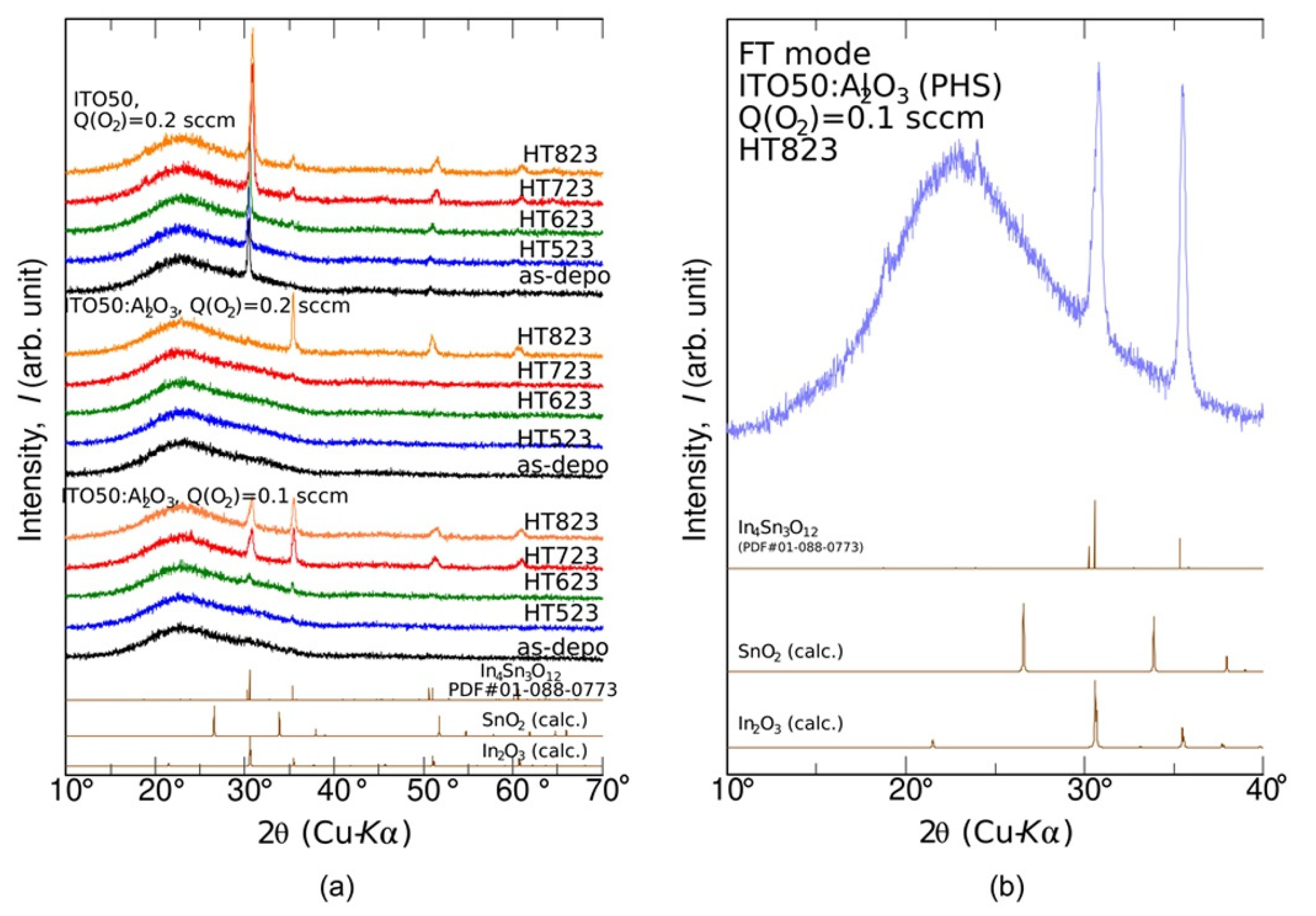
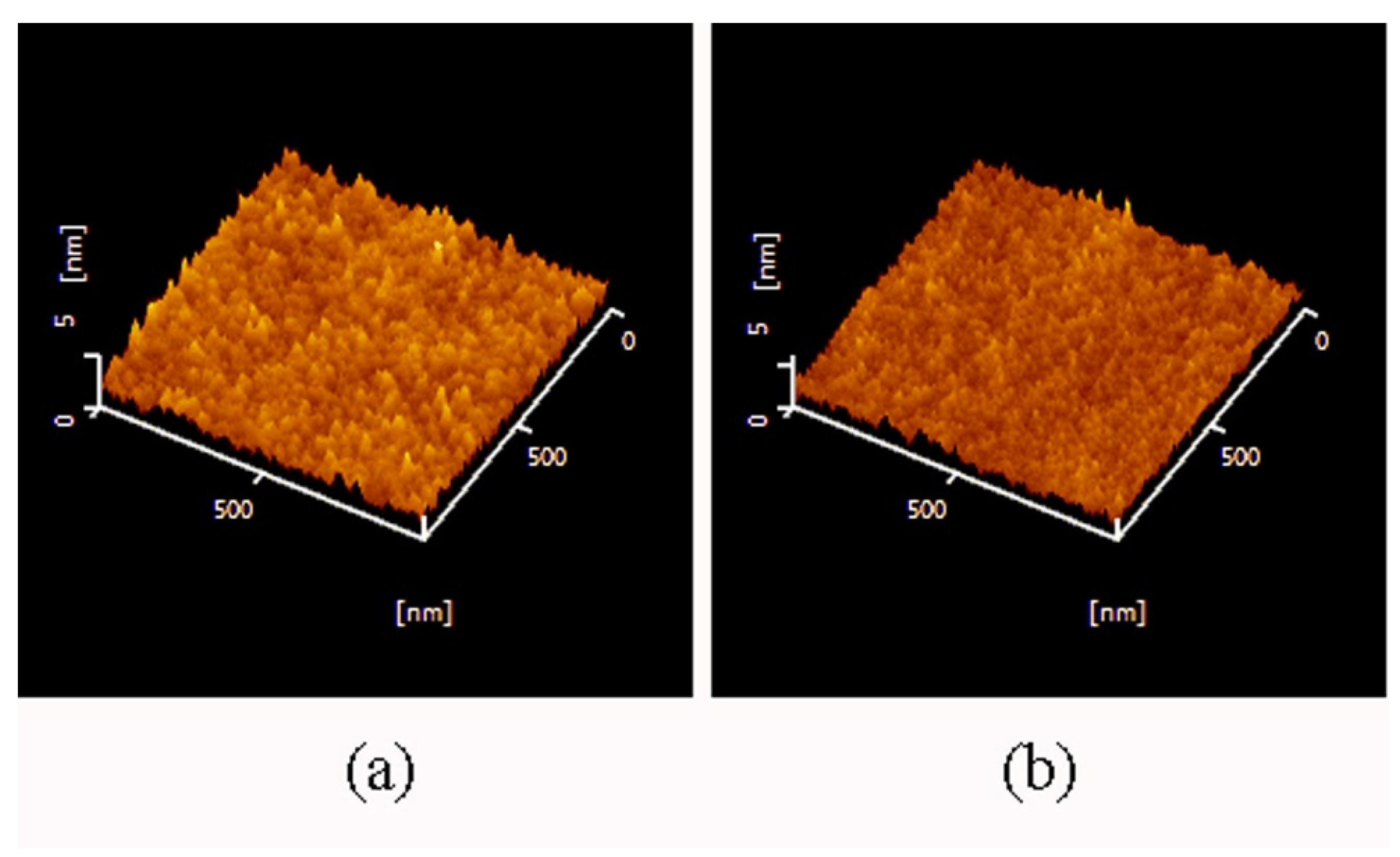
3.3. Structural Properties

The X-ray diffractometer (XRD) patterns for the typical as-depo. and HT523-823 ITO50:Al2O3 (PHS) thin films sputtered under two different Q(O2),had the standard reference patterns of In4Sn3O12, In2O3, and SnO2, as shown in Figure 4a.
As follows from Figure 4a, the as-depo. ITO50:Al2O3 (PHS) films sputtered at Q(O2) = 0.1 and 0.2 sccm were amorphous. The hump between 2θ = 15° and 35° is owing to the background of the glass substrates. The XRD pattern of ITO50:Al2O3 (PHS) films sputtered at Q(O2) = 0.1 sccm showed small peaks after heat treatment at 623 K (HT623), while thin films deposited at Q(O2) = 0.2 sccm revealed sharp peaks after heat treatment at 823 K (HT823). Thus, increasing the Q(O2) during sputtering of ITO50:Al2O3 (PHS) films leads to increasing crystallization temperature. The main peaks of the measured patterns for the ITO50:Al2O3 (PHS) films can be assigned to In4Sn3O12 (Figure 4b) [19,20]. Rhombohedral indium tin oxide In4Sn3O12 shows the peaks at 18.9°, 22.95°, 23.98° (Figure 4b, peaks are shown by dashed lines), which is different from the positions of peaks in the standard cubic indium oxide In2O3 compound. Aluminum oxide or any other secondary impurities were not revealed in the observed XRD patterns. The same tendency was observed for iron-doped ITO50 thin films [15].
XRD results for the as-depo. and HT523-823 ITO50:Al2O3 (PHS) films deposited at WRF(Al2O3) = 40 W, Q(O2) = 0.2 sccm were compared with those of ITO50 (PHS) thin films sputtered at the same Q(O2) (Figure 4a). As follows from Figure 4a, the as-deposited film is amorphous in contrast to crystallized undoped ITO50 thin film deposited at the same oxygen flow rate. As can be seen from this comparison, doping with aluminum oxide hindered the crystallization of thin films, and only after heat treatment at temperatures above 723 K did the aluminum-doped films deposit at Q(O2) = 0.2 sccm crystallize (Figure 4a).
Surface analysis results for the as-deposited and HT923 ITO50:Al2O3 (PHS) thin films are presented in Figure 5.
Both as-deposited and heat-treated thin films have a smooth surface morphology. The root mean square height (Sq) and arithmetical mean height (Sa) of ITO:Al2O3(PHS) thin films in comparison with ITO90 and ITO50 thin films sputtered under optimal conditions are presented in Table 2.
As can be seen from Table 2, heat treatment does not noticeably affect the arithmetical mean height (Sa) and root mean square height of aluminum-doped ITO thin films. The values of Sa and Sq in ITO50:Al2O3 (PHS) thin films are close to those of undoped ITO50 thin film sputtered under optimal conditions, but significantly lower than those of ITO90 thin film.

4. Conclusions

This work demonstrates the effects of the oxygen flow rate and heat treatment on the optical, electrical, and structural properties of the indium-saving aluminum-doped ITO (ITO50:Al2O3) thin films deposited onto glass substrates preheated at 523 K (PHS). Amorphous ITO50:Al2O3 (PHS) thin films were deposited by a co-sputtering method at different Q(O2) and then subsequently heat treated. In order to reduce indium usage in the ITO thin films, the amount of indium oxide in the target was decreased from 90 to 50 mass%.
The volume resistivity of the as-depo. ITO50:Al2O3 (PHS) thin films sputtered under optimal conditions (Q(Ar)/Q(O2) = 50 sccm/0.1 sccm) was 713 μΩ cm. Further increases in Q(O2) conduces increases in volume resistivity.
The ITO50:Al2O3 (PHS) thin films presented with important improvements in their transmittance as compared to the undoped ITO50 (PHS) thin films sputtered at the same Q(O2). The optical properties of the ITO50:Al2O3 (PHS) thin films can be improved after heat treatment at 523 K (HT523).
Doping with aluminum oxide in ITO50 (PHS) thin films increased the crystallization temperature of the thin films; increasing Q(O2) hindered crystallization of the ITO50:Al2O3 (PHS) thin films.
Introduction of Al2O3 to the ITO50 did not alter the thin film structure, showing that In4Sn3O12 and films sputtered at Q(O2) = 0.2 sccm remained amorphous even after heat treatment at 623 K.

Author Contributions

Conceptualization, M.O., methodology, M.O.; investigation, R.S.; data curation, R.S.; writing—original draft preparation, R.S., S.P. and B.I.; writing—review and editing, M.O.; supervision, T.N. All authors have read and agreed to the published version of the manuscript.

Funding

This research was funded by the New Energy and Industrial Technology Development Organization (NEDO), Japan.

Institutional Review Board Statement

Not applicable.

Informed Consent Statement

Not applicable.

Data Availability Statement

Not applicable.

Acknowledgments

Part of the Figure 4a was reprinted from Optik, v. 179, M. Ohtsuka, R. Sergiienko, S. Petrovska, B. Ilkiv, T. Nakamura, Iron-doped indium saving indium-tin oxide (ITO) thin films sputtered on preheated substrates, 19–28, 2019 with the permission of Elsevier. Part of Figure 3c was reprinted from Optik, v. 156, Leandro Voisin, Makoto Ohtsuka, Svitlana Petrovska, Ruslan Sergiienko, Takashi Nakamura, Structural, optical and electrical properties of DC sputtered indium saving indium-tin oxide (ITO) thin films, 727–737, 2018 with permission of Elsevier.

Conflicts of Interest

The authors declare no conflict of interest. The funders had no role in the design of the study; in the collection, analyses, or interpretation of data; in the writing of the manuscript, or in the decision to publish the results.

References

  1. Siddiqui, M.S.; Saxena, A.K.; Singh, S.P. Deposition and characterization of ITO thin film over glass for defogger application and for solar photovoltaics. Int. J. Curr. Eng. Technol. 2018, 8, 900–903. [Google Scholar] [CrossRef]
  2. Gwamuri, J.; Vora, A.; Mayandi, J.; Güney, D.Ö.; Bergstrom, P.L.; Pearce, J.M. A new method of preparing highly conductive ultra-thin indium tin oxide for plasmonic-enhanced thin film solar photovoltaic devices. Sol. Energy Mater Sol. Cells 2016, 149, 250–257. [Google Scholar] [CrossRef] [Green Version]
  3. Betz, U.; Olsson, M.K.; Marthy, J.; Escolá, M.F.; Atamny, F. Thin films engineering of indium tin oxide: Large area flat panel displays application. Surf. Coat. Tech. 2006, 200, 5751–5759. [Google Scholar] [CrossRef]
  4. Sibin, K.P.; Swain, N.; Chowdhury, P.; Dey, A.; Sridhara, N.; Shashikala, H.D.; Sharma, A.K.; Barshilia, H.C. Optical and electrical properties of ITO thin films sputtered on flexible FEP substrate as passive thermal control system for space applications. Sol. Energy Mater. Sol. Cells 2016, 145, 314–322. [Google Scholar] [CrossRef]
  5. Latz, R.; Michael, K.; Scherer, M. High Conducting Large Area Indium Tin Oxide Electrodes for Displays Prepared by DC Magnetron Sputtering. Jpn. J. Appl. Phys. 1991, 30, L149–L151. [Google Scholar] [CrossRef]
  6. Minami, T.; Takeda, Y.; Takata, S.; Kakumu, T. Preparation of transparent conducting In4Sn3O12 thin films by DC magnetron sputtering. Thin Solid Films 1997, 308–309, 13–18. [Google Scholar] [CrossRef]
  7. O’Neil, D.H.; Kuznetsov, V.L.; Jacobs, R.M.J.; Jones, M.O.; Edwards, P.P. Structural, optical and electrical properties of In4Sn3O12 films prepared by pulsed laser deposition. Mater. Chem. Phys. 2010, 123, 152–159. [Google Scholar] [CrossRef]
  8. Thirumoorthi, M.; Prakash, J.T.J. Structure, optical and electrical properties of indium tin oxide ultrathin films prepared by jet nebulizer spray pyrolysis technique. J. Asian Ceram. Soc. 2016, 4, 124–132. [Google Scholar] [CrossRef] [Green Version]
  9. Epifani, M.; Diaz, R.; Arbiol, J.; Siciliano, P.; Morante, J.R. Solution Synthesis of Thin Films in the SnO2-In2O3 System: A Case Study of the Mixing of Sol-Gel and Metal-Organic Solution Processes. Chem. Mater. 2006, 18, 840–846. [Google Scholar] [CrossRef]
  10. Li, S.; Qiao, X.; Chen, J. Effects of oxygen flow on the properties of indium tin oxide films. Mater. Chem. Phys. 2006, 98, 144–147. [Google Scholar] [CrossRef]
  11. Cindemir, U.; Lansåker, P.C.; Österlund, L.; Niklasson, G.A.; Granqvist, C.-G. Sputter-Deposited Indium–Tin Oxide Thin Films for Acetaldehyde Gas Sensing. Coatings 2016, 6, 19–29. [Google Scholar] [CrossRef] [Green Version]
  12. Voisin, L.; Ohtsuka, M.; Petrovska, S.; Sergiienko, R.; Nakamura, T. Structural, optical and electrical properties of DC sputtered indium saving indium-tin oxide (ITO) thin films. Optik 2018, 156, 728–737. [Google Scholar] [CrossRef]
  13. Voisin, L.; Ohtsuka, M.; Nakamura, T. Titanium Doped ITO Thin Films Produced by Sputtering Method. Mater. Trans. 2010, 51, 503–509. [Google Scholar] [CrossRef] [Green Version]
  14. Ohtsuka, M.; Sergiienko, R.; Petrovska, S.; Ilkiv, B.; Nakamura, T. Effect of Sputtering Power on Optoelectronic Properties of Iron-Doped Indium Saving Indium-tin oxide (ITO) Thin Films. Metallofiz. Noveishie Technol. 2019, 41, 941–952. [Google Scholar] [CrossRef] [Green Version]
  15. Ohtsuka, M.; Sergiienko, R.; Petrovska, S.; Ilkiv, B.; Nakamura, T. Iron-doped indium saving indium-tin oxide (ITO) thin films sputtered on preheated substrates. Optik 2019, 179, 19–28. [Google Scholar] [CrossRef]
  16. Testing method for resistivity of conductive plastics with a four-point probe array. In Japanese Industrial Standards JIS K 7194-1994; Japanese Standards Association: Tokyo, Japan, 1994.
  17. Kerkache, L.; Layadi, A.; Mosser, A. Effect of oxygen partial pressure on the structural and optical properties of dc sputtered ITO thin films. J. Alloys Compd. 2009, 485, 46–50. [Google Scholar] [CrossRef]
  18. Mohamed, H.A. The effect of annealing and ZnO dopant on the optoelectronic properties of ITO thin films. J. Phys. D Appl. Phys. 2007, 40, 4234–4240. [Google Scholar] [CrossRef]
  19. Heward, W.J.; Swenson, D.J. Phase equilibria in the pseudo-binary In2O3–SnO2 system. J. Mater. Sci. 2007, 42, 7135–7140. [Google Scholar] [CrossRef]
  20. Nadaud, N.; Nanot, M.; Jove, J.; Roisnel, T. A Structural Study of Tin-Doped Indium Oxide (ITO) Ceramics Using 119Sn Mössbauer Spectroscopy and Neutron Diffraction. Key Eng. Mater. 1997, 132, 1373–1376. [Google Scholar] [CrossRef]
Figure 1. Effect of oxygen flow rate and heat treatment temperature on volume resistivity of the ITO50:Al2O3 (PHS) thin films.
Metals 11 01604 g001
Figure 2. (a) The electron mobility and (b) the carrier density of the as-depo. and HT523 ITO50:Al2O3 (PHS) thin films depending on Q(O2).
Metals 11 01604 g002
Figure 3. Effect of oxygen flow rate on transmittance of the (a) as-depo. and (b) HT523 ITO50:Al2O3 (PHS) films, and (c) comparison of transmittance of the as-depo. ITO50:Al2O3 (PHS) film and undoped ITO50 thin film sputtered at Q(O2) = 0.1 sccm [12].
Metals 11 01604 g003
Figure 4. XRD results for (a) the as-depo. and HT523-823 ITO50:Al2O3 (PHS) films deposited under WRF(Al2O3) = 40 W, Q(O2) = 0.1 sccm and 0.2 sccm compared to ITO50 (PHS) sputtered at Q(O2) = 0.2 sccm [15] and (b) HT823 ITO50:Al2O3 (PHS) thin film sputtered at Q(O2) = 0.1 sccm.
Metals 11 01604 g004
Figure 5. Surface analysis results for the (a) as-deposited and (b) HT923 ITO50:Al2O3 (PHS) thin films.
Metals 11 01604 g005
Table 1. Thickness and deposition rate of the as-deposited ITO50:Al2O3 (PHS) thin films at different oxygen flow rates. Average value of deposition parameters in the oxygen flow rate range from 0.1 to 0.4 sccm.
Deposition
Parameters
Oxygen Flow Rate, sccmAverage
Value ± std. dev.
00.10.20.30.40.6
Film thickness (d), nm131.6127.1126.4127.4128.1123.5127.25 ± 0.70
Deposition rate (rdep), nm/min4.394.244.214.254.274.124.24 ± 0.02
Table 2. Arithmetical mean height (Sa) and root mean square height (Sq) of depo. and HT923 ITO50:Al2O3 (PHS) thin films in comparison with as-deposited ITO50 (PHS) and ITO90 (PHS).
SampleOxygen Flow, sccmSa, nmSq, nm
depo. SL ITO50:Al2O30.20.440.55
SL ITO50:Al2O3 HT9230.20.420.53
SL ITO50 [12]0.50.490.61
SL ITO90 [12]0.212.815.7
Publisher’s Note: MDPI stays neutral with regard to jurisdictional claims in published maps and institutional affiliations.

