Article

Enhancing Conversion Efficiency of Direct Ink Write Printed Copper (I) Sulfide Thermoelectrics via Sulfur Infusion Process

1
Mechanical and Aerospace Engineering Department, University of Miami, Coral Gables, FL 33146, USA
2
U.S. Army Combat Capabilities Development Command Armaments Center, Picatinny Arsenal, Wharton, NJ 07806, USA
3
U.S. Navy Naval Surface Warfare Center, Crane Division, Crane, IN 47522, USA
4
Air Force Research Laboratory, Wright-Patterson Air Force Base, Dayton, OH 45324, USA
*
Author to whom correspondence should be addressed.
Machines 2023, 11(9), 881; https://doi.org/10.3390/machines11090881
Submission received: 8 August 2023 / Revised: 18 August 2023 / Accepted: 30 August 2023 / Published: 1 September 2023
(This article belongs to the Special Issue Editorial Board Members’ Collection Series: Additive Manufacturing)

Abstract

:
Copper (I) sulfide (Cu2S) is a low-cost, earth-abundant, and non-toxic thermoelectric material for applications in the middle–high temperature range (>650 K). Although 3D printing these materials can simplify their manufacturing, elevated temperatures observed during sintering impair their crystal structure and energy conversion efficiency. In this study, we demonstrated a novel post-processing methodology to revert the thermoelectric properties of the 3D printed Cu2-xS materials back to the unimpaired state via sulfur infusion. After printing and sintering, sulfur was infused into the specimens under vacuum to optimize their crystal structure and achieve high thermoelectric efficiency. Chemical analysis and X-ray Diffraction (XRD) tests showed that after the sulfur infusion process, the Cu/S ratio was reverted close to the stoichiometric level. The 3D printed Cu2-xS showed p-type thermoelectric behavior with electrical conductivity peaking at 143 S-cm−1 at 750 K and Seebeck coefficient of 175 µV-K−1 at 627 K. The figure of merit (ZT) value of 1.0 at 780 K was achieved, which is the highest value ever reported for a 3D printed Cu2-xS thermoelectrics at this temperature. The fabrication of environmentally friendly thermoelectric materials with extended dimensional freedom and conversion efficiency has the potential to impact the thermoelectric industry with new energy conversion applications and lowered manufacturing costs.

Graphical Abstract

1. Introduction

The development of sustainable energy sources has become a growing industry as our dependencies on fossil fuels exceed the currently available supply. The increase in climate change is also primarily attributed to the use of these fossil fuels in the automotive and energy production sectors [1]. To minimize the implications of energy production and consumption systems, high-performance thermoelectric (TE) devices can be used to recapture the waste heat emitted during energy conversion. Thermoelectricity refers to the phenomena by which thermal energy is transformed directly into electrical energy (and vice versa) without any moving parts or working fluids. Thermoelectric generators (TEG) have several advantages over conventional energy sources including their simple design, silent operation, and minimal maintenance requirements [2]. The most common and widely used materials for commercial thermoelectric materials are bismuth telluride (Bi2Te3) [3,4,5,6,7], for room temperature applications, and lead telluride (PbTe) [8,9,10], for middle-range temperature applications, (~500 K) as numerous studies have reported ZT values near and exceeding one. Although these materials are commonly used in thermoelectric applications, tellurium is a rare and highly toxic earth element. Therefore, the use of these materials leads to high manufacturing costs and safety concerns. The search efforts to discover new thermoelectric materials are expanding rapidly to reduce these limitations and enhance the thermoelectric conversion efficiency of the existing materials.
The efficiency of thermoelectric materials is quantified by the dimensionless figure of merit (ZT) according to the following equation:
ZT = (S2σT)/κ
where S is the Seebeck coefficient, σ is the electrical conductivity, κ is the thermal conductivity, and T is the absolute temperature (K). Therefore, thermoelectric materials with high energy conversion efficiency (ZT) must have a high Seebeck coefficient and electrical conductivity with minimal thermal conductivity. Phonon-glass electron crystal concept (PGEC) is a class of highly researched thermoelectric materials due to their high ZT level. These materials possess good electrical properties under crystalline structure and a low lattice thermal conductivity when exhibiting a disordered atomic arrangement. An extension of this principle is labeled the phonon–liquid electron–crystal (PLEC) concept [11], where the material exhibits a liquid-type relationship with its ions; thus, reducing the typically high thermal conductivity seen in crystalline semiconductors. Copper-based chalcogenides fit this category of materials. High ZT level, environmental friendliness, and earth abundance make this class of materials a viable alternative to traditional thermoelectrics [12]. Within the class of copper chalcogenides, two are well known: copper selenide (Cu2Se) and copper (I) sulfide (Cu2S). Both compounds are p-type semiconductors with high ion mobility as copper vacancies act as acceptors. Cu2Se has favorable thermoelectric performance in the temperature range of 700–900 K with low thermal conductivity. A high ZT of 2.1 was achieved in carbon dot doped Cu2Se specimens where nanoparticle doping led to energy filtering along the grain boundaries and phonon scattering further reducing thermal conductivity [13]. Despite its impressive thermoelectric performance, Cu ion migration and Se evaporation have been observed when used at elevated temperatures for extended periods [14,15]. In addition, the cost of copper (I) sulfide is close to half that of copper selenide which is more practical for commercialization purposes [16].
Also known as chalcocite, copper (I) sulfide (Cu2S) has three distinct stoichiometric phases. γ-Cu2S (monoclinic P21/c crystal structure below ~370 K), β-Cu2S (hexagonal between ~370–600 K), and α-Cu2S (cubic above 600 K), which exhibit the thermoelectric properties of interest [17,18,19,20]. As a thermoelectric material, copper (I) sulfide has already proven to be a viable alternative with reported values of a maximum ZT of 1.7 at 1000 K for bulk materials [21]. However, one drawback is that Cu2S has one of the most complex phase diagrams of a metal sulfide, making it difficult to synthesize with stoichiometric accuracy [22] over the entire composition range to form a continuous solid solution. Copper (I) sulfide (Cu2S) can be composed of various phases coexisting in different proportions at room temperature; however, at high temperatures, a phase transformation occurs converting into a single cubic phase [23,24]. The thermoelectric properties of copper (I) sulfide are closely correlated to its stoichiometry. Above the superionic phase transition temperature (~350 K), the mobility of copper ions can promote copper surface migration under the right conditions which affects the conversion efficiency. This can be mitigated by either limiting the working current and/or introducing a grain–boundary engineered microstructure. Thus, allowing the flow of electrons/holes while blocking ion movement [25].
Traditional manufacturing of TE modules is a complex, multi-step process involving powder synthesis, sintering, leg dicing, metallization, and interconnect fabrication [7]. In addition to the fabrication complexity, current TE module manufacturing is limited to simple planar configurations and material waste is relatively high [26]. Other fabrication techniques, such as chemical synthesis, hot pressing, spark sintering, and mechanical alloying have been used to study the thermoelectrical properties of Cu2S. However, these methods also require high temperatures and pressures making them time and labor-intensive processes. Additive manufacturing (AM) is an alternative approach to expand the design space of these materials and minimize the limitations of conventional manufacturing techniques. AM of thermoelectric materials is of great interest to the scientific community as this offers the potential for custom TEG modules that meet specific energy generation requirements [27,28,29]. Prior studies have been focused on Bi2Te3 primarily in the form of spin coating [30], screen printing [31], or inkjet printing [32] with the work of Kim et al. [33] paving the way for the fabrication of shape conformal bulk Bi2Te3 samples with a max ZT of 0.9 @ 398 K. A pseudo direct ink writing (DIW) additive manufacturing process was recently used to additively manufacture Cu2-xS and a maximum ZT of ~0.63 @ 966 K was achieved [34]. Although this pioneering study proved tool-free fabrication of sulfur-based TE materials, the process needs to be improved and optimized to achieve ZT levels analogous to those of commercial materials.
This work presents an additive manufacturing methodology of Cu2-xS using DIW followed by a novel sulfur infusion post-processing technique comparable to infiltration processes used in composite materials [35,36]. The DIW process was optimized to achieve geometrically complex structures with high ZT levels for these materials. Annealing was then performed in a sulfur-rich environment to bring back the lost sulfur into the fabricated material and achieve similar ZT levels of commercial TE materials for the first time. The fabrication of environment-friendly and earth-abundant materials has great potential to greatly impact the field of thermoelectricity. Along with high-dimensional freedom, low cost, and high conversion efficiency, this further expands its applications in energy harvesting and waste heat recovery.

2. Materials and Methods

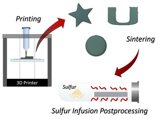
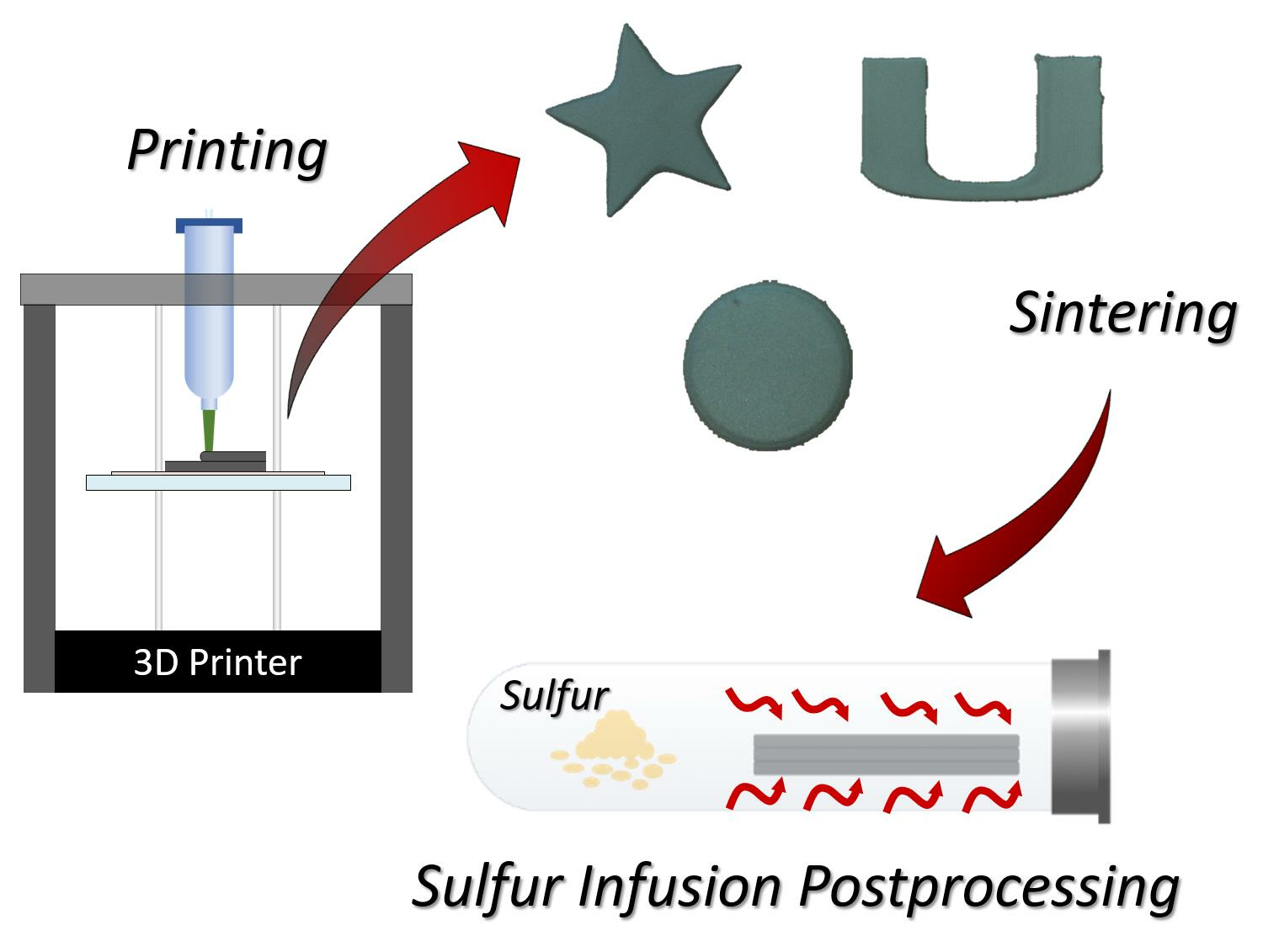
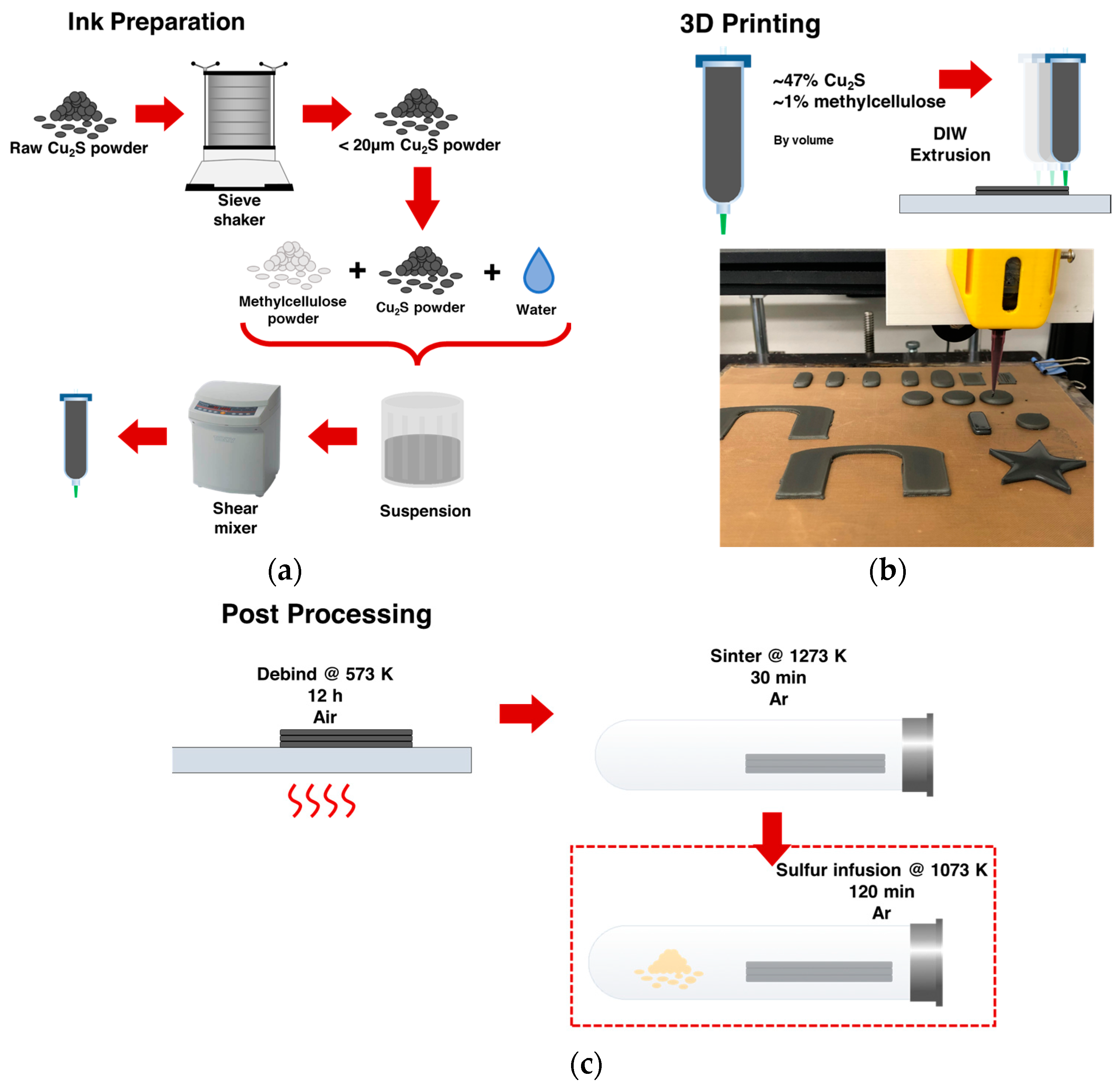
2.1. Ink Preparation and 3D Printing

Copper (I) sulfide powders (Cu2S) were purchased from American Elements (99.995% trace metals basis). Received powders were sieved using the Retsch AS 450 Control sieve shaker to obtain a size distribution of <20 μm and allow for maximum loading of the paste for direct ink writing. The material used for the paste was a mixture of water, methylcellulose (average MW ~200,000, The CandleMakers Store, East Liberty, OH, USA), and copper (I) sulfide powder. Methylcellulose and copper (I) sulfide powders were incrementally added to water and mixed at 1300 rpm for 2 min in a high-shear planetary mixer (Thinky ARE 310, Laguna Hills, CA, USA). This process was repeated until the mixture contained ~1% methylcellulose and ~47% copper (I) sulfide by volume, as shown in Figure 1a. The homogeneity of the ink was monitored visually after each mixing cycle. Once the consistency of the ink did not change after multiple mixes, it was determined that the particulates were fully exfoliated, and ink homogeneity was satisfied. After mixing, a 30-cc syringe was filled with thermoelectric paste, and an Ultimus V pressure regulator was used to extrude the material during the DIW process. An 840-μm tapered nozzle was used to print the paste at room temperature on a glass substrate lined with a Teflon sheet. The extrusion pressure was 15 psi while the print speed was maintained at 20 mms−1. Once the printing was completed, the printed structure was left in ambient air for 24 h to cure (Figure 1b).

2.2. Sintering and Sulfur Diffusion Post-Processing

3D printed specimens were placed in a muffle furnace at 573 K for 12 h in ambient air to remove the organic binder from the printed structures. This temperature and time were selected based on TGA experiments published in the literature [37] values for the decomposition of organic material and the porous nature of the sample aids in the decomposition as well. Sintering was then performed at 1273 K for 30 min under vacuum. Prior to the vacuum application, the heating chamber was purged with argon gas to minimize the oxygen content in the chamber. Due to the high sintering temperature, sulfur within the alloy volatilizes making the sample super-saturated with copper. Copper precipitates can be found within and on the surface of the sample after the sintering process is completed. This reduces the overall thermoelectric properties of the sample. To diffuse the lost sulfur back into the system and enhance the thermoelectric performance, the sintered specimens underwent a post-processing procedure where the samples were heated at 1073 K for 2 h with sulfur powder (99.5%, Alfa Aesar, Haverhill, MA, USA) in the vacuum sealed furnace and purged with argon gas, as shown in Figure 1c. The amount of sulfur powder used in post-processing was 5% of the total mass of the sample.

2.3. Characterization of Crystal Structure and Sulfur Content

Scanning electron microscopy (SEM) was conducted on sintered and post-processed samples. Images were taken on the Zeiss Gemini Field Emission SEM. Sputter coating commonly applied on SEM samples to minimize charging was not required due to the highly conductive nature of the samples. X-ray diffraction analysis (XRD) was performed on the Rigaku Smart Lab to characterize the crystal structure of the three sets of samples: (1) as supplied powder; (2) samples after sintering; and (3) samples after sintering and sulfur diffusion post-processing. In addition to XRD analysis to evaluate the effect of sulfur diffusion post-processing on the alloy morphology, sulfur content was also quantified using the LECO CS844 elemental analyzer following the methodology provided by the manufacturer. The device was calibrated prior to testing using 502–085 zinc sulfide reference material supplied by LECO.

2.4. Thermoelectric Characterization

Electrical conductivity and Seebeck coefficient of the 3D printed specimens were measured using the Linseis LSR-3 system. Electrical conductivity was calculated using the measured resistivity of the sample via the four-point probe method where a constant current was applied through the upper and lower electrodes and the voltage drop was recorded in the middle of the sample between two thermocouples. Simultaneously, the Seebeck coefficient measurement was conducted using an upper and lower thermal gradient of 30 K which was maintained using gradient heaters. The voltage and temperature differential were probed and recorded in the middle of the sample approximately 3 mm apart using the same platinum-coated thermocouples. All measurements were performed from room temperature to 774 K in a helium (He) environment, as shown in Figure S2.
Thermal conductivity ( κ ) of the 3D printed thermoelectric materials was calculated according to the following equation:
κ = D·Cp·ρ
where D is thermal diffusivity, Cp is specific heat, and ρ is the mass density. Prior to the thermal diffusivity measurements, samples were cut to 10 mm OD × 2 mm thickness and were sanded to achieve parallel contact surfaces. Sample dimensions were measured with a micrometer with ±1 μm accuracy. Thermal diffusivity (D) was performed on a Netzsch LFA 427 unit (Selb, Germany) using a 10 mm graphite holder in 100 K increments up to 774 K under the helium flow of 150 mL/min. The laser was operated at 700 V with a 0.5 ms pulse width and collected in an Indium antimonide (InSb) cryogenically cooled detector. The standard model with a linear background was used to fit the data to calculate the half–time. A Netzsch DSC 404 unit (Selb, Germany) was used to calculate the Cp of the samples up to 774 K using the Cp ratio method with sapphire as the standard at 50 mLmin−1 flow and Ar heated at 5 Kmin−1 in a platinum crucible. The sensitivity was calibrated against metal melting in platinum crucibles with an alumina liner. A constant value of 30 ppm-K−1 was used for the CTE from room temperature to 774 K for all samples. Thermal diffusivity and specific heat measurements are given in the Supplementary Figure S3. Densities (ρ) of the 3D printed parts were calculated using their geometrical dimensions and mass at room temperature and assumed to be unchanged as a function of temperature for the thermal conductivity calculations.

3. Results and Discussion

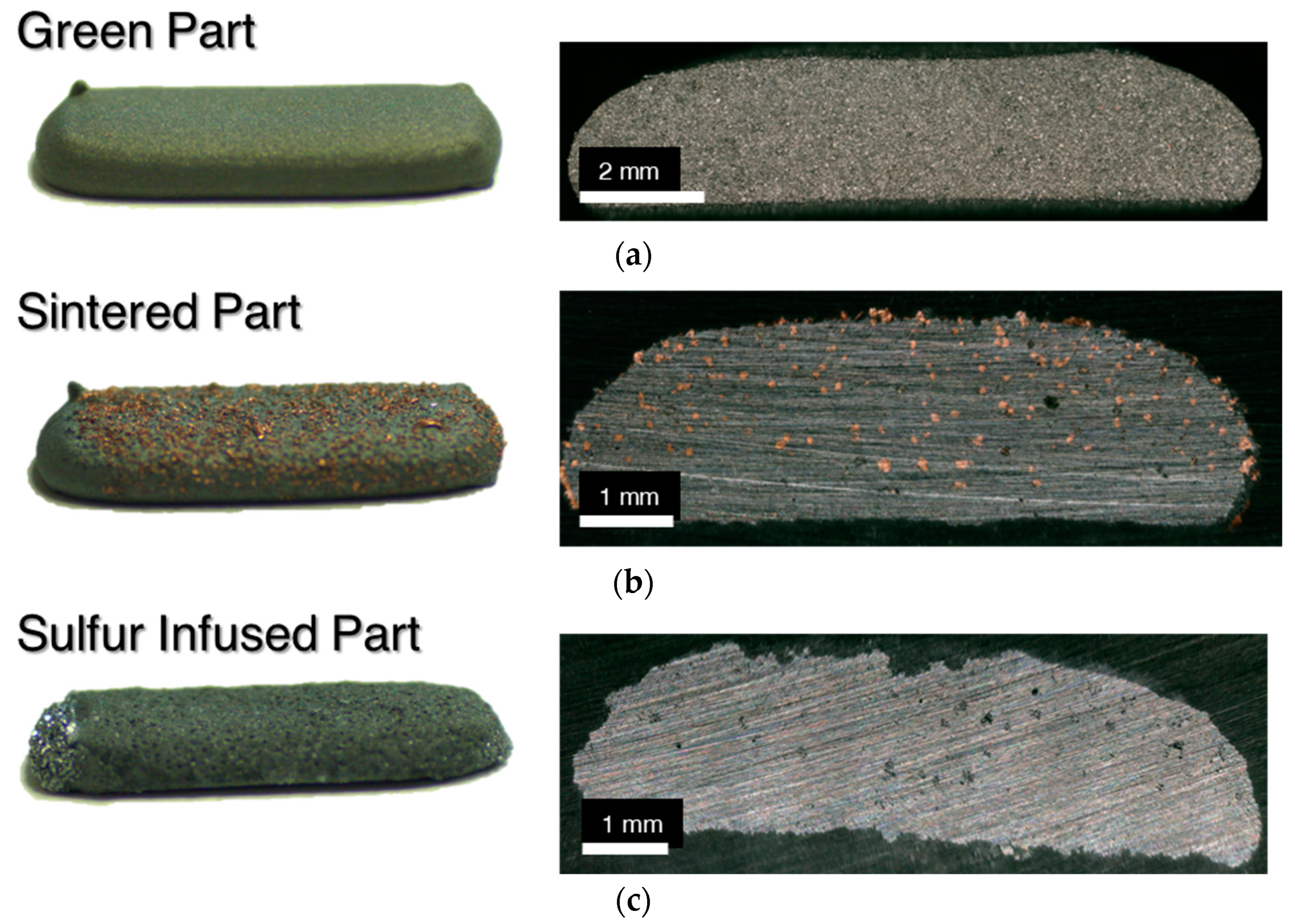
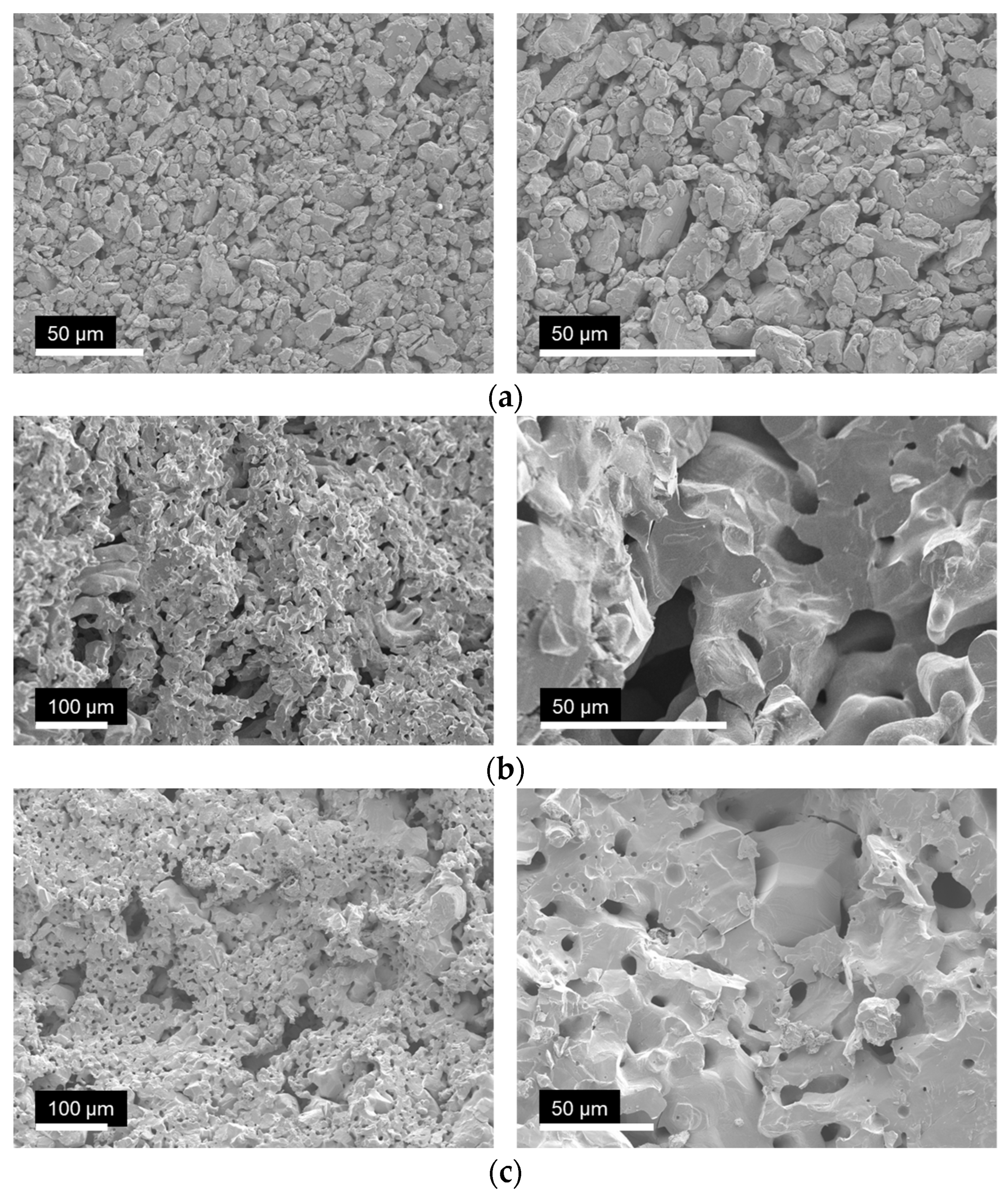
3.1. Structural and Morphological Analysis

Using the DIW technique, various complex geometry could be fabricated which would be extremely difficult and/or costly to achieve via traditional manufacturing. As shown in Figure 2, shape conformality for thermoelectric legs becomes feasible paving the way for unconventional TEG designs, such as annular or uni-leg form factors. Lattice structures (Figure 2b) were also fabricated demonstrating the enhanced design freedom of the direct ink writing process compared to the conventional manufacturing technologies.
Optical microscope images were taken of the 3D printed samples to observe the change in microstructure. Air cured samples were imaged as-is due to the delicate nature of the specimens. Sintered and sulfur-infused samples were encased using a hot mounting press in clear acrylic and polished for cross-sectional analysis. As shown in Figure 3b, after sintering, the copper precipitates from the solid solution within and on the surface of the sample due to the volatilization of sulfur. After the reintroduction of sulfur, some copper particles remain but they are greatly reduced in size as the precipitates are reabsorbed in the copper (I) sulfide solid solution (Figure 3c).
SEM imaging was conducted on the copper (I) sulfide samples at various stages of the manufacturing process. As shown in Figure 4a,b, the powder granules are clearly visible as individual entities in the samples after 3D printing and curing for 24 h at room temperature. The structural integrity of the printed specimens was achieved by simply using methylcellulose powder and water which keeps the Cu2S particles together in these samples. These samples prior to the sintering step are referred to as green parts.
The sintering temperature was chosen to be 1273 K which was 90% of the melting temperature of Cu2S [20]. Sintering time was optimized in systematic experimentation studies and 30 min was selected to maximize form retention of the samples (i.e., the tendency of the samples to warp or deform during sintering) and thermoelectric performance. It is hypothesized that the selection of too high of a sintering temperature would lead to loss of the original printed form factor along with an increase in thermal conductivity due to decreased phonon scattering; thus, decreasing overall TE performance. Similarly, too low of a sintering temperature would result in insufficient melting, and therefore powder granules would not properly coalesce to form mechanically solid samples. This would also decrease the electrical conductivity as an interconnected network is not properly formed within the samples. During the de-binding process performed at 573 K, the binding agent decomposes leaving a large amount of porosity, as shown in Figure 4b,c. The pores are generally uniform with a size of nearly 10 μm in diameter. Sintering also results in partial melting and coalescing of the individual Cu2S granules enhancing the structural integrity and TE properties of the fabricated specimens. Sulfur infusion post-processing performed on the sintered specimens does not lead to any notable morphological changes, as shown in Figure 4.
Densities of the green, sintered, and post-processed specimens are given in Table 1 [38]. During the thermal de-binding process, the binding agent (methylcellulose and water) is volatilized leaving behind pores in the sample. Between the thermal de-binding and sintering process, samples uniformly shrunk by 19.01% ± 4.71%. Compression testing was performed on an Instron 5564 universal test setup (1 kN load cell) using a testing strain rate of 0.5 mm/min parallel to the build direction. The data are shown in Figure 5. The compressive strength was evaluated at 15% strain resulting in a compressive strength of 8.3 MPa, 21.7 MPa, and 33.7 MPa for as-printed, sintered, and post-processed samples, respectively. This is comparable to bulk values in the literature for commercially used Bi0.5Sb1.5Te3, commonly found in TE modules [39].

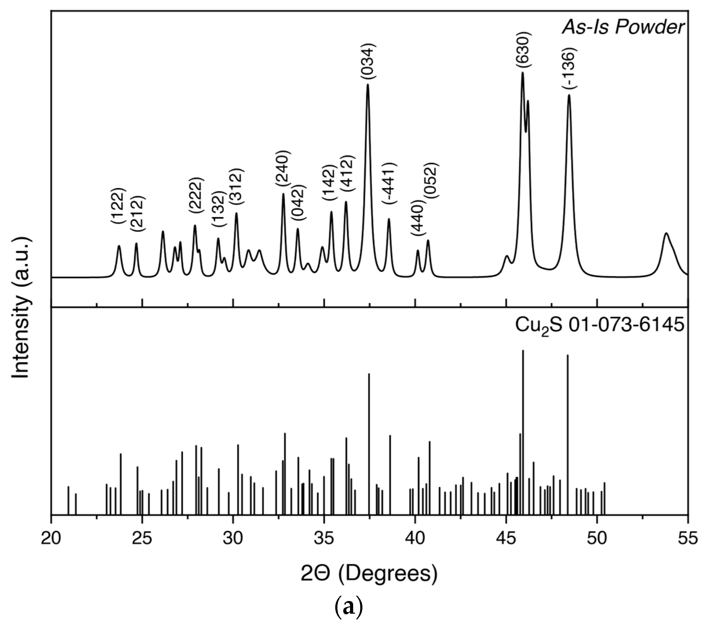
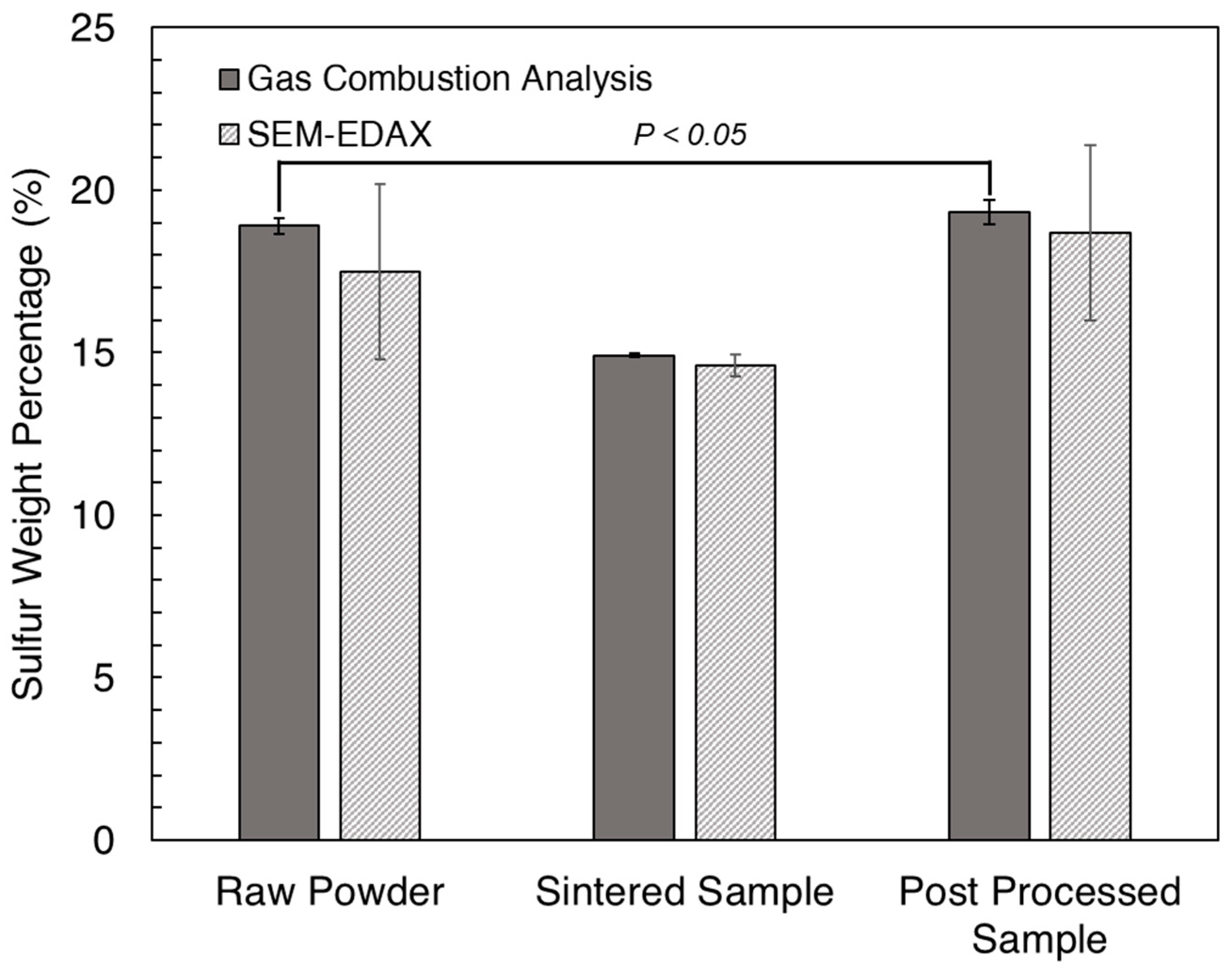
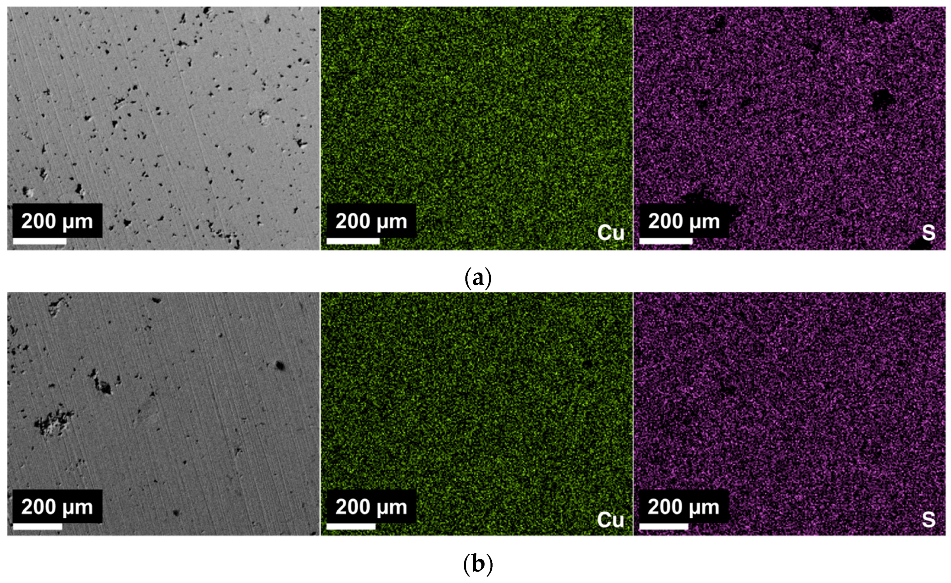
3.2. Compositional Analysis

Powder XRD was performed on (as-received powder) and on 3D printed parts (after sintering and after the sulfur infusion process) to observe the alterations in the chemical structure of Cu2-xS specimens in the sintering and post-processing steps. Prior to the XRD analysis, 3D printed samples were ground into a homogenous powder using a mortar and pestle. The XRD pattern data for the Cu2S powder, as received from the manufacturer, is shown in Figure 6a. According to these results, the precursor material was in close agreement with monoclinic Cu2S (ICDD 01-073-6145) which was expected to have minimal impurities present. Figure 6b presents the pattern data for Cu2-xS samples after sintering at 1273 K for 30 min. Strong Cu peaks are observed since sulfur volatilizes during the sintering process, allowing for the migration of free copper ions to the surface of the samples. The same phenomenon has been reported to occur in the literature [40]. However, after the sulfur infusion process, the Cu peaks are no longer as prominent as shown in Figure 6c, indicating the reabsorption of the free Cu into the material.
Figure 7 further supports the conclusions drawn in XRD results where the compositional weight percentages of sulfur in the samples were measured by the LECO CS844 analyzer and SEM-EDAX. As shown in this figure, as-received powder has a weight percentage of 18.89% ± 0.24% which is expected for stoichiometric Cu2S. There is a significant decrease in sulfur content to the weight percentage of 14.91% ± 0.05% after sintering was conducted at 1273 K. At this sintering temperature, sulfur may volatilize creating a copper excess mixture within the sample. After the sulfur infusion post-processing was performed, the sulfur weight percentage was elevated to 19.33% ± 0.36% effectively making the sample sulfur-rich. The difference in sulfur composition between the raw powder and post-processed sample is statistically significant (p-value < 0.05), evidencing that the sulfur-rich alloy was produced after the sulfur-infusion process was performed. To ensure a homogenous solid solution was fabricated x-ray mapping using scanning electron microscopy of the elemental distribution was performed, as shown in Figure 8. The bottom row represents the post-processed samples and shows that the distribution between Cu and S is homogeneous over the area pictured compared to the top row, where Cu precipitates are clearly visible in the sintered samples when comparing Figure 8a,b. The two images below show no sign of Cu precipitates.

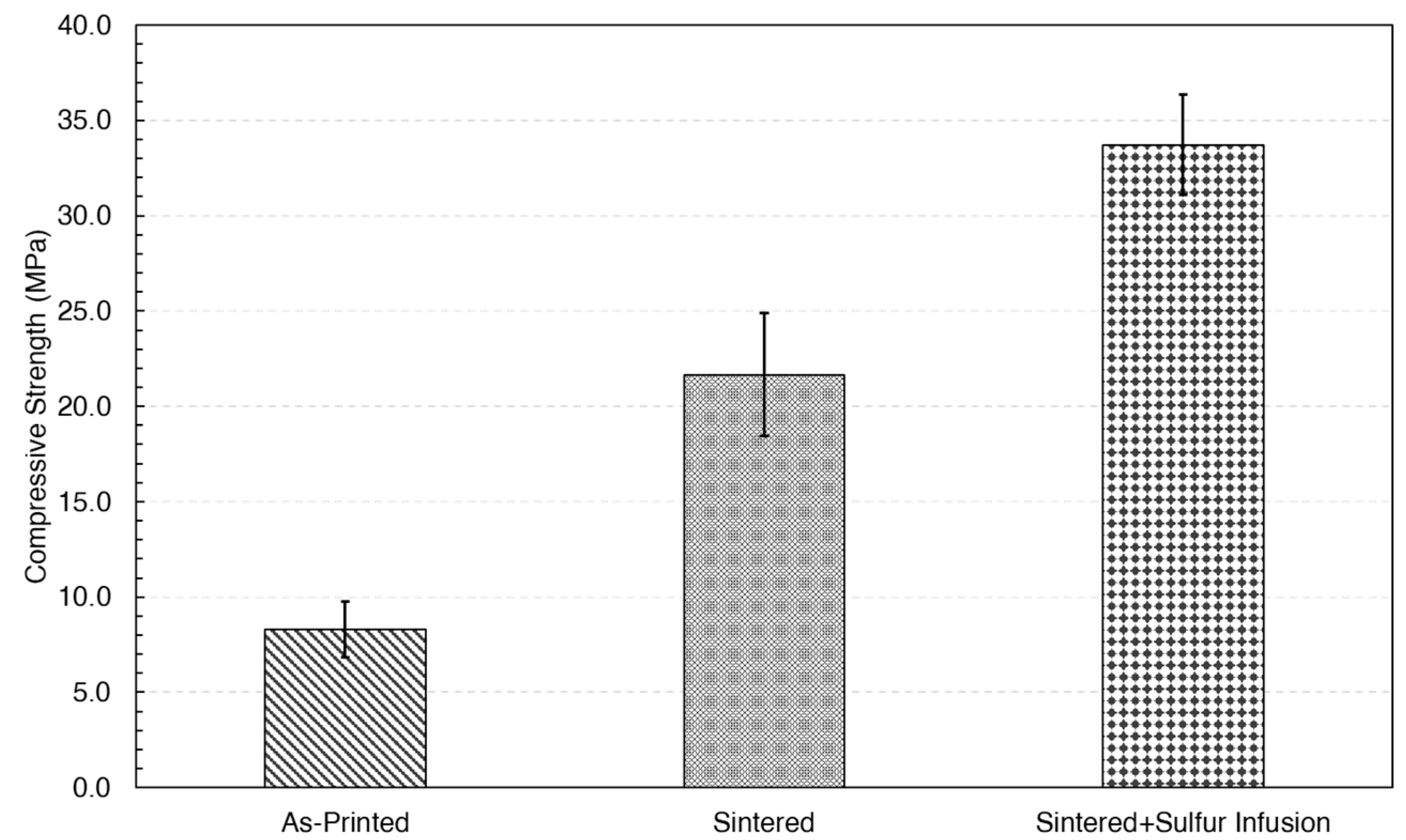
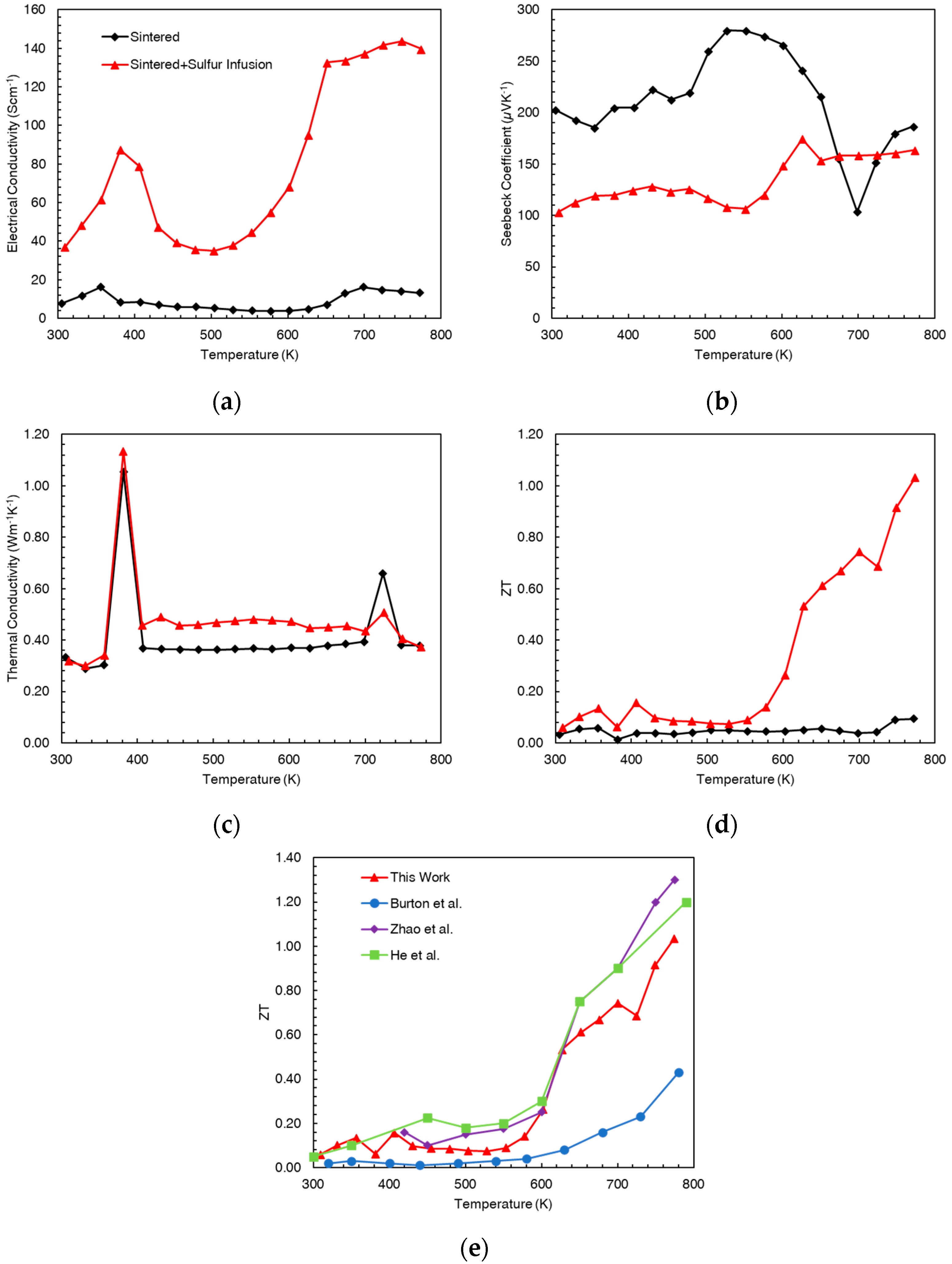
3.3. Thermoelectric Characterization

Figure 9 displays the electrical conductivity (σ), Seebeck coefficient (S), thermal conductivity (κ), and figure of merit (ZT) of sintered and sulfur-infused (post-processed) Cu2-xS samples in the temperature range from 300 to 800 K. For only sintered samples, the electrical conductivity ranged from 3 to 16 S-cm−1 (Figure 9a). However, for sulfur-infused specimens, there was a significant increase in electrical conductivity ranging from 35 to 143 S-cm−1. This can be attributed to the change in the material composition during the sulfur infusion process, as explained in the previous section. As reported previously by Sorokin [41], copper-rich Cu2-xS has very low electrical conductivity compared to sulfur-rich Cu2-xS. The slight difference in the Cu/S ratio can present large variations in electrical conductivity due to differences in mobility. The effect of transitioning from copper-rich to sulfur-rich material can be so dramatic that the electrical conductivity increases four orders of magnitude, as reported in this study. The variation of the Seebeck coefficient as a function of temperature is given in Figure 9b where higher Seebeck coefficients were reported for copper-rich (sintered) specimens compared to the sulfur-infused samples. The trend in the Seebeck coefficient versus sulfur deficiency is the inverse of that seen in electrical conductivity. This is due to the fact that the Seebeck coefficient is inversely correlated to carrier concentration, while electrical conductivity is directly correlated, as reported previously [42]. Sintered samples had S values ranging from 103 to 280 µV-K−1 while post-processed samples ranged from 103 to 175 µV-K−1. As the Cu/S ratio increases (observed in only sintered samples), the samples tend to behave more insulator-like with a higher Seebeck coefficient and a lower electrical conductivity [17].
To assess the effect of material stability at elevated temperature test conditions, the thermoelectric characterization cycle was repeated three times. Subsequent testing of the samples indicated slightly degraded performance after each cycle (Figure S1) with a decrease in electrical conductivity and an increase in the Seebeck coefficient. This can be attributed to the gradual loss of sulfur during the high-temperature segment of the testing cycle. Thermal conductivity results are given in Figure 9c. The thermal conductivities of both sintered and sulfur-infused samples are in the range from 0.4 to 0.7 W-m−1K−1. Post-processed specimens mark a slightly higher thermal conductivity level than the sintered samples level. The rapid jumps in the thermal conductivity plot are propagations from the specific heat data and these are most likely due to phase changes observed at those temperature points. Compared to the literature results for fully dense samples (κ ~0.3–0.6 W-m−1K−1 @ RT) [43], the values recorded here follow the same trend as expected. The average pore area was ~106 µm2 (Figure S4) which is beneficial in increasing the overall figure of merit.
When comparing the ZT results of the sintered and post-processed specimens, sulfur infusion significantly enhances the figure of merit (Figure 9d). For the sulfur infusion post-processed samples, a peak ZT value of 1.0 was observed at 780 K. This is the highest figure of merit value ever reported for a 3D printed copper (I) sulfide material at this temperature. The figure of merit results presented in Figure 9d distinctly shows the three-phase transformation zones. From room temperature to around ~370 K, copper (I) sulfide exhibits a monoclinic structure [44] characterized by high electrical conductivity. In the 370–700 K temperature range, samples have a hexagonal crystal structure [45] where copper (I) sulfide is the least efficient. In the temperature range above 700K, there is a phase transition from hexagonal to cubic Cu2-xS which has the most desirable properties in terms of thermoelectric performance and stability.

4. Conclusions

This study reports on the use of DIW 3D printing technology to fabricate Cu2-xS samples with high conversion efficiency by introducing the novel sulfur infusion post-processing method. Printed Cu2-xS samples were air cured and then subjected to high-temperature sintering at 1273 K where sulfur is lost to the environment creating a copper-rich alloy and resulting in poor thermoelectric performance. The sulfur infusion process reintroduces the lost sulfur allowing for the reabsorption of the precipitated copper and bringing the Cu/S ratio close to that of the stoichiometric copper (I) sulfide. Reverting the lost sulfur back to the sample significantly enhances the thermoelectric performance of the 3D printed materials. Printed and post-processed Cu2-xS marks electrical conductivity peaking at 143 S-cm−1 at 750 K, Seebeck coefficient of 175 µV-K−1 at 627 K, and thermal conductivity of nearly 0.5 W-m−1K−1. The culmination of these parameters results in a ZT value of 1.0 at 780 K which is the highest value ever reported for a 3D printed copper (I) sulfide thermoelectric at this temperature.
This work has demonstrated that the loss of sulfur is the key mechanism impairing the thermoelectric properties of additively manufactured Cu2-xS materials. The impaired properties can be reverted to the well-being state by introducing the lost sulfur into the material through an additional post-processing step. ZT was observed to increase nearly five (10) times as a result of the sulfur infusion process. Investigating the sulfur loss on thermoelectric properties of additively manufactured Cu2-xS and introducing a novel remedy for the impaired properties have the potential to greatly impact the thermoelectric industry since they pave the way for the fabrication of environment-friendly, earth-abundant Cu2-xS thermoelectrics with high conversion efficiency and high dimensional freedom.

Supplementary Materials

The following supporting information can be downloaded at: https://www.mdpi.com/article/10.3390/machines11090881/s1. Figure S1: Thermoelectric properties of sulfur-infused 3D printed Cu2-xS samples: (a) electrical conductivity; (b) Seebeck coefficient; and (c) figure of merit. Figure S2: Heating profile used for thermoelectric characterization with the Linseis LSR-3 system. Figure S3: Thermal diffusivity (a) and specific heat of (b) DIW Cu2-xS samples. Figure S4. Pore analysis was conducted using ImageJ analysis software. (a) Raw SEM image of cross-sectional area. (b) Areas of interest (i.e., pores/voids) are shown highlighted in red according to a user defined threshold to segment the image. (c) AOIs are then outlined and numbered. (d) Graphical display of the distribution of area pore size in µm2 calculated from the set of ten (10) images. Scale bars, 100 µm.

Author Contributions

Conceptualization, R.G., W.J.W., G.L.D.B., D.S., S.S. and E.C.; methodology, R.G. and J.W.D.; investigation, R.G., W.J.W. and J.W.D.; writing—original draft preparation, R.G.; writing—review and editing, G.L.D.B. and E.C.; supervision, E.C.; funding acquisition, D.S. All authors have read and agreed to the published version of the manuscript.

Funding

This work was funded by the U.S. Army Combat Capabilities Development Command Armaments Center under project number DOTC-19-01-INIT0903.

Data Availability Statement

The raw/processed data required to reproduce these findings cannot be shared at this time due to technical or time limitations. All raw data will be made publicly available before the publication of the manuscript.

Conflicts of Interest

The authors declare no conflict of interest.

References

  1. Twaha, S.; Zhu, J.; Yan, Y.; Li, B. A comprehensive review of thermoelectric technology: Materials, applications, modelling and performance improvement. Renew. Sustain. Energy Rev. 2016, 65, 698–726. [Google Scholar] [CrossRef]
  2. Pourkiaei, S.M.; Ahmadi, M.H.; Sadeghzadeh, M.; Moosavi, S.; Pourfayaz, F.; Chen, L.; Pour Yazdi, M.A.; Kumar, R. Thermoelectric cooler and thermoelectric generator devices: A review of present and potential applications, modeling and materials. Energy 2019, 186, 115849. [Google Scholar] [CrossRef]
  3. Goldsmid, H.J. Bismuth Telluride and Its Alloys as Materials for Thermoelectric Generation. Materials 2014, 7, 2577–2592. [Google Scholar] [CrossRef]
  4. Poudel, B.; Hao, Q.; Ma, Y.; Lan, Y.C.; Minnich, A.; Yu, B.; Yan, X.A.; Wang, D.Z.; Muto, A.; Vashaee, D.; et al. High-thermoelectric performance of nanostructured bismuth antimony telluride bulk alloys. Science 2008, 320, 634–638. [Google Scholar] [CrossRef]
  5. Witting, I.T.; Chasapis, T.C.; Ricci, F.; Peters, M.; Heinz, N.A.; Hautier, G.; Snyder, G.J. The Thermoelectric Properties of Bismuth Telluride. Adv. Electron. Mater. 2019, 5, 1800904. [Google Scholar] [CrossRef]
  6. Yamashita, O.; Tomiyoshi, S.; Makita, K. Bismuth telluride compounds with high thermoelectric figures of merit. J. Appl. Phys. 2003, 93, 368–374. [Google Scholar] [CrossRef]
  7. Zhang, H.; Hobbis, D.; Nolas, G.S.; LeBlanc, S. Laser additive manufacturing of powdered bismuth telluride. J. Mater. Res. 2018, 33, 4031–4039. [Google Scholar] [CrossRef]
  8. Dughaish, Z.H. Lead telluride as a thermoelectric material for thermoelectric power generation. Phys. B 2002, 322, 205–223. [Google Scholar] [CrossRef]
  9. LaLonde, A.D.; Pei, Y.Z.; Wang, H.; Snyder, G.J. Lead telluride alloy thermoelectrics. Mater. Today 2011, 14, 526–532. [Google Scholar] [CrossRef]
  10. Pei, Y.Z.; Heinz, N.A.; LaLonde, A.; Snyder, G.J. Combination of large nanostructures and complex band structure for high performance thermoelectric lead telluride. Energy Environ. Sci. 2011, 4, 3640–3645. [Google Scholar] [CrossRef]
  11. Liu, H.; Shi, X.; Xu, F.; Zhang, L.; Zhang, W.; Chen, L.; Li, Q.; Uher, C.; Day, T.; Snyder, G.J. Copper ion liquid-like thermoelectrics. Nat. Mater. 2012, 11, 422–425. [Google Scholar] [CrossRef] [PubMed]
  12. Mulla, R.; Rabinal, M.H.K. Copper Sulfides: Earth-Abundant and Low-Cost Thermoelectric Materials. Energy Technol. 2019, 7, 1800850. [Google Scholar] [CrossRef]
  13. Oztan, C.Y.; Hamawandi, B.; Zhou, Y.; Ballikaya, S.; Toprak, M.S.; Leblanc, R.M.; Coverstone, V.; Celik, E. Thermoelectric performance of Cu2Se doped with rapidly synthesized gel-like carbon dots. J. Alloys Compd. 2021, 864, 157916. [Google Scholar] [CrossRef]
  14. Kang, S.D.; Pöhls, J.-H.; Aydemir, U.; Qiu, P.; Stoumpos, C.C.; Hanus, R.; White, M.A.; Shi, X.; Chen, L.; Kanatzidis, M.G.; et al. Enhanced stability and thermoelectric figure-of-merit in copper selenide by lithium doping. Mater. Today Phys. 2017, 1, 7–13. [Google Scholar] [CrossRef]
  15. Shi, D.-l.; Geng, Z.-m.; Shi, L.; Li, Y.; Lam, K.-h. Thermal stability study of Cu1.97Se superionic thermoelectric materials. J. Mater. Chem. C 2020, 8, 10221–10228. [Google Scholar] [CrossRef]
  16. Liu, W.D.; Yang, L.; Chen, Z.G.; Zou, J. Promising and Eco-Friendly Cu2X-Based Thermoelectric Materials: Progress and Applications. Adv. Mater. 2020, 32, e1905703. [Google Scholar] [CrossRef]
  17. Okamoto, K.; Kawai, S. Electrical Conduction and Phase Transition of Copper Sulfides. Jpn. J. Appl. Phys. 1973, 12, 1130. [Google Scholar] [CrossRef]
  18. Nieroda, P.; Leszczyński, J.; Mikuła, A.; Mars, K.; Kruszewski, M.J.; Koleżyński, A. Thermoelectric properties of Cu2S obtained by high temperature synthesis and sintered by IHP method. Ceram. Int. 2020, 46, 25460–25466. [Google Scholar] [CrossRef]
  19. Zhao, L.; Wang, X.; Fei, F.Y.; Wang, J.; Cheng, Z.; Dou, S.; Wang, J.; Snyder, G.J. High thermoelectric and mechanical performance in highly dense Cu2−xS bulks prepared by a melt-solidification technique. J. Mater. Chem. A 2015, 3, 9432–9437. [Google Scholar] [CrossRef]
  20. Chakrabarti, D.J.; Laughlin, D.E. The Cu-S (Copper-Sulfur) system. Bull. Alloy Phase Diagr. 1983, 4, 254–271. [Google Scholar] [CrossRef]
  21. He, Y.; Day, T.; Zhang, T.; Liu, H.; Shi, X.; Chen, L.; Snyder, G.J. High thermoelectric performance in non-toxic earth-abundant copper sulfide. Adv. Mater. 2014, 26, 3974–3978. [Google Scholar] [CrossRef] [PubMed]
  22. Dennler, G.; Chmielowski, R.; Jacob, S.; Capet, F.; Roussel, P.; Zastrow, S.; Nielsch, K.; Opahle, I.; Madsen, G.K.H. Are Binary Copper Sulfides/Selenides Really New and Promising Thermoelectric Materials? Adv. Energy Mater. 2014, 4, 1301581. [Google Scholar] [CrossRef]
  23. Wei, T.-R.; Qin, Y.; Deng, T.; Song, Q.; Jiang, B.; Liu, R.; Qiu, P.; Shi, X.; Chen, L. Copper chalcogenide thermoelectric materials. Sci. China Mater. 2018, 62, 8–24. [Google Scholar] [CrossRef]
  24. Li, M.; Liu, Y.; Zhang, Y.; Han, X.; Zhang, T.; Zuo, Y.; Xie, C.; Xiao, K.; Arbiol, J.; Llorca, J.; et al. Effect of the Annealing Atmosphere on Crystal Phase and Thermoelectric Properties of Copper Sulfide. ACS Nano 2021, 15, 4967–4978. [Google Scholar] [CrossRef] [PubMed]
  25. Qiu, P.; Agne, M.T.; Liu, Y.; Zhu, Y.; Chen, H.; Mao, T.; Yang, J.; Zhang, W.; Haile, S.M.; Zeier, W.G.; et al. Suppression of atom motion and metal deposition in mixed ionic electronic conductors. Nat. Commun. 2018, 9, 2910. [Google Scholar] [CrossRef]
  26. Oztan, C.; Ballikaya, S.; Ozgun, U.; Karkkainen, R.; Celik, E. Additive manufacturing of thermoelectric materials via fused filament fabrication. Appl. Mater. Today 2019, 15, 77–82. [Google Scholar] [CrossRef]
  27. Burton, M.; Howells, G.; Atoyo, J.; Carnie, M. Printed Thermoelectrics. Adv. Mater. 2022, 34, e2108183. [Google Scholar] [CrossRef]
  28. Kim, F.; Yang, S.E.; Ju, H.; Choo, S.; Lee, J.; Kim, G.; Jung, S.H.; Kim, S.; Cha, C.; Kim, K.T.; et al. Direct ink writing of three-dimensional thermoelectric microarchitectures. Nat. Electron. 2021, 4, 579–587. [Google Scholar] [CrossRef]
  29. Jo, S.; Choo, S.; Kim, F.; Heo, S.H.; Son, J.S. Ink Processing for Thermoelectric Materials and Power-Generating Devices. Adv. Mater. 2019, 31, 1804930. [Google Scholar] [CrossRef]
  30. Kato, K.; Hagino, H.; Miyazaki, K. Fabrication of Bismuth Telluride Thermoelectric Films Containing Conductive Polymers Using a Printing Method. J. Electron. Mater. 2013, 42, 1313–1318. [Google Scholar] [CrossRef]
  31. Amin, A.; Huang, R.; Newbrook, D.; Sethi, V.; Yong, S.; Beeby, S.; Nandhakumar, I. Screen-printed bismuth telluride nanostructured composites for flexible thermoelectric applications. J. Phys.-Energy 2022, 4, 024003. [Google Scholar] [CrossRef]
  32. Chen, B.L.; Kruse, M.; Xu, B.; Tutika, R.; Zheng, W.; Bartlett, M.D.; Wu, Y.; Claussen, J.C. Flexible thermoelectric generators with inkjet-printed bismuth telluride nanowires and liquid metal contacts. Nanoscale 2019, 11, 5222–5230. [Google Scholar] [CrossRef]
  33. Kim, F.; Kwon, B.; Eom, Y.; Lee, J.E.; Park, S.; Jo, S.; Park, S.H.; Kim, B.S.; Im, H.J.; Lee, M.H.; et al. 3D printing of shape-conformable thermoelectric materials using all-inorganic Bi2Te3-based inks. Nat. Energy 2018, 3, 301–309. [Google Scholar] [CrossRef]
  34. Burton, M.R.; Mehraban, S.; McGettrick, J.; Watson, T.; Lavery, N.P.; Carnie, M.J. Earth abundant, non-toxic, 3D printed Cu2−xS with high thermoelectric figure of merit. J. Mater. Chem. A 2019, 7, 25586–25592. [Google Scholar] [CrossRef]
  35. Pan, S.-H.; Yao, G.-C.; Cui, Y.-N.; Meng, F.-S.; Luo, C.; Zheng, T.-Q.; Singh, G. Additive manufacturing of tungsten, tungsten-based alloys, and tungsten matrix composites. Tungsten 2022, 5, 1–31. [Google Scholar] [CrossRef]
  36. Caccia, M.; Tabandeh-Khorshid, M.; Itskos, G.; Strayer, A.R.; Caldwell, A.S.; Pidaparti, S.; Singnisai, S.; Rohskopf, A.D.; Schroeder, A.M.; Jarrahbashi, D.; et al. Ceramic–metal composites for heat exchangers in concentrated solar power plants. Nature 2018, 562, 406–409. [Google Scholar] [CrossRef]
  37. Zohuriaan, M.J.; Shokrolahi, F. Thermal studies on natural and modified gums. Polym. Test. 2004, 23, 575–579. [Google Scholar] [CrossRef]
  38. Ramdohr, P. The Ore Minerals and Their Intergrowths; Elsevier Science: Amsterdam, The Netherlands, 2013. [Google Scholar]
  39. Zheng, Y.; Xie, H.; Shu, S.; Yan, Y.; Li, H.; Tang, X. High-Temperature Mechanical and Thermoelectric Properties of p-Type Bi0.5Sb1.5Te3 Commercial Zone Melting Ingots. J. Electron. Mater. 2013, 43, 2017–2022. [Google Scholar] [CrossRef]
  40. Cook, W.R. Phase Changes in Cu2S as a Function of Temperature; National Bureau of Standards: Gaithersburg, MD, USA, 1972. [Google Scholar]
  41. Sorokin, G.P.; Paradenko, A.P. Electrical Properties of Cu2S. Sov. Phys. J. 1966, 9, 59–61. [Google Scholar] [CrossRef]
  42. Snyder, G.J.; Toberer, E.S. Complex thermoelectric materials. Nat. Mater. 2008, 7, 105–114. [Google Scholar] [CrossRef]
  43. Nieroda, P.; Ziewiec, K.; Leszczyński, J.; Rutkowski, P.; Koleżyński, A. Extremely Fast and Cheap Densification of Cu2S by Induction Melting Method. Materials 2021, 14, 7311. [Google Scholar] [CrossRef] [PubMed]
  44. Roseboom, E.H., Jr. An investigation of the system Cu-S and some natural copper sulfides between 25 and 700 C. Econ. Geol. 1966, 61, 641–672. [Google Scholar] [CrossRef]
  45. Posfai, M.; Buseck, P.R. Djurleite, digenite, and chalcocite: Intergrowths and transformations. Am. Mineral. 1994, 79, 308–315. [Google Scholar]
Figure 1. Schematic of the multi-step fabrication process applied to produce Cu2-xS samples: (a) ink preparation; (b) 3D printing; and (c) post-processing.
Machines 11 00881 g001
Figure 2. 3D geometries capable of being produced using DIW methodologies: (a) solid geometries and (b) lattice structures.
Machines 11 00881 g002
Figure 3. Direct ink writing (DIW) 3D printed samples (a) air cured, (b) sintered, and (c) post sulfur infusion process along with accompanying cross-section.
Machines 11 00881 g003
Figure 4. SEM of thermoelectric samples (a) after printing and room temperature curing, (b) after high-temperature sintering, and (c) after the sulfur infusion post-processing.
Machines 11 00881 g004
Figure 5. Compressive strength at various stages of DIW fabricated samples. Error bars represent standard deviation.
Machines 11 00881 g005
Figure 6. XRD data of (a) Cu2S as−is powder, (b) sintered sample, and (c) sintered + sulfur−infused sample.
Machines 11 00881 g006aMachines 11 00881 g006b
Figure 7. Variation of sulfur compositional at different stages of the fabrication process was measured using gas combustion and SEM-EDAX analysis. Error bars represent standard deviation (p-value was calculated using a one-tailed two-sample t-test. A difference between sample sets can be stated with confidence since the value is less than 0.05.).
Machines 11 00881 g007
Figure 8. SEM imaging of a randomly selected area, with respecting element mapping of Cu and S for (a) sintered samples and (b) post-processed samples.
Machines 11 00881 g008
Figure 9. Thermoelectric properties of 3D printed Cu2-xS samples: (a) electrical conductivity, (b) Seebeck coefficient, (c) thermal conductivity, and (d) figure of merit ZT; and (e) figure of merit compared to other values in the recorded literature [19,21,34].
Machines 11 00881 g009
Table 1. Volumetric density of copper (I) sulfide samples after printing, after sintering, and after the sulfur infusion process.
Sample IDDensity (g/cm3)Standard Error (SE)Relative Density
Printed Part2.790.0449.9
Sintered2.840.0350.8
Post-Processed2.680.0747.8
The literature value for bulk density of Cu2S: 5.6 g/cm3 [38].
Disclaimer/Publisher’s Note: The statements, opinions and data contained in all publications are solely those of the individual author(s) and contributor(s) and not of MDPI and/or the editor(s). MDPI and/or the editor(s) disclaim responsibility for any injury to people or property resulting from any ideas, methods, instructions or products referred to in the content.

