Article

A Novel Method for LCD Module Alignment and Particle Detection in Anisotropic Conductive Film Bonding

1
CAS Engineering Laboratory for Intelligent Industrial Vision, Institute of Automation, Chinese Academy of Sciences, Beijing 100190, China
2
The School of Artificial Intelligence, University of Chinese Academy of Sciences, Beijing 100049, China
3
CASI Vision Technology Co., Ltd., Luoyang 471000, China
*
Author to whom correspondence should be addressed.
Machines 2023, 11(1), 49; https://doi.org/10.3390/machines11010049
Submission received: 30 November 2022 / Revised: 27 December 2022 / Accepted: 28 December 2022 / Published: 1 January 2023
(This article belongs to the Special Issue Social Manufacturing on Industrial Internet)

Abstract

:
In this paper, we propose a misalignment correct method and a particle detection algorithm to improve the accuracy in the quality inspection of the LCD module after the anisotropic conductive film (ACF) bonding. We use only one camera to acquire images of multiple positions in order to establish the transformation from the image space to the world coordinate. Our method can accurately determine the center of rotation of the carrier table and calculate the deviation of position and angle of the tested module. Compared to traditional ways that rely on multiple cameras to align the large-sized product, our method has the advantages of simple structure, low cost, and fast calibration process. The particle detection is performed after positioning all bumps of the bonded module. The gray morphology-based algorithm is developed to detect the extreme point of every particle and refine the particle result through blob analysis. This method reduces the over-checking rate and performs better on the detection precision for dense particles. We verify the effectiveness of our proposed methods in our experiments. The alignment error can be less than 0.05 mm, and the accuracy of the particle detection is 93% while the recall rate is 92.4%.

1. Introduction

Liquid crystal display (LCD) panels have been widely used in smartphones, car monitors, and other industries. To fit the proliferated applications with different sizes and shapes, LCD modules are expected to be more integrated, thinner, and of higher resolution. Anisotropic conductive film (ACF) bonding technology, as the key process in the production of LCD modules, is extremely important in order to achieve a higher signal density and smaller overall package, which can enable the LCD modules more light-weighted and miniaturized. To reduce the size of the module, circuit components such as integrated circuits (ICs) and flexible printed circuits (FPCs) are expected to be connected to display panels at a higher level of integration.
ACF is an important material that serves as a connector to achieve such a level of integration. The authors of [1,2,3] examined the mechanical reliability of the ACF and considered it as a low-cost and reliable material that can be used in semiconductors packaging. As shown in 
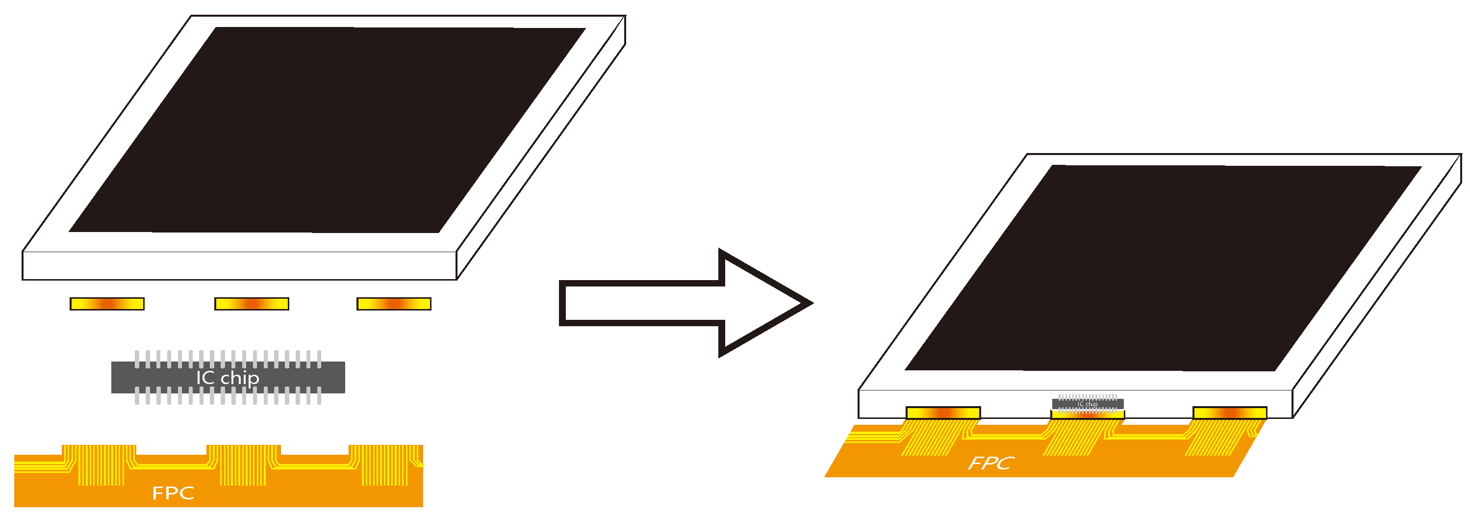
Figure 1, with the ACF, multiple components can be integrated into the display panel to form a compact LCD module. Such a material can achieve both a mechanical and electrical link between the substrates of peripheral circuits to that of the LCD.
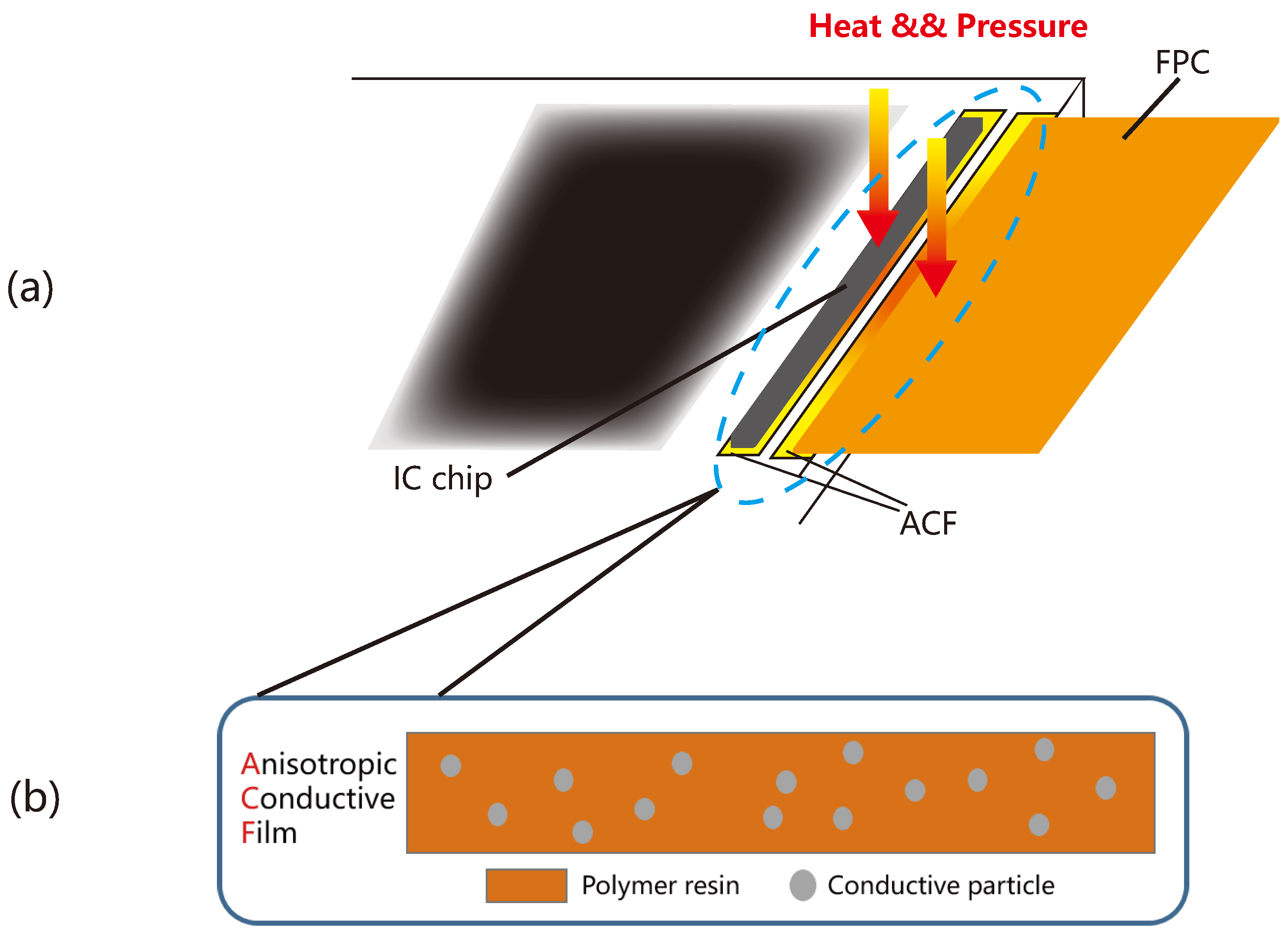
Figure 2a shows a detailed bonding process, in which the ACF is first attached to the panel substrates, and the substrates of ICs or FPCs can be further glued to it to realize a reliable connection between components. This process is called ACF bonding. As Figure 2b shows, the ACF mainly composes of conductive particles and polymer resin. The conductive particles provide the ability of conductivity, while the resin works as an adhesive to hold the LCD panel tightly with other circuits. ACF allows the two components, namely, the LCD panel and ICs or FPCs in our application, to create a reliable bond and enable electrical interconnection. Similar conducting polymer and metal nanoparticle ink have also been developed in [4,5] to fabricate materials with higher conductivity, thus improving the electrical performance of printed electronics. Mainly used processes include bonding integrated circuits (ICs) or flexible printed circuits (FPCs) onto the glass substrates, which are called chip-on-glass (COG) and flex-on-glass (FOG), respectively.
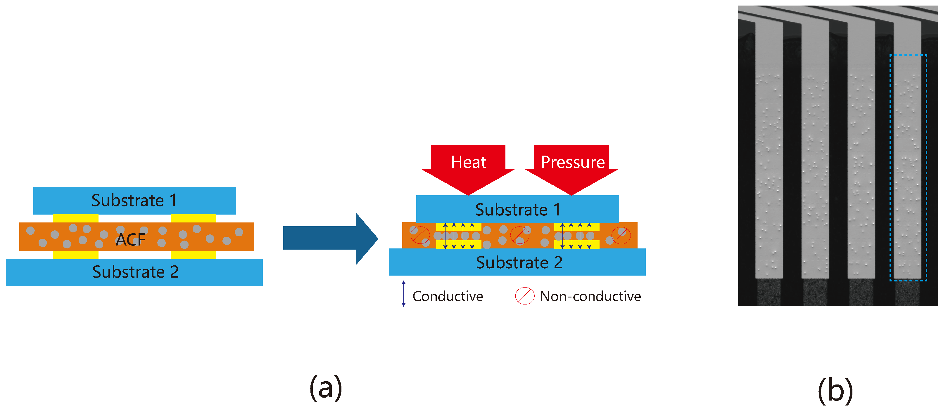
The conductivity of the ACF is explained in Figure 3a, where the ACF is sandwiched between the two substrates. After a period of heat and pressure, the indium tin oxide (ITO) bumps of the substrates are bonded closer, thus trapping some conductive particles. The interconnection is established by these trapped particles, and the power and signal can be transmitted from external components into the display module. After the ACF bonding process, the appearance of the bump areas taken by the camera is shown in Figure 3b. Conductive particles on the bump areas can be viewed from those taken images. As conductivity is a significant indicator of the quality of LCD modules, extensive studies have been conducted to investigate the factors that contribute to poor conductivity. The traditional method directly tests the resistance of the LCD module after the bonding process, which is time-consuming and may inflict damage to test modules. According to studies [6,7,8,9,10,11], the number and distribution of conductive particles are essential factors to the conductivity. Therefore, it has become a popular method for LCD manufacturing to verify the conductivity by calculating the number of conductive particles. However, the manual inspection method depends on sophisticated instruments to perform the detection, and due to the low efficiency of labor work, random sampling is usually used in the industry. Such a sampling method is less accurate, and with the mass production of LCD panels, inspection methods that rely on human labor cannot satisfy the growing manufacturing scale. Meanwhile, due to the small size of conductive particles, whose diameter is normally 3–5 μm, it is difficult to obtain high-resolution information about particles using human eyes or traditional instruments.
To improve the detection efficiency and accuracy without potential contact damage, the automated optical inspection (AOI), equipped with novel optical imaging methods and machine vision algorithms, has been developed by studies [12,13,14,15,16,17,18,19,20]. The AOI primarily uses the image sensor to acquire high-quality digital images of products and then draws upon a machine vision algorithm to identify the target objects in those images based on the features of the target. Many studies attempt to align the object module to the fiducial position to ensure a consistent imaging condition thus helping improve the detection result. For a large module, multiple cameras-based methods [21,22,23,24] are preferred because of higher precision. However, such methods usually repeatedly calculated the offset to reduce the alignment error, for example, an iterative algorithm proposed in [21]. Moreover, studies including [22,24] required multiple shots and movements for alignment, and they assumed a fixed center of rotation of the platform, which cannot be applied to other applications when the module sizes change. The utilization of a specialized marker and alignment layers were employed by the author of [25] in order to achieve precise positioning of the microlens within the array. In our proposed misalignment correction method, one single camera is used to take images of the feature mark on the both ends of the LCD module. This method can enhance the accuracy of alignment while reducing the alignment time by determining the center of rotation and calculating the displacement of the tested module in one stage.
It remains challenging to accurately and quickly detect the number of particles on the small bumps relative to a large entire image of the LCD module. The author of [13] combined differential interference contrast (DIC) prism with the CCD camera and achieved effective and high-contrast imaging of particles. The particles in the image represented spheres composing a bright part and a dark part. The author of [12] improved the Prewitt mask to calculate the image gradient and extract the extreme points using Otsu thresholding. Another study [26] also took the gray distribution of the particles as the feature to separate the original image into a light and a dark part. They then selected the more informative part by comparing the image entropy of the two parts. After clustering gray values in the selected image part, the center regions of particles were determined by the first two values in clusters. However, the aforementioned methods perform poorly in detecting particles when imaging illumination is weak or the particles are heavily overlapped. The gradient-based method is sensitive to the gradient change which makes it easy to recognize more particles than are actually there, especially along edge areas of the image. The clustering-based method has an unstable result in varying illumination conditions and leads to a low detection rate compared to the total number of particles to be checked. In this paper, we also propose a novel particle detection algorithm to improve the detection accuracy of the ACF task. This algorithm emphasizes the region of each particle based on the gray dilation morphology and then restores all particles by finding the extreme points of particles. The main contributions of this article are listed below.
(1)
A novel misalignment correction method is proposed to determine the transition and rotation of the carrier table to ensure a consistent imaging area, which can be achieved by taking twelve images in one iteration. The requirement for assembly accuracy of the alignment module is reduced through the proposed method.
(2)
A robust and fast detection algorithm is presented for checking the number of conductive particles.
(3)
A complete AOI system is constructed to meet the demand for in-line process inspection, which can perform miscellaneous tasks including alignment calibration and correction and particle detection.
This paper is organized as follows. In Section 2, the system design is presented, followed by the misalignment correction method and particle detection algorithm. Details of the experiment results are provided in Section 3. Finally, a conclusion and limitation of the current work are given in Section 4.

2. Materials and Methods

2.1. Automatic Inspection System

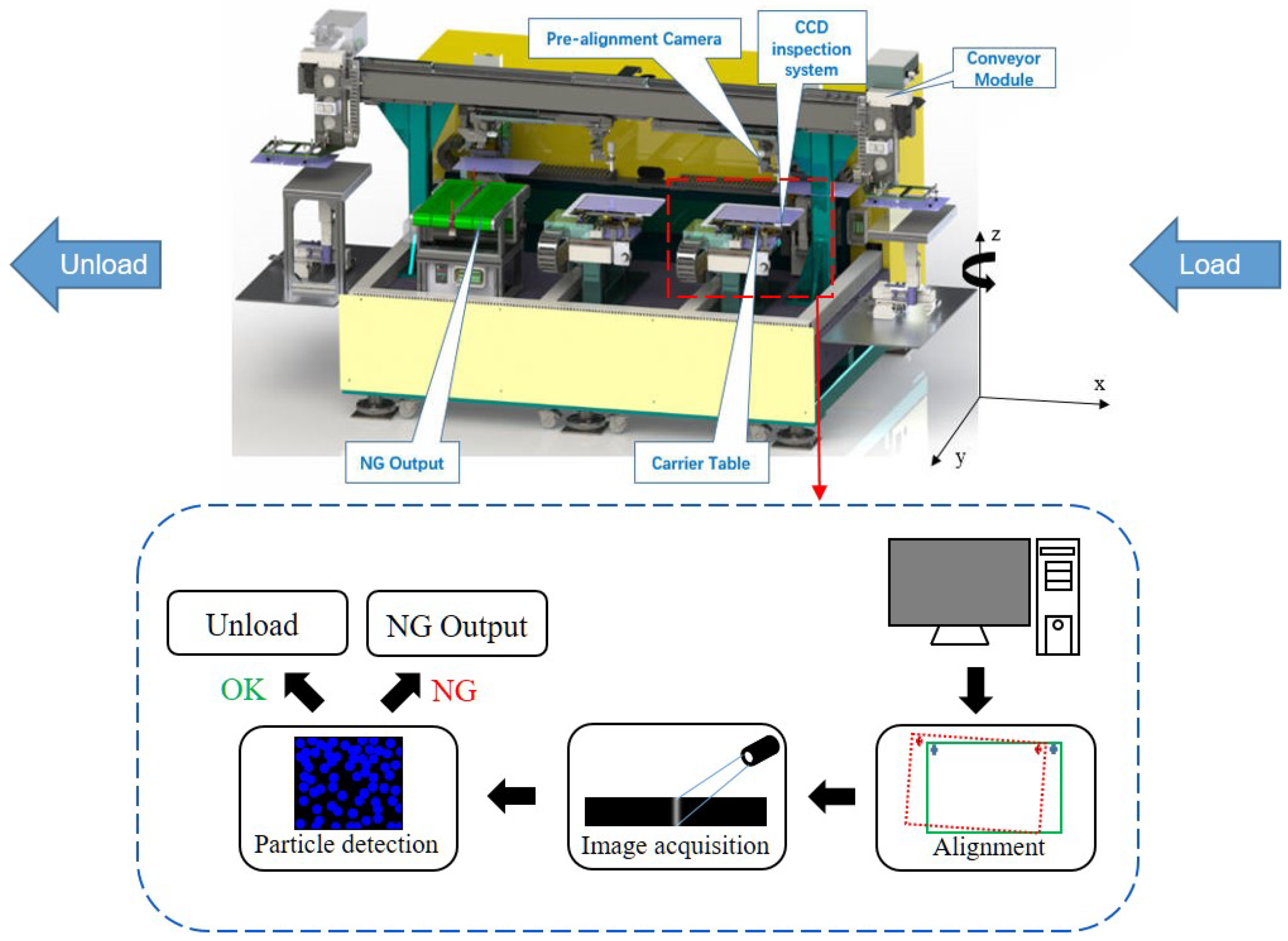
The architecture and major modules of the inspection system are shown in Figure 4. Table 1 lists the parameters and manufacturers of the main modules of the automatic inspection system. The loading and unloading modules are placed at both ends to connect with an existing assembly line. Specifically, the load unit receives LCD modules from the upstream line after they complete the bonding process, while non-defective products can be conveyed to the next stage through unload unit. As shown in 
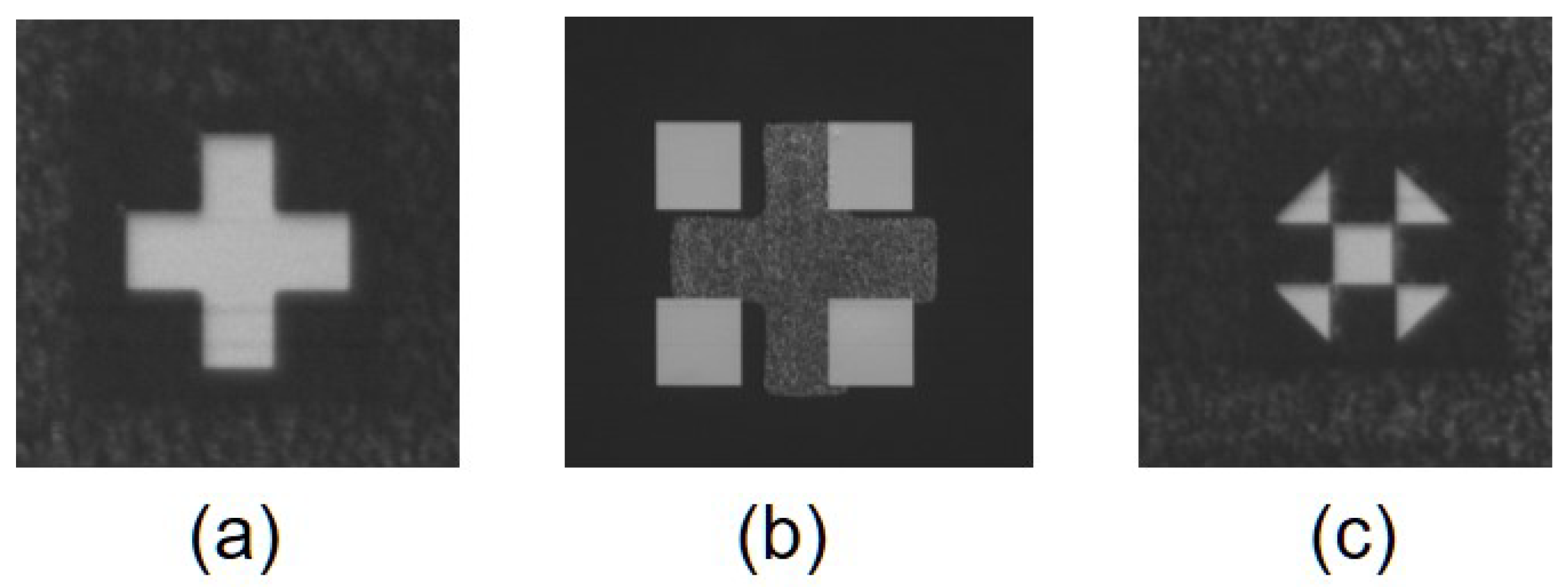
Figure 4, the system mainly includes five core modules. The conveyor module contains a robotic gripper equipped with a suction cup to softly attach the detected material from upstream and then lay it on the carrier table. The pre-alignment camera is then triggered to acquire the image of the LCD module at both ends of the corner, where we search the mark pattern as the feature point for calibration and alignment calculation afterward. As shown in Figure 5, the mark pattern is a special shape usually printed on the circuit board of the module and can be used as a feature point because of its distinctiveness. The carrier table can be controlled to translate and rotate according to the result of misalignment correction. After the alignment process, the CCD camera is initiated to scan the LCD module and acquire the high-resolution image of the entire bump region where the particle detection algorithm is used to check the number and distribution of conductive particles. The CCD line scan camera is adopted because of the heavily disproportionate aspect ratio of the bonding area of the LCD module, for example, can be 3200 × 60,000. Finally, the good product is conveyed to the unloading unit while the not-good product is filtered to the NG output basket.
As we can see, the imaging quality of conductive particles is important to the detection result. In the industrial setting, however, the line scan camera may struggle to maintain a consistent distance from the module being tested due to the constraints of the practical mechanical structure. Fluctuations in distance can cause the camera to lose focus, resulting in a blurry image of particles. In order to maintain a proper depth of field, typically within a range of 5–8 μm for our instrument, a laser displacement sensor is implemented to enable non-contact distance measurement. This sensor is able to help the line scan camera adaptively adjust the distance relative to the target region and ensure the quality of the image.

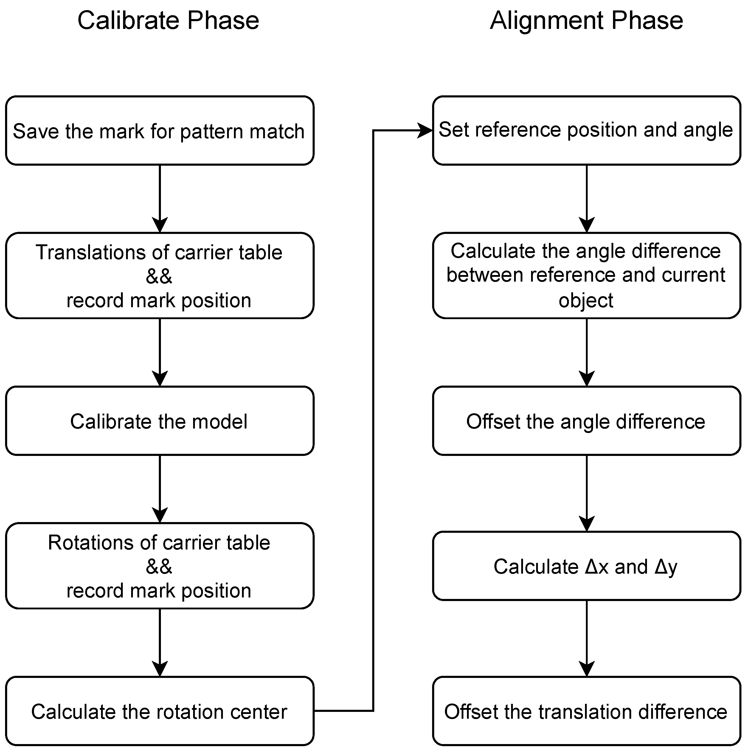
2.2. Misalignment Correction

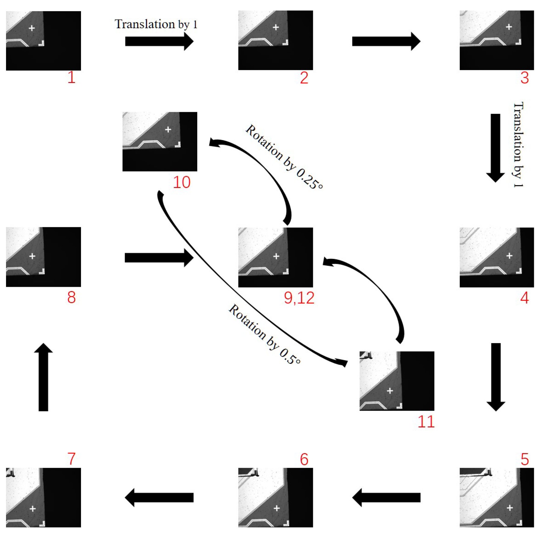
The pre-alignment camera installed on the carrier table is responsible for this process. The major procedure of the alignment correction is presented in Figure 6. A reference image is selected to prepare a matching template as a shape model. It normally chooses a distinguished shape in the region of interest (ROI) of the image as the feature mark. Figure 5 shows some different types of marks in the COG and FOG bonding process. Shape-based pattern search is a technique that detects reference marks automatically. We use this way to generate a shape model by specifying the range of rotations of the mark, the contrast of the local gray value, and the minimum size of the object. In most cases, we choose the center of the mark as the feature point after the matching process.
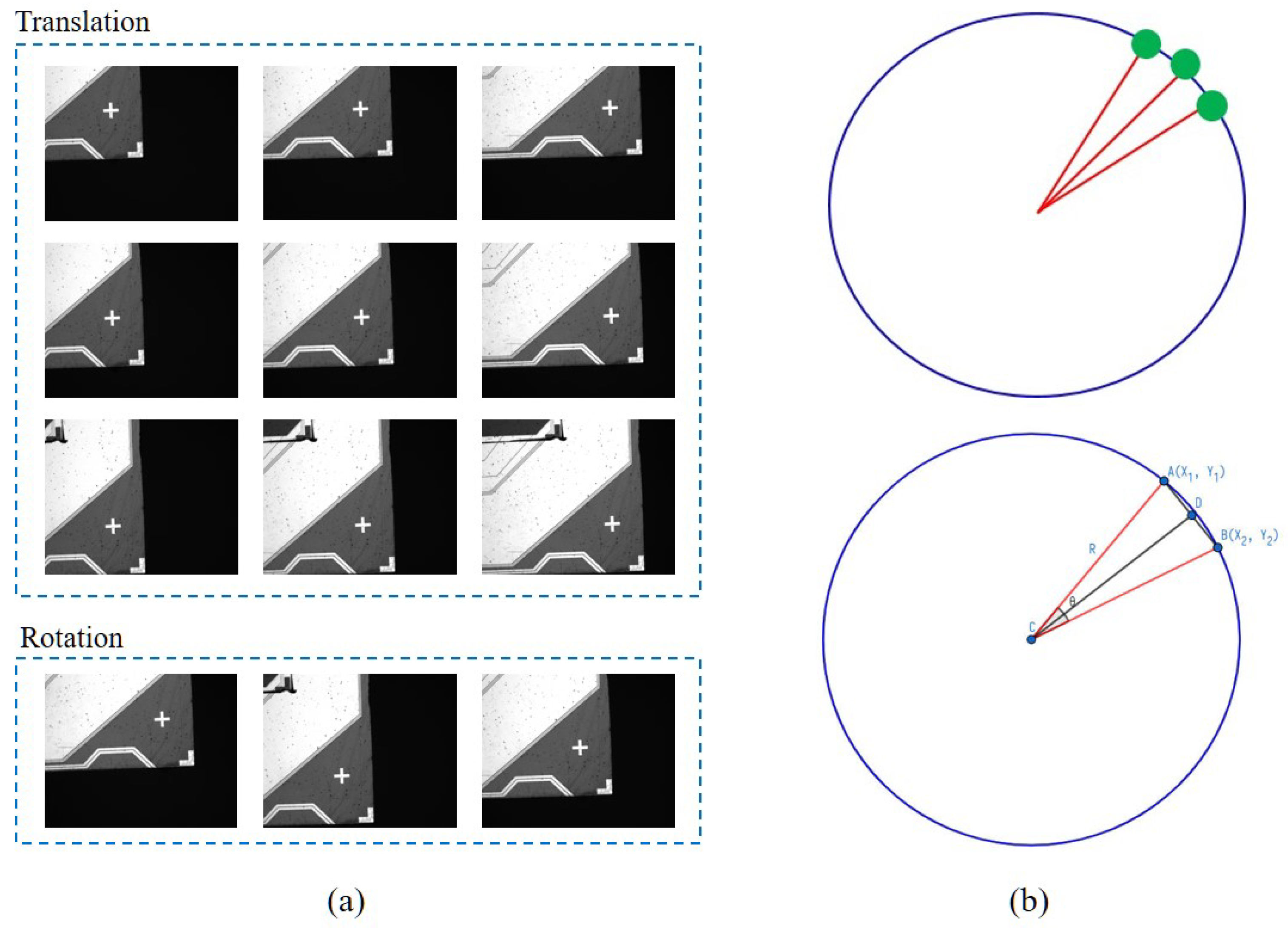
A 12-point calibration method is introduced to auto-calibrate the camera system and calculate the rotation center of the carrier table simultaneously, from which nine points are used to calculate a homogeneous transformation matrix based on Zhang’s method [27], and three points for finding the center of rotation. Such twelve points are derived from different images that are acquired in nine positions and three different angles. Figure 7 shows a sample of twelve images, in which the feature points of the mark are searched based on the described pattern search technique. The center of the mark region is chosen as the feature point. After recording the coordinates of feature points, the corresponding positions of these feature points in the world coordinate were then calculated through the homogeneous transformation matrix.
The homogeneous transformation matrix stands for a correspondence between different coordinate systems which can be shown in Equation (1). The image point and the transformed point in the real world are denoted as ( x i , y i ) , ( X i , Y i ) in homogeneous coordinates.
X i Y i 1 = H M a t 2 d · x i y i 1
A simplified transformation matrix that only consists of translation and rotation is represented as the Equation (2). T x and T y are the translation in the X- and Y- axis directions and r a r d denote the rotation parameters.
H M a t 2 d = r a r b T x r c r d T y 0 0 1
For a test subject, nine translation images and three rotation images are captured by controlling the motion of the carrier table. In each position, the coordinate of the feature point in the image space is measured by searching reference marks in view of an image while the corresponding location in the real world is recorded. The rotation angle of the carrier table is also included during this procedure. Nine of these pairs of points are used to approximate the transformation matrix which is expected to minimize the distance error between those pairs of points following the Equation (3).
m i n i X i Y i 1 H M a t 2 d · x i y i 1 2
Once the calibration process is finished, one point in image space can be transformed into that in the real world, thus enabling the calculation of the physical rotation center.
The rest three points are then offered to find the center of rotation. As a rotating angle can have an effect on the position of points in both X- and Y-axis directions, it is necessary to correct the angle deviation before translating the tested object to align with the reference one. Due to a different design of the mechanic structure, the rotation center of the carrier table can vary a lot, which leads to different impacts on the deviation of points. The main idea of calculating the rotation center of the carrier table, known as fitting a circle, is to obtain multiple points by rotating the carrier table and calculating the point of the circle which is supposed to cover those points in the real world. This method is based on an assumption that a pure rotational motion should form a track of a circle for a point on the plane. Given that we can acquire the physical rotation angle of the carrier table, the center of the circle can be calculated by each two of the three points as well as their included angle.
As demonstrated in Figure 7b, A ( X 1 , Y 1 ) and B ( X 2 , Y 2 ) are two points transformed from image space to the real-world coordinates. The midpoint D ( X 0 , Y 0 ) of the line AB through ( X 1 , Y 1 ) and ( X 2 , Y 2 ) is ( X 1 + X 2 2 , Y 1 + Y 2 2 ) , from which we can form the parametric equation of perpendicular bisector through C and D.
X = X 0 + t Δ X Y = Y 0 + t Δ Y
Because line CD is perpendicular to line AB, the slope of CD is reciprocal to that of AB, which can be expressed as
Δ Y Δ X = 1 Y 1 Y 2 X 1 X 2 = X 1 X 2 Y 1 Y 2
Therefore, Equation (4) can be transformed into
X = X 1 + X 2 2 + t ( Y 1 Y 2 ) Y = Y 1 + Y 2 2 + t ( X 1 X 2 )
Additionally, we can obtain the following equation from the lengths of AD and CD and their included A C D
A D = X 1 X 1 + X 2 2 2 + Y 1 Y 1 + Y 2 2 2 = ( X 1 X 2 ) 2 + ( Y 1 Y 2 ) 2 4 C D = ( t ( Y 1 Y 2 ) 2 ) + ( t ( X 1 X 2 ) 2 ) = t 2 ( X 1 X 2 ) 2 + ( Y 1 Y 2 ) 2 A C D = θ 2 = arctan A D C D = arctan 1 2 t
Therefore, we can derive the relationship between t and the included angle θ as
t = cos θ 2 2 sin θ 2 = sin θ 2 ( 1 + cos θ )
Therefore, we have
C x = X 1 + X 2 2 + s i n θ ( Y 1 Y 2 ) 2 ( 1 c o s θ ) C y = Y 1 + Y 2 2 + s i n θ ( X 1 X 2 ) 2 ( 1 c o s θ ) R = ( X 1 C x ) 2 + ( Y 1 C y ) 2
where ( C x , C y ) represents the center of the fitting circle and R specifies the radius. Three centers are given through the formula above and averaged to improve the accuracy of the center of the fitting circle.
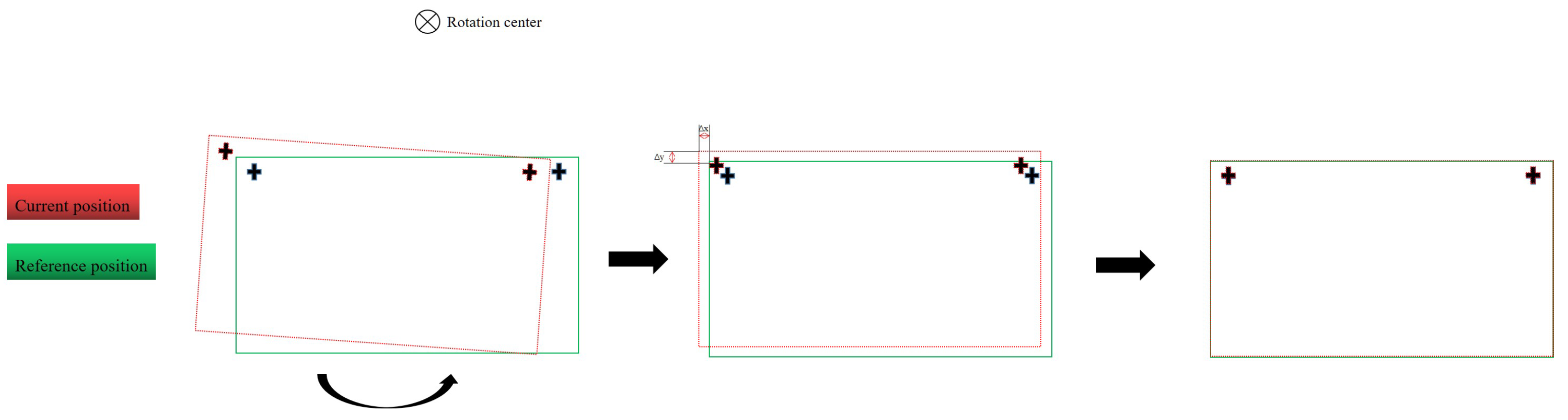
According to the flowchart in Figure 6, in the alignment phase, we first measure the angle of the reference image whereby we can obtain the deviation of the angle between the test image and the reference one. The camera can take images on the left and right side of the LCD module, respectively. Through searching for the feature marks printed on both sides, two feature points can be drawn to form a line that can act as a baseline. To compare the different angles of two lines, points have to be transformed to a uniform world coordinate. The transformed positions are then normalized by rotation center ( C x , C y ) to take the center as the origin point. By calculating θ t and θ c for reference angle and current angle, the difference of angle can be represented as Δ θ = θ t θ c . Secondly, the offset of translation is determined. Based on the design that the center of rotation is the origin of the coordinate, the radius and angle of a point in polar coordinate can be expressed as
r = X c 2 + Y c 2 , θ = arctan Y c X c
Then, the rotated points ( X r , Y r ) can be obtained by
X r = r c o s ( θ + Δ θ ) Y r = r s i n ( θ + Δ θ )
Either point of left or right side feature point can be used to calculate the offset of translation. We use ( X r , Y r ) and ( X t , Y t ) to denote rotated point by Δ θ and the reference point, respectively. Finally, the translation offset can be obtained by
Δ X = X r X t Δ Y = Y r Y t
After determining the rotation center and the translation offset, the tested module can be aligned to the reference position as Figure 8 shows.

2.3. Bump Positioning

After aligning the test object with the reference one, the positional deviation can be reduced thus contributing to accurately positioning bump areas containing the particles to be detected. The aligned LCD module is scanned by a line scan camera installed under the carrier table. 
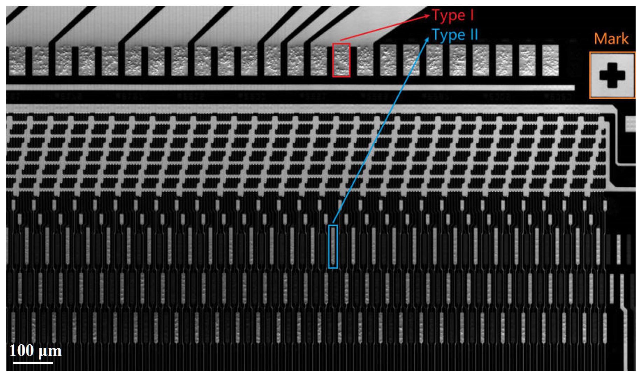
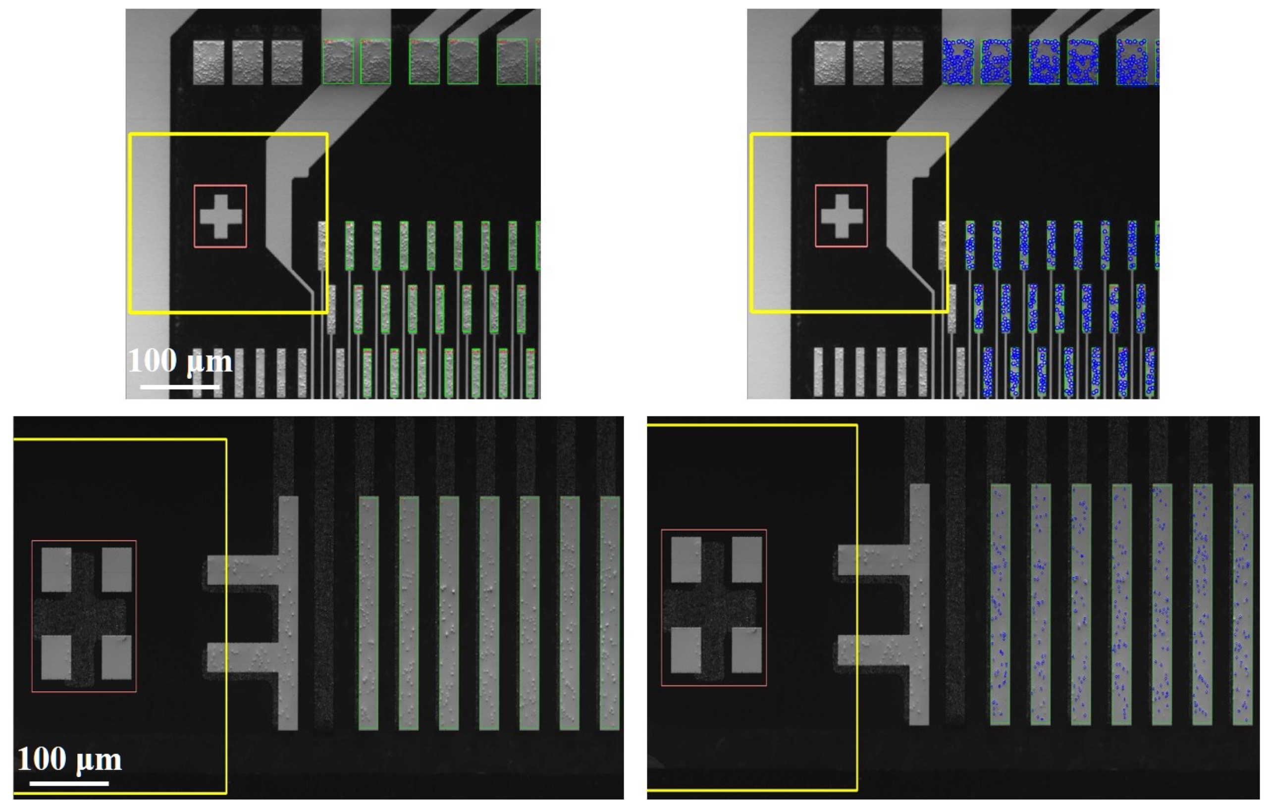
Figure 9 shows a scanned image in the COG process. The cross-shaped pattern on the top right of the image serves as the positioning mark, while the red and blue regions in the image stand for ITO bumps. Two major types of bumps are annotated in Figure 9, which are block-like regions for type I and bar-like regions for type II, respectively.
As a whole imaging region consists of numerous bumps and other irrelevant pixels that make up a large portion of the image, it is difficult and time-consuming to extract valid information. Bump positioning intends to segment essential regions from the whole image and allows the detection algorithm to operate on every smaller region, which can reduce the size of detection areas and improve efficiency. Considering that the bump positions of a type of component are relatively fixed, we can construct a standard file with position information of all bump areas in it. Such information can be stored in the form of values relative to the position of the mark, which can be quickly determined by the shape-based match method. The feature mark is first searched in the test image, then the bump areas can be annotated with information in the standard file. The standard file can also be finetuned to adapt to the bump distribution in different LCD modules.

2.4. Particle Detection

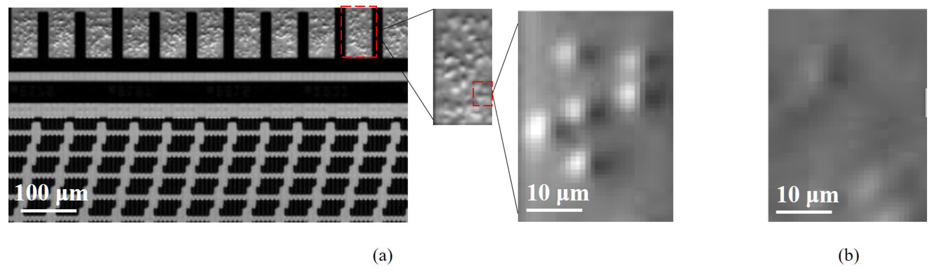
The number of particles captured is calculated in every segmented area of the bump. ACF conductive particles represent microspheres and deform with different levels of press strength. During the bonding process, these particles are trapped between the bump areas, causing those areas to show uneven pits. Figure 10a extracts a sample of well-deformed conductive particles, while (b) shows a local image of particles taken under the inappropriate pressure condition.
We can observe that the properly pressed particles appear as distinct light and dark parts in the image, while over-deformed particles have a weak contrast compared with neighbor areas. Based on such an observation, the particle areas are intended to be recognized by locating the extreme point of gray value of every particle. However, many false extreme points occur possibly caused by sharp changes in the gray-scale values of the edge of the bump or the intersection area between particles.
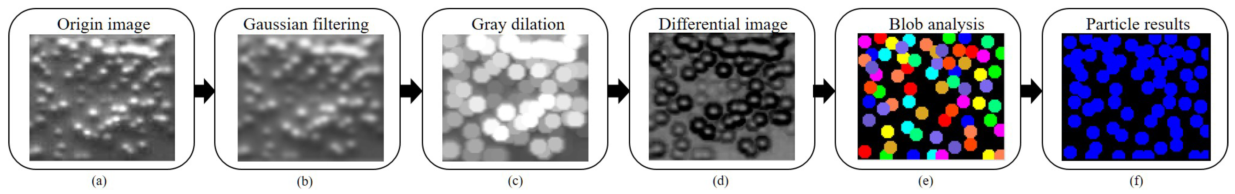
To reduce the effect of edge and intersection area on the detection accuracy, we first smooth the original image Figure 11a by the gaussian kernel, as shown in Figure 11b. We denote the original image as I ( x , y ) and the smoothed image as I g ( x , y ) . During the smoothing process, the original image is filtered by the 2D gaussian kernel G ( x , y ) which can be formulated as the Equation (13)
G ( x , y ) = 1 2 π σ 2 exp x 2 + y 2 2 σ 2
where x is the distance from the origin in the horizontal axis, y is the distance from the origin in the vertical axis. The smoothed image can be denoted as
I g ( x , y ) = I ( x , y ) G ( x , y ) .
Subsequently, we perform a gray value dilation on the smoothed image with a structuring element b in order to highlight the region of each particle. An example of output image after the gray value dilation is shown in Figure 11c. The gray-scale value of the dilated image is defined with the maximum value of the overlapped region between the structuring element and the target image. Such processing can be demonstrated as
[ I b ] ( x , y ) = m a x ( s , t ) b   I ( x s , y t )
where s and t denote the distance from the origin in both directions. According to the size of structuring element b, the s and t should be in [ s i z e , s i z e ] . We can regard the structuring element as another filtering kernel because it serves to further reduce the variation of local gray values. As a result, the gray values of a particle region are equivalent to the maximum value of this region, which is usually the gray value of the center of the particle. Following the process in Figure 11d, the dilated image is compared with the smoothed image to create a differential image where the extreme points of every particle are expected to be emphasized. To achieve this, we normalize the mean gray value of the smoothed image to 128 following the Equation (16)
I g ( x , y ) = I g ( x , y ) × 128 M e a n
then the differential image I d ( x , y ) is created by the Equation (17).
I d ( x , y ) = I g ( x , y ) [ I b ] ( x , y ) + 128
In the differential image, the central parts of particles are brighter than neighbor pixels indicating the existence of particles.
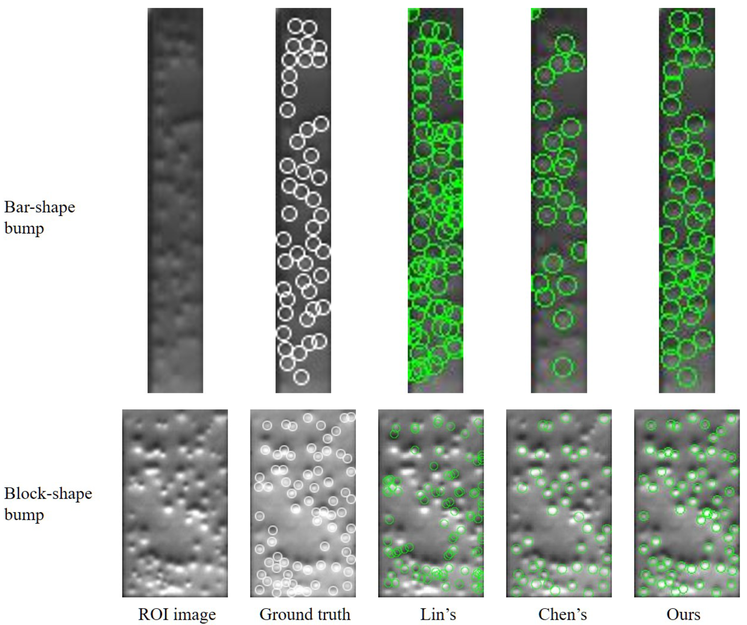
To refine the detection result, we also adopt the blob analysis to exclude noisy objects. During the blob analysis, detected objects are checked case by case, such as a sample shown in Figure 11e. Some gray features of particles can be used to enhance the reliability of the detection result. For example, the gray strength of the particle is assumed to exceed a certain threshold while the result with a lower strength should be removed. In addition, since the standard deviation of the brightness in the particle region should be within a certain range, we can extract the particle objects based on this criterion. After excluding noisy objects, the detection results in Figure 11f can be visualized by the detected centers of particles and a specified particle radius.
The number and density of particles in a given region can be determined from the results depicted in Figure 11f. Normal particles tend to be numerous and have a relatively uniform and dense distribution, while over-deformed particles can be identified by a small number of particles and a sparse distribution in the image analysis. In practical production, the threshold for distinguishing between normal and over-deformed particles should be determined based on the specific criteria of the plant.

3. Results and Discussion

3.1. Experiment Setup

As depicted in Figure 4, the majority of the system consists of mechanical components and sensor sets. The mechanical components primarily consist of robotic grippers responsible for loading and unloading LCD modules, a carrier platform equipped with translation and rotation motors, and a large horizontal track providing X-axis movement for pre-alignment cameras. The sensor sets, including the pre-alignment camera, line scan camera, and laser displacement sensor, are essential tools in the detection system. A detailed configuration can be found in Table 1. In terms of the parameters for the detection algorithm, a Gaussian kernel with a size of 3 × 3 and a σ of 0.6 was chosen, and the structuring element employed a circle with a radius of 8 pixels. In the blob analysis, the strength threshold of particles is set to 8, and the range of brightness within a particle region is 20–220.

3.2. Calibration Result

In our experiment, we first calibrated the homogeneous transformation matrix between the image space and the world coordinate and calculated the center of rotation of the carrier table. In Figure 12, we show the relationship between the captured images in terms of physical position, where subfigures 1–9 are captured by translating the carrier by 1 mm, while subfigures 10–12 are captured by rotating the carrier by 0.25 .
Table 2 shows the pixel location and the physical location of twelve images. The calibration result is shown in the last column. The location and rotation in the world coordinate were determined by the relative distance to the origin of the carrier table. We derived the homogeneous transformation matrix H M a t 2 d through images 1–9 while calculating the center of rotation through images 10–12. As the center of rotation of the carrier platform was far from the location of captured images, three centers were calculated by two images and the included angle following the Equation (9) and then averaged to the final center.

3.3. Alignment Result

We selected some test samples to check the precision of our proposed method. Samples were acquired by controlling the machine to move different offsets in Y-axis or around the rotating axis while related information is recorded. This motion was conducted to simulate the occasion when the robotic gripper fails to make sure that the LCD module keeps the same position as the standard module.
In our experiments, the line scan camera was installed at the X-axis. We moved the line scan camera and took images of the left panel and right panel containing the feature marks. The mark locations in both panels were recorded and compared with those in the reference panel. Table 3 presents the positions of the left and right markers in various settings, with the positions being unified to a coordinate system with the center of rotation of the carrier table serving as the origin. For example, Y0.3 moves the carrier platform in the Y-axis direction by 0.3 mm, and Y0.6-R0.3 moves 0.6 mm alongside the Y-axis and rotates 0 . 3 around the center of rotation of the carrier table.
Table 4 demonstrates the alignment precision as below. The rightmost column shows the difference between the alignment result and previously recorded information, which represents Δ X , Δ Y , and Δ θ , respectively. Such results show that our method achieves high precision in restoring the offset of translation and rotation of tested modules.
Although the setting of the X-axis was not verified separately, the offset of the X-axis was also calculated simultaneously during the verification of Y and θ . Considering the similarity of the X-axis and Y-axis, the experimental results can also illustrate the alignment accuracy of the X-axis.
Furthermore, we collected all data in three groups listed in Table 5 and analyzed how different offsets can affect the accuracy of our proposed method. We can observe from this table that our alignment method can keep a stable result in pure translation or rotation.

3.4. Detection Results

We evaluated the effectiveness of the proposed method in bump areas acquired from both COG and FOG samples. Figure 13 shows the results of particle detection in COG and FOG, respectively. Bump areas were segmented according to the saved file about the relative position of bumps to the feature mark in different types of samples such as COG and FOG. Two major types of bumps were categorized the bar-shape and the block-shape. The bar-shape bump is long and narrow, while the block-shape bump is short and wide that contains relatively dense particles. The target area of the block-shaped bump is smaller in size and the visibility of particles is weaker, thus making it more difficult to accurately inspect the number of particles.
Figure 14 looks closer at bar-like bump areas. Bumps with an insufficient number of particles would be sent to NG output based on the manufacturer’s requirement.
We also compared our method with Lin’s [12] and Chen’s [26] method and verified the effectiveness of our method as shown in Figure 15. Lin’s method was sensitive to slight changes in gray value, thus causing the algorithm to detect more particles in regions where particles overlap densely. Such a method treated the NG module as the OK module and may produce many false positive samples, which is inappropriate in the practical industry. Contrarily, Chen’s method recognized the number of overlapped particles more accurately. However, the performance of Chen’s method depended on the initialization of the cluster center and thus may lose a number of particles on some occasions.
The detection result in 433 particle samples of bar-shape bumps and 629 samples of block-shape bumps are shown in Table 6. Lin’s method demonstrates a slightly improved recall rate for bar bumps due to its tendency to generate more particle candidates than are actually present, thereby covering a larger portion of the region on samples with smaller dimensions. Conversely, this method exhibits a significant decline in recall performance on samples with larger dimensions, such as the block-shape bumps. Combined with the low precision, Lin’s method shows a high over-checking rate which will allow a number of false products to be passed and affect negatively quality control. Chen’s precision rate is good but the number of detected particles is lower than that in other methods when the gray-scale value of the image is weak. In contrast, our method balances the precision and recall rate of the detection result and performs better than the aforementioned methods.

4. Conclusions

In this paper, we establish an automatic inspection system to serve multiple bonding processes such as COG and FOG in LCD module manufacturing. A 12-point calibration method is developed to adaptively control the position and rotation of the carrier table and to alleviate the high requirement of assembly accuracy. This method can complete the alignment by taking images once, which calculates a homogeneous transformation matrix with nine pairs of points and determines the center of rotation with extra three pairs of points. In our experiments, the alignment error can be less than 0.05 mm.
This study also proposes an automatic particle detection method based on gray morphology which achieves a fast and robust inspection of the number of conductive particles trapped in bump areas of the anisotropic conductive film. Based on the observation that the central part of conductive particles is brighter than the neighbor region in grayscale under our DIC imaging model, we apply the gray dilation method to the whole image and subtract dilated image from the original input, from which the center regions of particles are stressed out. Our experiments have examined the effectiveness of this method, in which the precision rate is 93%, while the recall rate is 92.4%. As our proposed detection method depends on finding the difference between the central and peripheral regions of particles, the overlap of multiple particles may intervene in this difference, thus creating an obstacle to accurate segmentation. In the future, further research will be conducted to improve the representation of particles and segment those overlapped particles more accurately.

Author Contributions

Conceptualization, T.L.; methodology, F.Z.; software, T.L. and F.Z.; validation, T.L.; formal analysis, F.Z.; resources, Z.Z.; writing—original draft preparation, T.L.; writing—review and editing, F.Z., H.Y. and H.L.; visualization, T.L.; supervision, F.Z. and Z.Z.; funding acquisition, Z.Z. All authors have read and agreed to the published version of the manuscript.

Funding

This work is supported by the National Key Research and Development Program of China (2022YFB3303800), the National Natural Science Foundation of China (U21A20482, U1909218), the Science Technology Project funding from Binzhou Weiqiao Guoke Advanced Technology Research Institute(E2D21709, E2D21710, E2D21711).

Data Availability Statement

Not applicable.

Conflicts of Interest

The authors declare no conflict of interest.

Abbreviations

The following abbreviations are used in this manuscript:
LCDLiquid Crystal Display
ACFAnisotropic Conductive Film
ICIntegrated Circuit
FPCFlexible Printed Circuit
ITOIndium Tin Oxide
COGChip-on-Glass
FOGFlex-on-Glass
DICDifferential Interference Contrast
ROIRegion of Interest

References

  1. Gao, L.L.; Chen, X.; Zhang, S.B.; Gao, H. Mechanical properties of anisotropic conductive film with strain rate and temperature. Mater. Sci. Eng.-Struct. Mater. Prop. Microstruct. Process. 2009, 513–514, 216–221. [Google Scholar] [CrossRef]
  2. Paik, K.W.; Yim, M.J. New anisotropic conductive adhesives for low cost and reliable flip chip on organic substrates applications. In Proceedings of the International Symposium on Electronic Materials and Packaging (EMAP2000), Hong Kong, China, 30 November–2 December 2000; pp. 282–288. [Google Scholar]
  3. Paik, K.W.; Yim, M.J.; Kwon, W.; Smta, S. Significant reliablity enhancement using new anisotropic conductive adhesives for flip chip on organic substrates applications. In Proceedings of the 6th Annual Pan Pacific Microelectronics Symposium, Kauai, HI, USA, 13–16 February 2001; pp. 217–223. [Google Scholar]
  4. Mou, Y.; Zhang, Y.; Cheng, H.; Peng, Y.; Chen, M. Fabrication of highly conductive and flexible printed electronics by low temperature sintering reactive silver ink. Appl. Surf. Sci. 2018, 459, 249–256. [Google Scholar] [CrossRef]
  5. Mou, Y.; Cheng, H.; Wang, H.; Sun, Q.; Liu, J.; Peng, Y.; Chen, M. Facile preparation of stable reactive silver ink for highly conductive and flexible electrodes. Appl. Surf. Sci. 2019, 475, 75–82. [Google Scholar] [CrossRef]
  6. Shiozawa, N.; Isaka, K.; Ohta, T. Electric properties of connections by anisotropic conductive film. J. Electron. Manuf. 1995, 5, 33–37. [Google Scholar] [CrossRef]
  7. Yim, M.J.; Hwang, J.; Paik, K.W. Anisotropic conductive films (ACFs) for ultra-fine pitch Chip-On-Glass (COG) applications. Int. J. Adhes. Adhes. 2007, 27, 77–84. [Google Scholar] [CrossRef]
  8. Chin, M.; Hu, S.J. A multiple particle model for the prediction of electrical contact resistance in anisotropic conductive adhesive assemblies. IEEE Trans. Components Packag. Technol. 2007, 30, 745–753. [Google Scholar] [CrossRef]
  9. Shi, F.G.; Abdullah, M.; Chungpaiboonpatana, S.; Okuyama, K.; Davidson, C.; Adams, J.M. Electrical conduction of anisotropic conductive adhesives: Effect of size distribution of conducting filler particles. Mater. Sci. Semicond. Process. 1999, 2, 263–269. [Google Scholar] [CrossRef]
  10. Yen, Y.W.; Lee, C.Y. ACF particle distribution in COG process. Microelectron. Reliab. 2011, 51, 676–684. [Google Scholar] [CrossRef]
  11. Xie, B.; Shi, X.Q.; Ding, H. Investigation of mechanical and electrical characteristics for cracked conductive particle in anisotropic conductive adhesive (ACA) assembly. IEEE Trans. Components Packag. Technol. 2008, 31, 361–369. [Google Scholar]
  12. Lin, C.S.; Huang, K.H.; Lin, T.C.; Shei, H.J.; Tien, C.L. An automatic inspection method for the fracture conditions of anisotropic conductive film in the TFT-LCD assembly process. Int. J. Optomechatronics 2011, 5, 286–298. [Google Scholar] [CrossRef]
  13. Ni, G.; Liu, L.; Du, X.; Zhang, J.; Liu, J.; Liu, Y. Accurate AOI inspection of resistance in LCD Anisotropic Conductive Film bonding using differential interference contrast. Optik 2017, 130, 786–796. [Google Scholar] [CrossRef]
  14. Ni, G.; Liu, L.; Zhang, J.; Liu, J.; Liu, Y. Analysis of trapped conductive microspheres in LCD FOG anisotropic conductive film bonding. In Proceedings of the 2nd IEEE Advanced Information Technology, Electronic and Automation Control Conference (IAEAC), Chongqing, China, 25–26 March 2017; pp. 1414–1420. [Google Scholar]
  15. Ni, G.; Liu, L.; Zhang, J.; Liu, J.; Wang, X.; Du, X.; Yue, H.; Liu, Y. Automatic optical inspection of bump offsets in flex-on-glass bonding using differential interference contrast imaging. Int. J. Precis. Eng. Manuf. 2020, 21, 177–187. [Google Scholar] [CrossRef]
  16. Sheng, X.; Jia, L.; Xiong, Z.; Wang, Z.; Ding, H. ACF-COG interconnection conductivity inspection system using conductive area. Microelectron. Reliab. 2013, 53, 622–628. [Google Scholar] [CrossRef]
  17. Yim, M.J.; Paik, K.W. Design and understanding of anisotropic conductive films (ACF’s) for LCD packaging. IEEE Trans. Components Packag. Manuf. Technol. Part A 1998, 21, 226–234. [Google Scholar]
  18. Ni, G.; Du, X.; Liu, L.; Zhang, J.; Liu, J.; Liu, Y. Automated optical inspection of liquid crystal display anisotropic conductive film bonding. Opt. Eng. 2016, 55, 103109. [Google Scholar] [CrossRef]
  19. Ni, G.; Liu, L.; Zhang, J.; Liu, J.; Liu, Y. High-resolution imaging optomechatronics for precise liquid crystal display module bonding automated optical inspection. J. Electron. Imaging 2018, 27, 013013. [Google Scholar] [CrossRef]
  20. Lin, C.S.; Huang, K.H.; Lay, Y.L.; Wu, K.C.; Wu, Y.C.; Lin, J.M. An improved pattern match method with flexible mask for automatic inspection in the LCD manufacturing process. Expert Syst. Appl. 2009, 36, 3234–3239. [Google Scholar] [CrossRef]
  21. Kim, H.T.; Yang, H.J.; Baek, S.Y. Iterative algorithm for automatic alignment by object transformation. Microelectron. Reliab. 2007, 47, 972–985. [Google Scholar] [CrossRef]
  22. Lin, C.T.; Yu, Y.C. Visual servoing for mask alignment in photolithography positioning system. In Proceedings of the IEEE International Conference on Mechatronics (ICM), Taipei, Taiwan, 10–12 July 2005; pp. 762–767. [Google Scholar]
  23. Sun, W.; Zhang, Z.; Zhang, W. A coaxial alignment method for large flange parts assembly using multiple local images. IEEE Access 2021, 9, 16716–16727. [Google Scholar] [CrossRef]
  24. Kim, J. New wafer alignment process using multiple vision method for industrial manufacturing. Electronics 2018, 7, 39. [Google Scholar] [CrossRef] [Green Version]
  25. Algorri, J.F.; Bennis, N.; Urruchi, V.; Morawiak, P.; Sánchez-Pena, J.M.; Jaroszewicz, L.R. Tunable liquid crystal multifocal microlens array. Sci. Rep. 2017, 7, 17318. [Google Scholar] [CrossRef] [PubMed] [Green Version]
  26. Chen, Y.; Xiao, K.; Guo, Z.; He, J.; Liu, C.; Chen, S. Detection of conducting particles bonding in the circuit of liquid crystal display. Chin. J. Liq. Cryst. Displays 2017, 32, 553–559. [Google Scholar] [CrossRef]
  27. Zhang, Z.Y. A flexible new technique for camera calibration. IEEE Trans. Pattern Anal. Mach. Intell. 2000, 22, 1330–1334. [Google Scholar] [CrossRef]
Figure 1. ACF can reduce the size of the LCD module and achieve a higher level of integration.
Machines 11 00049 g001
Figure 2. (a) Demonstrates the diagram of the bonding process; (b) is zoomed in to show the composition of the ACF.
Machines 11 00049 g002
Figure 3. (a) Explains the conductivity principle of the ACF; (b) shows part of the bump areas after the bonding process.
Machines 11 00049 g003
Figure 4. An overview of the automatic inspection system which mainly includes conveyor modules, pre-alignment modules, CCD inspection modules, carrier modules, and NG output modules. Tested LCD modules are first aligned by the misalignment correction algorithm, then the bump images are acquired by the CCD line scan camera, and finally, the conductive particles are detected.
Machines 11 00049 g004
Figure 5. Different shapes of marks: (a) represents a cross mark; (b) represents a dark cross sandwiched between four bright squares; (c) represents a square surrounded by four triangles. The mark shape can be used according to practical manufacturer setting. We can extract the center of the marker as the key point for calibration and alignment.
Machines 11 00049 g005
Figure 6. This flowchart indicates the steps to simultaneously calibrate the camera and calculate the center of rotation of the machine.
Machines 11 00049 g006
Figure 7. (a) Uses the 12-point misalignment correction method to determine the center of rotation and to calculate the offset of translation. These twelve sample images are taken by a pre-alignment camera installed above the carrier table; (b) calculates the physical rotation center on the occasion of a large radius and a small angular interval.
Machines 11 00049 g007
Figure 8. Expected result after the misalignment correction process.
Machines 11 00049 g008
Figure 9. The local image of LCD module containing bump and mark areas.
Machines 11 00049 g009
Figure 10. (a) Well deformed conductive particles; (b) over-deformed particles.
Machines 11 00049 g010
Figure 11. This flowchart shows the procedure of particle detection. The original image (a) is smoothed to image (b), (b) is dilated by a structuring element to produce (c), (d) highlights the particle centers, (e) remove noisy objects by features of the particle, and the final result is presented in (f). The processing and visualization of images are supported by OpenCV.
Machines 11 00049 g011
Figure 12. The relationship between the captured images in terms of physical position.
Machines 11 00049 g012
Figure 13. The first row is a part of the bump area of the COG sample (left) and the corresponding result (right), while the second row displays the input and output of the FOG test in the same order.
Machines 11 00049 g013
Figure 14. A closer view of the result of particle counts in bar-shape bump areas. The first row is the raw image while the second row is the detection result.
Machines 11 00049 g014
Figure 15. Examples of different detection methods on bar-shape bumps and block-shape bumps.
Machines 11 00049 g015
Table 1. Parameters and manufacturers of major modules in the inspection system.
CategoryModel NumberManufacturerProperties
X-axis linear actuatorGTH5 seriesTOYOStroke length: 500 mm
Y-axis linear actuatorETH14 seriesTOYOStroke length: 500 mm
Θ -axis direct drive rotary motorLD seriesZCOEAngular accuracy: ± 30
Angular repeatability: ± 2 . 5
Pre-alignment cameraMV-CA013 seriesHIKROBOTResolution: 1280 × 1024
Max. frame rate: 90 fps
TDI line scan cameraVT-3K7C seriesVieworksResolution: 3200
Line rate: 100 khz
Laser displacement sensorZS-HLDC/LDC SeriesOmronMax. resolution: 0.25 μ m/px
Max. response speed: 110 μ s
Table 2. The pixel location and the physical location of twelve images and the calibration result.
Image IndexX in Pixel (px)Y in Pixel (px)X in Carrier (mm)Y in Carrier (mm) θ in Carrier ( )Result (mm)
1451.501703.999−26.4627325.34940HMat2d 1
2657.752695.463−27.4627325.34940
3862.519688.233−28.4627325.34940
4855.523481.747−28.4627324.34940
5846.937278.084−28.4627323.34940
6642.295285.407−27.4627323.34940
7436.527292.669−26.4627323.34940
8444.942497.018−26.4627324.34940
9649.725490.896−27.4627324.34940
10780.087301.71−27.4627324.3494−0.25 C x = 160.812
11518.451678.46−27.4627324.34940.25 C y = 182.984
12649.441490.792−27.4627324.34940R = 235.439
1  H M a t 2 d = 0.00486334 0.000181669 24.3918 0.000180196 0.00486517 321.846 0 0 1 .
Table 3. The positions of the left and the right mark (unit:mm).
SettingLeft MarkRight Mark
Ref. ( 188.223 , 141.469 ) ( 538.615 , 141.469 )
Y0.3 ( 187.458 , 143.135 ) ( 537.734 , 141.295 )
Y0.6 ( 188.265 , 142.068 ) ( 538.535 , 142.064 )
R0.1 ( 187.995 , 141.828 ) ( 538.264 , 141.21 )
R0.3 ( 187.455 , 142.542 ) ( 537.729 , 140.702 )
Y0.6-R0.3 ( 187.458 , 143.135 ) ( 537.734 , 141.295 )
Table 4. The result of misalignment correction in different settings (unit: Δ X ( m m ) , Δ Y ( m m ) , Δ θ ( ) ).
SettingLeft PanelRight PanelResult
  Ref.Machines 11 00049 i001Machines 11 00049 i002 Δ X = 0 Δ Y = 0 Δ θ = 0
  Y0.3Machines 11 00049 i003Machines 11 00049 i004 Δ X = 0.046 Δ Y = 0.294 Δ θ = 0.001
  Y0.6Machines 11 00049 i005Machines 11 00049 i006 Δ X = 0.043 Δ Y = 0.596 Δ θ = 0.001
  R0.1Machines 11 00049 i007Machines 11 00049 i008 Δ X = 0.042 Δ Y = 0.002 Δ θ = 0.1
  R0.3Machines 11 00049 i009Machines 11 00049 i010 Δ X = 0.035 Δ Y = 0.004 Δ θ = 0.301
  Y0.6-R0.3Machines 11 00049 i011Machines 11 00049 i012 Δ X = 0.035 Δ Y = 0.588 Δ θ = 0.301
Table 5. The impact of different offset configurations on the accuracy of the alignment algorithm (unit: X ( m m ) , Y ( m m ) , θ ( ) ).
ConfigurationXY θ Δ X Δ Y Δ θ diff Xdiff Ydiff θ
Y0.3100.300.0460.2940.0020.0460.0060.002
Y0.600.600.0440.5960.0010.0440.0040.001
Y0.900.900.0450.8970.0010.0450.0030.001
R0.1000.10.0430.0020.1010.0430.0020.001
R0.2000.20.040.0020.2010.040.0020.001
R0.3000.30.0360.0040.3010.0360.0040.001
Y0.3-R0.200.30.20.0380.2980.2010.0380.0020.001
Y0.6-R0.200.60.20.0420.5910.20.0420.0090
Y0.6-R0.300.60.30.0350.5880.3010.0350.0120.001
1 Different colors are used to denote the relevance of the results. For instance, the red text “Y0.3” signifies an offset of 0.3 mm along the Y-axis, with a corresponding difference in the result of “0.006”.
Table 6. The comparison of detection results of different methods.
Bump TypeMethodDetected NumberRight ResultPrecisionRecallCalculation Time (ms)
Bar-shapeLin’s88440245.5%92.8%13.3
Chen’s25621885.2%50.3%43.2
Ours43040093%92.4%1.2
Block-shapeLin’s87046453.3%73.8%15.15
Chen’s38235392.4%56.1%57.7
Ours56453795.2%85.4%5.5
Disclaimer/Publisher’s Note: The statements, opinions and data contained in all publications are solely those of the individual author(s) and contributor(s) and not of MDPI and/or the editor(s). MDPI and/or the editor(s) disclaim responsibility for any injury to people or property resulting from any ideas, methods, instructions or products referred to in the content.

