1. Introduction
In the modern era, the environment is prone to pollution caused due to various aspects, especially vehicles powered by fossil fuels. As the pollution prone system is becoming of greater concern, replacing these vehicles with plug-in electric vehicles (PEV) is becoming an attractive proposition. To take this technology forward to next level of sophistication, one needs to provide not only an optimal charging system, but also the most effective power conditioning unit to drive the motor more effectively. This results in more flexibility for PHEV customers [
1,
2,
3,
4]. Usually, a bi-directional DC-DC converter (BDC) is associated with the design of charger as well as the power conditioning unit of an EV or PHEV, as shown in
Figure 1, as it allows bidirectional power flow (charging and discharging and similarly during motoring and braking periods respectively).
The broad categorization of these BDCs refers to isolated (transformer based) converters and non-isolated (transformer less) converters. Conventional isolated converters are used to meet the high gain requirements of EVs, which provides the flexibility of reduced operating voltages at the battery side in the design of EVs. For this purpose, step-up natured isolated converters, e.g., flyback, push-pull, current-fed half bridge, and current-fed full bridge topologies, are preferred with the adoption of a suitable transformer turns ratio. However, this solution suffers from large voltage spikes due to the leakage inductance of the transformer, in turn, leading to a power loss in the switch. Thus, non-isolated BDC is preferred when compared with isolated BDC, as it has several advantages, such as high efficiency, more reliability, and less component count, which lead to a reduced size and overall cost [
5,
6]. In general, high gain is obtained in the case of transformerless converters by having a high duty cycle. However, the price to pay is the increasing reverse recovery losses and reduced efficiency. Moreover, the reliability of the switches is also affected due to high voltage stress because of the high duty ratio. To overcome these issues, ample converter topologies have been proposed in the literature, namely cascading boost converters [
7], interleaving topology, soft switching technique to mitigate voltage spikes, and incorporating a coupled inductor in the conventional boost topologies [
8].
Among all, coupled inductor (CI) based topologies have received more attention to achieve high conversion gain due to their merits, such as compactness and high power density in both charging and discharging modes [
9,
10]. Moreover, such topologies can mitigate the disadvantages of both isolated and non-isolated BDC, such as voltage stresses, high voltage diversity factor with huge duty cycle, and high cost. However, there are still few more problems with CI--BDC converters, such as leakage energy due to the coupled inductor, causing voltage stress during the turn off process, apart from complexity in circuit design. To address this issue, the resistor-capacitor-diode (RCD) voltage-clamp technique is proposed. Apart from that, the Voltage-Clamp (VC)—CI--BDC converter has been proposed in [
11]. However, in all these topologies, a capacitor is placed at the output side [
12,
13,
14,
15,
16,
17,
18,
19,
20]. As the system in energized, the voltage levels increase to the rated value, thus enabling an inrush of current in uncharged output capacitors. The inrush current magnitude flowing inwards to the capacitors is proportional to the rate of change of voltage, as illustrated in Equation (1)
where
= inrush current produced by capacitance,
Co = total capacitance,
dVo = change in voltage across the capacitor, and
dt = rise time during voltage ramp up.
Two important factors of interest regarding inrush current are noteworthy. Firstly, the inrush current may exceed the rated value of currents in PCB modules, which can affect the power routing, and ultimately the overall system may deteriorate. However, if one designs by considering the maximum value of a large inrush current, the PCB component sizes will increase. Thus, the overall cost will increase, and resistance of the path will be affected. Secondly, the capacitor at the load side, when added, will cause instability when the capacitor is charged from the supply.
Inrush current minimization has been achieved by using a soft start technique which reduces the duty cycle and thus reduces the capacitor charging, which in turn minimizes the inrush current [
21,
22,
23]. However, this solution slows down the response, which in turn decreases the system dynamics. On the other hand, the other ways of reducing inrush current are voltage regulation, by the design of a discrete load switch and aggregate load switches [
24]. The discrete load switch method requires more components. The aggregate method requires a dc-dc converter to control multiple load switches. In both the cases, the inclusion of a load switch will result in greater ease of design but increase the component count and cost.
From Equation (1), it can be inferred that by minimizing the capacitor voltage, the inrush current can be minimized, which can be used as an alternative solution to the above-mentioned problem. This fact has motivated the derivation of a new converter, which can offer reduced voltage across the capacitor. In this regard, the capacitor clamped boost inverter (CCBI) concept has been found to be a suitable solution [
25]. However, this paper does not deal with the inrush concept and bi-directional power flow application in dc-dc power conversion. This knowledge gap has motivated the utilization of the CCBI concept along with the coupled inductor concept to derive a new converter and to carry out its performance investigation in the above-mentioned directions. This newly derived converter has been named the capacitor clamped coupled inductor BDC (CCCI--BDC). All the reviewed dc-dc power converter topologies have been presented as a flowchart in
Figure 2.
The organization of the paper is as follows.
Section 1 contains the introduction and thorough review of the state-of-the-art technologies.
Section 2 entails in-depth mathematical modeling along with various modes of operation and analysis of the proposed CCCI--BDC. The proposed converter performance improvement has been validated using simulation in a Simulink environment and verified through hardware implementation and performance investigation.
Section 3 describes simulation results and discussions.
Section 4 details experimental results and analysis.
Section 5 incorporates the conclusions.
2. Proposed System
The CI--BDC is an improvement over the conventional BDC, designed for high voltage variant applications. The main function of this coupled inductor is to absorb and deliver energy during the converter operating period. The power absorbed and released by the CI is not the same in all durations because of the operating conditions. By using CI, one can make the converter size compact as it uses a single core in place of multiple cores. In the literature concerning CI technology, a single core is treated as a Flyback transformer and the windings of CI behave as magnetic switches used to store and release energy. The conventional converter necessitates two capacitors (one
CHV for boost mode and another
CLV for buck mode respectively), but the proposed converter uses only one capacitor (
CC) to support both modes of operation [
11].
Figure 3 shows the proposed CICC--BDC with single voltage clamping, which is an improvement over the CI--BDC, proposed in [
11]. For simple analysis, the CI can be represented mathematically as an ideal transformer inclusive of magnetizing inductances (
Lm1 and
Lm2) and leakage inductances (
Lk1 and
Lk2). The turns ratio and coupling coefficients of the ideal transformer are given by
where
n1 and
n2 are the number of inductor turns of
L1 and
L2, respectively, while
k1 and
k2 are the coupling coefficients of the inductors
L1 and
L2, respectively, which are set to 1 to equalize
Lm1 =
L1 and
Lm2 =
L2. In discharging (boost) mode,
L1 is more effective, and in charging (buck) mode both
L1 and
L2 are more effective. Assume that the coefficient of coupling is 1. Then, the mutual inductance
. As a result, both
L1 and
L2 can be treated as single winding. Thus, the equalizing magnetizing inductance is given by
- I.
Boost Mode of Operation:
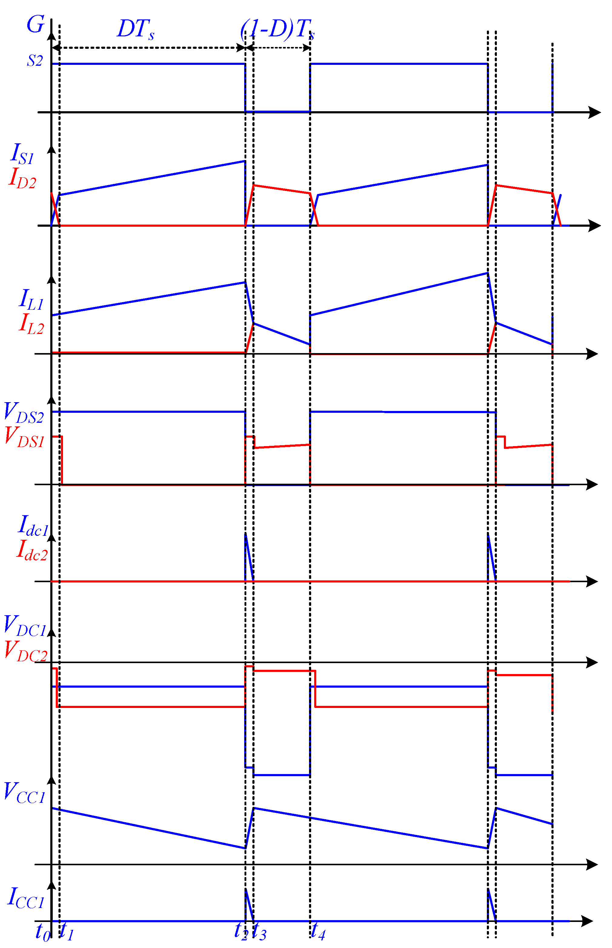
Figure 4 illustrates the characteristic waveforms of the CCCI-BDC converter boost mode operation. The gate pulses of switch (
Vg1) which triggers boost mode and gate pulses of switch (
Vg2) which triggers buck mode are complimentary. Let boost switch (
S1) and buck switch (
S2) duty cycles be assumed as
and
, respectively. Here, T represents the time period of switches
S1 and
S2. In the forward boost mode, switch (
S1) operates in pulse width modulated mode and diode
D2 operates in freewheeling mode. The boost mode operation is further classified into four operating modes in a switching period, and equivalent circuits of individual modes are illustrated in
Figure 5.
- A.
Mode-1 (t0 < t < t1): (S1 ON, D2 ON)
During this mode, switch
S1 is triggered to ON state and diode
D2 continues in conduction from the previous state. The switch
S1 enables linear charging of inductor
L1 and the inductor
L2 discharge path is through the load
RH. Clamped diodes
Dc1 and
Dc2 are in reverse bias, and the current through the inductor
L1 and
L2 is given by
The expression for voltage clamping diode (
Dc1) current and voltage clamping capacitor (
Cc1) voltage is given as
At the instant t = t1 the current through L1 and L2 is equal. Then, the diode D2 will be reverse biased and clamped diode Dc2 will become forward biased, because of the clamped capacitor Cc1.
- B.
Mode-2 (t1 < t < t2): (S1 ON, D2 OFF DC2 ON)
In this mode,
S1 is continuing the conduction from the previous state, so the current through
L1 (
) reaches its maximum value and the current
reaches zero. In this mode, the inductor
L2 leakage energy is freewheeled through
CC1 and
DC2. So, the diode
D2 will become reverse bias. Now, the current through
L1 and
L2 is
The voltage across the clamped diode
DC1 and current through the clamped capacitors are expressed as
- C.
Mode-3 (t2 < t < t3): (S1 OFF, D2 ON, DC1 ON)
This mode begins after
S1 is turned off at
t =
t2. So, the polarities of
L1 will change and at the same time both inductor
L1 and source together are ready to discharge. However, during this instant, the diode
D2 will come to forward bias. During this period, the stress due to leakage inductance on
S1 will divert through
Dc1. After that, the diode
D2 will become forward bias, and the voltage across the clamped capacitor and the input current is expressed as
where
- D.
Mode-4 (t3 < t < t4(T)): (S1 OFF, D2 ON, DC1 OFF)
In this mode,
S1 remains off and
D2 is in forward bias. The clamping diodes
Dc1 and
Dc2 are both in reverse bias. This mode begins at
t3 where current
is equal to
. In this duration (
t3–
t4), the inductor
L1 is completely discharged to the load. The magnetizing current reduces linearly while the coupled inductor supplies energy to the load. The absorbed energy in the coupled inductor is delivered through the route
VLV–
L1–
L2–D
2–
RH–
VLV. Therefore, the voltage across
L1 is expressed as
The current through the windings L1 and L2 is
- II.
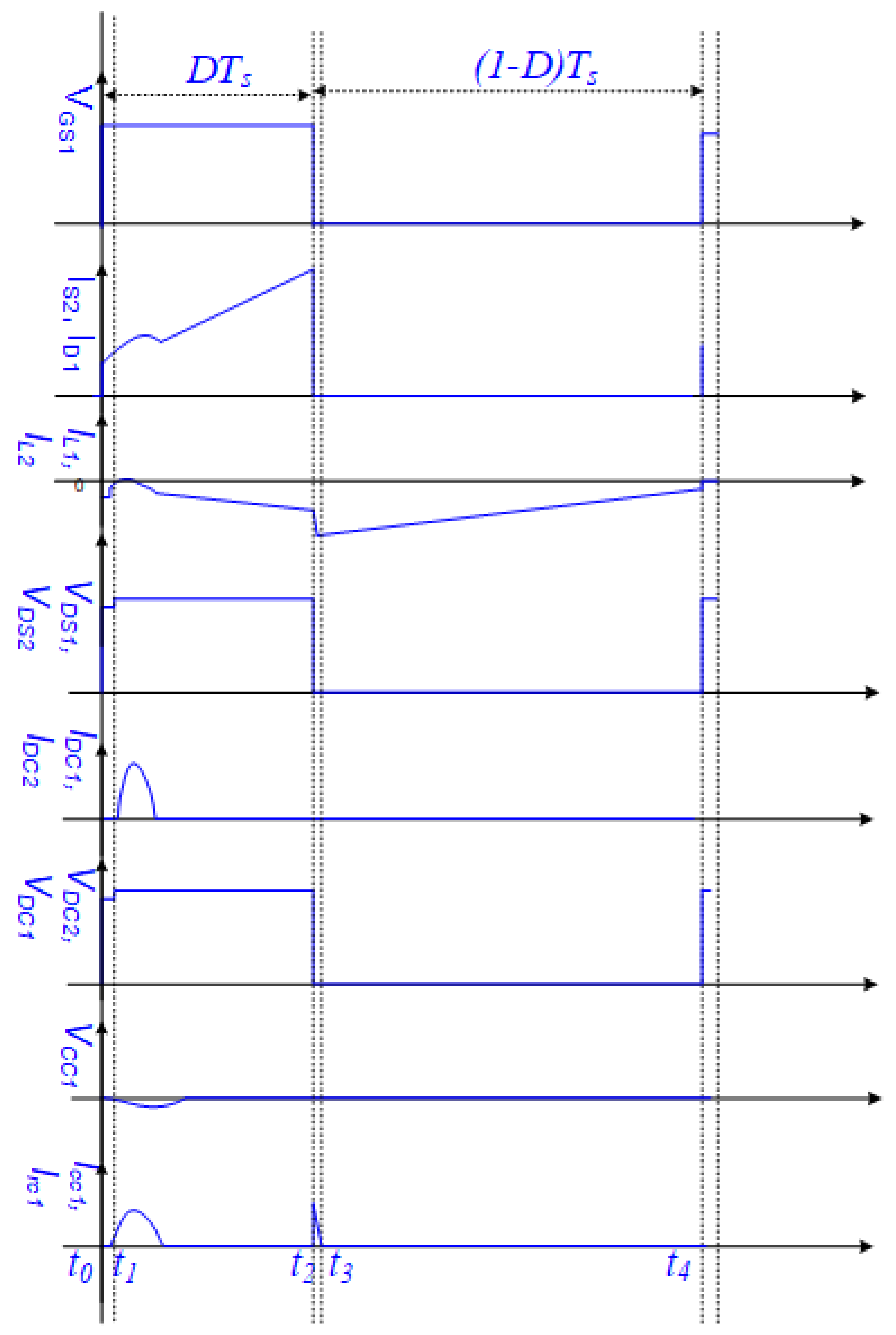
Buck Mode of Operation
The buck mode operation is further classified into four modes of operation (i.e., mode-5 to mode-8) across a switching period, and equivalent circuits of individual modes are illustrated in
Figure 6. Modes 5–8 are almost a repetition of Modes 1–4 in boost mode. This is reverse buck mode where switch (
S2) is operating in pulse modulated mode and the diode
D1 is operating in freewheeling mode. The magnetizing current (
iLM =
iL1) path runs from the DC bus, primary and secondary windings (
L1 and
L2) of the coupled inductor, and finally to the battery. The equivalent circuit for buck mode operation is shown in
Figure 6.
Figure 7 depicts idealized graphs of the converter operating in buck mode. Further division of modes is illustrated in
Figure 8.
- E.
Mode-5 (t0 < t < t1): (S2 ON, D1 ON)
In this mode, diode
D1 is already in conduction from the previous state and at instant
t0,
S2 gets triggered. The supply
VHV directly connected to inductor
L2 which is energized through
S2, while
L1 energy is discharged to load through
D1. The current through the CIs
L2 and
L1 increases and decreases linearly. At instant
t1, the current
is equal to
, and diode
D1 becomes reverse bias, so the polarities of
L1 are reversed. The clamping diode
Dc1 is in forward biasing mode and the leakage energy due to
L1 charges the capacitor
Cc1. The CI currents
and
are given as
- F.
Mode-6 (t1 < t < t2): (S2 ON, D1 OFF)
In this interval,
S2 is continuing its conduction up to
ton(=
t2) from the previous interval, and at instant t
1 the diode
D1 becomes reverse bias, as both the currents are equal. At this instant, the inductor
L1 changes its polarities. Thus, the clamped diode
Dc1 is in forward biasing mode and the leakage energy due to
L1, charges the capacitor
Cc1. The energy stored in
L2 discharges at load. The clamping diode current and voltage across
L1 and
Cc1 are expressed as:
- G.
Mode-7 (t2 < t < t3): (S2 OFF, DC2 ON, D1 ON)
During this interval, the switch
S2 and diode
Dc1 are triggered off, which will change the polarities of
L1 and
L2. Therefore, the diodes
D1 and
Dc2 are forward biased and the energy absorbed from
L1 freewheels through
D1. The leakage energy stored in
L2 is recovered by charging
Cc1 through
Dc2. During this period, the turn off voltage of
S2 due to the leakage inductance is reduced by the clamping circuit. The current through both the CIs is expressed as shown below:
By assuming the voltage ripple on
Cc1, the commutating voltage across
S2 is given as
- H.
Mode-8 (t3 < t < t4(=T)) (S2 OFF, DC2 OFF, D1 ON)
In this interval, the switch
S2 remains off. The current
is completely discharged and reaches zero, so the diode
Dc2 will get reverse bias and the current
freewheels through diode
D1 until the next cycle starts. The clamped diode
Dc1 is again forward biased due to clamped capacitor
Cc1. At instant
t =
t4, the switch
S2 again starts conduction and will repeat the cycle. During this mode, the current through CIs are expressed as:
From the above equations, output and switch voltages can be calculated as
- III.
Selection of Voltage Clamping Circuits
The problem of voltage spikes during turn off of both the switches is resolved using the single voltage clamping circuit. The proposed voltage clamping RCD circuit contains a diode in parallel with the series connection of resistor and capacitor, not only clamping the spike in voltage during turn off, but also minimizing the leakage inductance of the coupled inductor. The corresponding graphs of boost mode and buck mode of the circuits discussed above are illustrated in
Figure 5 and
Figure 8. For the right choice of these clamping circuit component (clamping capacitors and resistance) values, after the design, several iterations of MATLAB/Simulink based simulations were carried out. The
IDc1 and
IDC2 (current through RCD snubber circuit diodes
DC1 or
DC2) present less pulse width. Therefore,
Dc1 and
DC2 are of smaller rating as compared with conventional solutions. For hardware validation, the values of
CC1 and
CC2 are obtained from (15). The proposed single voltage clamping circuit has the advantages of less component count, simple structure, size reduction, and cost reduction.
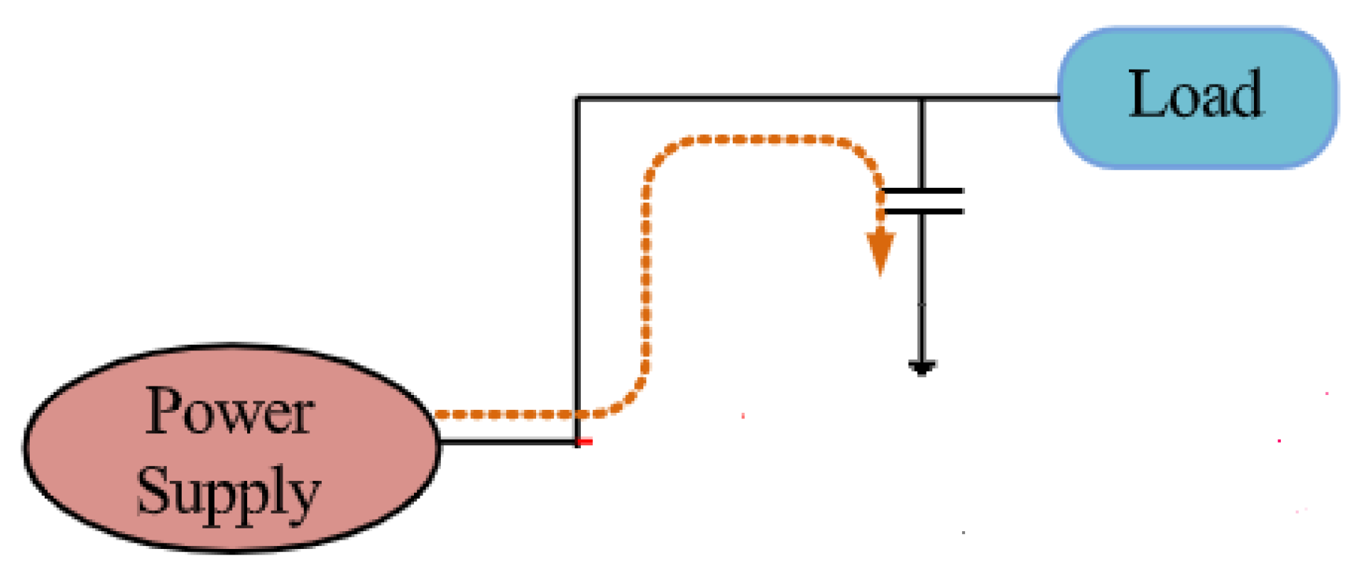
The instant a device is triggered on; a maximum instantaneous flow of current occurs through the device due to the initially uncharged energy storage elements. This peak current is called inrush current. Inrush current is far greater than the steady state current. The reason for the occurrence of inrush current is the input capacitor, as shown in
Figure 9. Usually, capacitors are placed at the input of non-linear loads (power electronics converters) and those capacitors get charged up during the time when the device is powered on. If left uncontrolled, it will cross fewer times higher than its rating, even with nominal value. Inrush current is visible in the case of DC supply in proportion to the magnitude of voltage.
Figure 10 illustrates the current waveform when the device is powered ON. The shape of the waveform indicates a rising peak, decreasing gradually to reach the steady state value after a certain time. This transient current waveform is the inrush current. The inrush current seriously damages the input rectifier, power switching device, and fuse and reduces the reliability and lifetime of the system.
To investigate the inrush current profile in the proposed converter with the simulation parameters for the conversion of 24 V to 200 V, the changes in inrush current are observed in the input current with respect to changes in input voltage, load current, and duty ratio during starting.
- V.
Control-to-Source Current and Control-to-Output Transfer Function
Control-to-source current and control-to-output transfer functions are obtained by using the state space averaging technique, which can be given as
where
k1–
k10 are detailed in
Appendix A.
To establish the conclusion from the derived transfer functions, step responses for the load, line, and duty cycle variations are plotted as presented in
Figure 11.
From
Table 1, it is observed that, for the step response of input current to input voltage in the transfer function, there is a 37.5% reduction in inrush current as one compares conventional and proposed converters subjected to changes in line voltage. It is also observed that the inrush current of the proposed converter reduces by 9% of overshoot with respect to the conventional converter, when one measures the step response of the output voltage to the input voltage transfer function. Further, it is noted that there is a 6.8% reduction in inrush current between conventional and proposed converters, when there are load variations. Finally, one can see that the percentage reduction in inrush current is 10.71% with respect to the changes in duty ratio, comparing conventional and proposed converters. These responses show that, for the line and load variations, variations in the input current and output voltage are much less in the proposed converter with respect to the conventional converter.
3. Simulation Results and Discussion
The following are simulation studies of the single voltage clamping CCCI--BDC. Buck and boost modes have been implemented on the MATLAB/Simulink platform. Parameters considered for the simulations are given below in
Table 2.
For the purpose of highlighting the performance of the proposed CCCI--BDC, a single voltage clamping circuit has been employed to augment the capabilities, and it is denoted as Voltage Clamping CCCI--BDC (VCCCCI--BDC). The MATLAB/SIMULINK platform is used to obtain the simulation results of the proposed converter.
Table 2 details the design specifications of the CCCI--BDC converter during different modes of operation.
Figure 12,
Figure 13,
Figure 14 and
Figure 15 contain the waveforms of both CCCI--BDC and VCCCCI--BDC during steady state condition in both boost and buck modes, respectively.
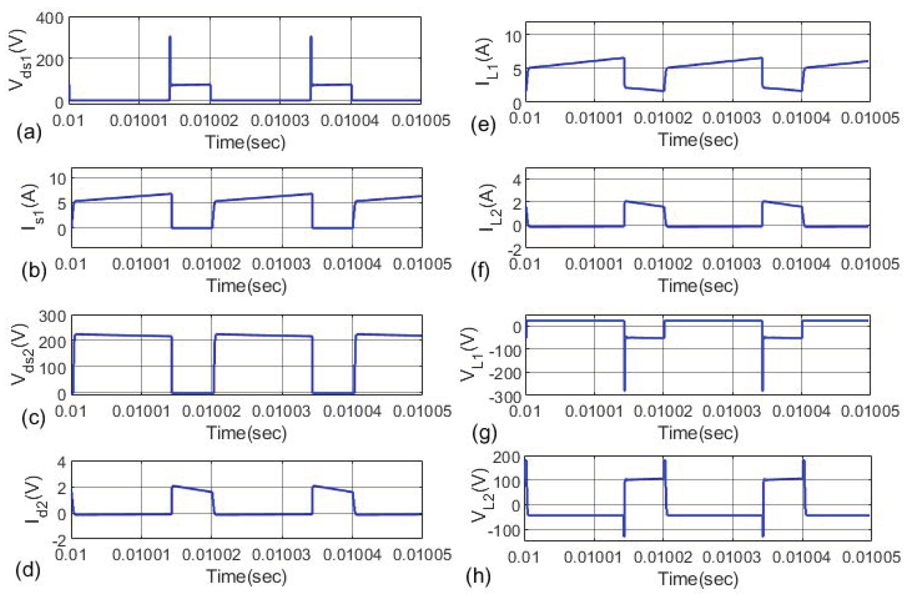
Figure 12a and
Figure 13a show the switch (
S1), voltage (
Vds1), and current (
Ids1) of CCCI--BDC and VCCCCI--BDC in boost mode while
Figure 13a and
Figure 14a show the switch (
S2), voltage (
Vds2), and current (
Ids2) of CCCI--BDC and VCCCCI--BDC in buck mode, respectively.
Simulation results of switch (
S1) voltage and current, switch (
S2) voltage, diode (
D2) current, and coupled inductor currents in both sides (primary and secondary), as well as the coupled inductor primary voltage and secondary voltage during discharging (boost) mode of CCCI--BDC operation are presented in
Figure 12a–h, respectively. Similar results have been captured during discharging (boost) mode of VCCCCI--BDC for the purpose of comparative analysis and presented in
Figure 13a–h, respectively.
From these results, it can be noted that stresses on the main device (
S1) during discharging (boost) mode are significantly reduced. A similar kind of analysis is carried out for the charging (buck) mode of CCCI--BDC and presented in
Figure 14. Simulation results of voltage and current at switch (
S2), switch (
S1), diode (
D1), as well as the primary and secondary currents and voltages in the coupled inductor, during charging (buck) mode of CCCI--BDC operation, are presented in
Figure 14a–h, respectively. Similar results have been captured during charging (buck) mode of VCCCCI--BDC for the purpose of comparative analysis and presented in
Figure 15a–h, respectively. From these results, it can be noted that stresses on the main device (
S2) during charging (buck) mode are significantly reduced.
The observation from
Figure 12a and
Figure 13a are that
Vds1 is 312 V in CCCI--BDC and it is 96 V in VCCC--CI BDC. Further, the observation from
Figure 14a and
Figure 15a are that
Vds2 of
S2 is 608 V in CCCI--BDC and it is 240 V in VCCCCI--BDC.
Figure 12a and
Figure 13a show the value of reduced switching spike of
Vds1 in
S1. Figure 14a and
Figure 15a show the corresponding reduction in switching spike of
Vds2 in
S2.
Figure 13d and
Figure 15d show that buck and boost modes are realized.
Figure 16A,B illustrate the bidirectional operation of the converter, with 200 V as high voltage and 24 V as low voltage. The voltage ripple is also within the limits of 1% as is evident from
Figure 16, for both buck mode and boost mode.
4. Hardware Results and Discussion
The proposed CCCI-BDC has been verified by experimental investigation in both modes of operation, i.e., boost and buck modes. For the experimental validations, a laboratory scale prototype was developed, as illustrated in
Figure 17. It primarily comprises of two IRFP 250 N MOSFETs driven by optically separated TLP250 driver circuits, one EZPE50506MTA capacitor, and one coupled inductor. A TELCON-25-based current sensor and AD202JN-based isolation amplifier sense the inductor current and capacitor voltage, respectively. As shown in
Figure 17, sensed quantities are processed by a signal conditioning circuit to control these state variables (i.e., inductor current and capacitor voltage). The corresponding values of different device specifications and variables used for such an investigation are mentioned in
Table 3. The suggested CCCI-BDC was proven to satisfactorily operate in boost and buck modes during experimental investigation, the setup of which is shown in
Figure 17. The CCCI-BDC hardware prototype was built with the help of SiC MOSFETs and an FPGA controller, illustrated in
Figure 17. Two lamps of 12 V and 50 W rating were used as a load for this test setup. The system parameters are validated for steady state and transient modes.
The input voltage levels are 12 V and 24 V. The corresponding graphs of device voltages, input current, load current, and capacitor voltages are extracted for both conventional as well as proposed converters. Their performances have been compared experimentally. The conventional converter necessitates two capacitors (one CHV for boost mode and another CLV for buck mode respectively), but in the proposed converter, only one capacitor (CC) supports both modes of operation, thus acting as an equivalent for both capacitors in the conventional system.
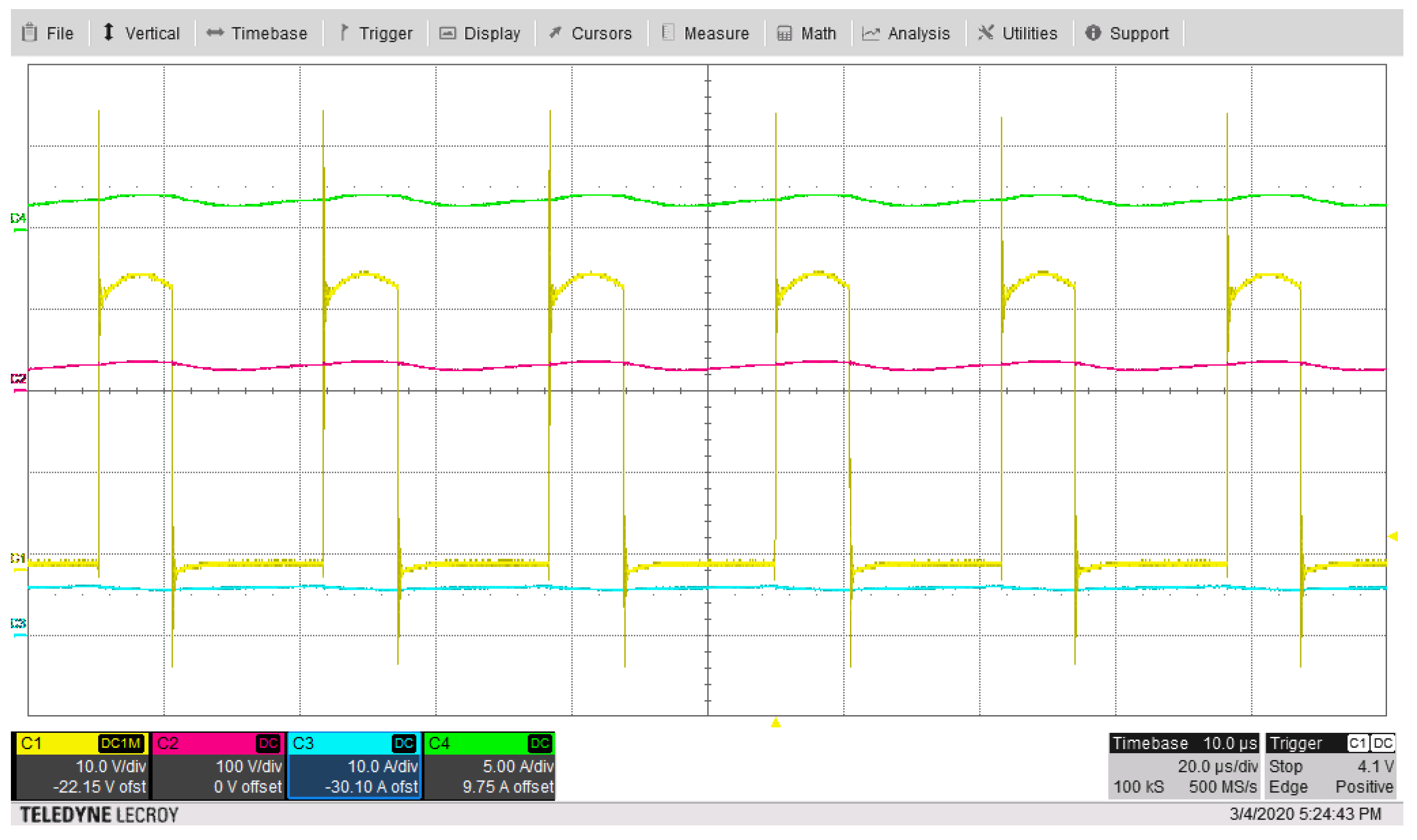
The input current, load current, and capacitor voltage corresponding to gate pulses are recorded herein in
Figure 18. A first observation regarding input current peak shows 8.57 A in the traditional converter but 8.27 A in the proposed converter for similar load current values. Similarly, the capacitor voltages for the traditional converter and proposed converter are 23.2 V and 12.1 V, respectively (a reduction of 46.25%).
For real time performance validation, various features of a vehicle, e.g., faster load turn off, smooth turn on, and converter switching ON and OFF with different duty cycle variations, are simulated. The various capacitor voltages, input currents, and load currents are measured for these features to be obtained. A closer look at the variation of maximum values of these signals during ON and OFF are illustrated here in
Table 4.
It can be inferred from
Table 5 that the proposed converter outperforms the conventional converter during steady state conditions, in terms of input current and capacitor voltage ripple values.
The microscopic view of input current, capacitor voltage, and load currents was obtained for the purpose of analyzing the ripple content. The findings are reported in
Table 5. This clearly shows the capacitor voltage in proposed converter is 3.33% less with regard to the conventional converter. Similarly, the input current is 2.4% less for similar load current ripples. The graphs of the current in the inductor, voltage in capacitor, current in load, and gate pulse for the top switch were obtained for four switching cycles, in the reverse buck mode of operation. The following observations have been made from these readings. Firstly, the maximum value of input current is 9.02 A for the CCCI-BDC converter but 8.8 A for the corresponding input current in the traditional converter. Likewise, the capacitor voltage in the proposed converter is 12.6 V, but the capacitor voltage for the traditional converter is 24.8 V, equivalent to a 50.8% reduction.
The various capacitor voltages, input currents, and load currents measured for these features in buck mode were obtained and are presented in
Figure 19. The performance of the converter was checked for various criteria, such as smooth startup, quick load turn off, and turning the converter on and off under different duty cycle values. This was estimated using the values of input current, capacitor voltage, and load current. Detailed analyses of the maximum values of these parameters during steady state condition have been performed and the results are tabulated in
Table 6. It can be inferred from
Table 6 that the proposed converter demonstrates better performance than the conventional converter not only during steady state conditions.
Table 7 demonstrates the superior performance of the proposed converter in terms of capacitor voltage stress, during both steady state ripples. From
Table 7, the ripple content can be compared in terms of input current, capacitor voltage, and load current, for the conventional and proposed converter, after observing a microscopic view of the same. The ripple content in capacitor voltage is 3.33% less in proposed converter vis–a-vis the conventional converter, for the same load current.
Efficiency:
This paper considers the parasitic resistance of inductors and capacitors, as well as the diode forward conduction losses, to compute the efficiency analysis of the inverter. In all topologies, the parasitic resistances of the inductor and capacitor are and , respectively, and the forward conduction loss of the diode due to forward voltage () is assumed to be the same. This manuscript also considers the effect of parasitic resistances and the forward voltage drop of main power devices (MOSFETs).
The calculation of losses and efficiencies of CCCI-BDC and CI-BDC was carried out by considering the equivalent circuit with various parasitic components and the relevant formulas are shown in
Table 8.
Figure 20 depicts the losses incurred in various components of the CCCI-BDC in relation to the duty ratio, which is calculated using the aforementioned formulas. According to these findings, at lower duty ratios, the diode is the main source of losses among all other components of the converter. MOSFETs, on the other hand, cause more losses at higher duty ratios. Capacitor losses are lower when compared to other components. The proposed converter’s efficiency is 93.8% at the rated values, as shown in
Table 3. In similar way, CI-BDC efficiency calculation is also carried out and found to be 93.2%. Hence, it can be understood that the proposed converter not only reduces ripples as well as the stresses on capacitors and devices, but also improves efficiency.


 ,
, 


