1. Introduction
In the field of microelectronics, Process Design Kits (PDKs) serve as a starting point for integrated circuit design, acting as a bridge between design engineers and manufacturing companies [
1]. During the chip design process, the foundry provides specific data and script files in the Electronic Design Automation (EDA) tool, as the PDK library used by the designer contains details about the semiconductor process. This enables design engineers to quickly create chips using the PDK [
2]. A PDK typically consists of symbols, the Component Description Format (CDF), parameterized cells (PCells), the SPICE simulation model, the physical verification rule file (PVRule), and other components [
3].
A PCell is a programmable unit that allows users to modify parameters and create different PCell instances [
4]. In mainstream Electronic Design Automation (EDA) simulation software, although there are rich UI interactive interfaces, circuit schematic diagrams are typically stored in the background folder of simulation software as netlist files when engineers perform front-end simulation [
5]. During back-end simulation, engineers need to manually splice device PCells and fine-tune the size parameters of PCells to obtain a circuit layout that closely matches the front-end simulation results, a process known as layout design.
As a critical part of the integrated circuit design process, layout design serves as a bridge that connects design and manufacturing. It involves performing layout and physical verification based on the netlist produced in the front-end design stage and generating GDSII data for manufacturing [
6]. While layout and routing are essential processes in layout design, they can be repetitive and tedious tasks. Therefore, automating layout and routing generation using computers to reduce the workload of engineers has become a classic problem [
7].
In the past decade, with the continuous development of semiconductor technology, Electronic Design Automation (EDA) has played an important role in circuit design, and in order to meet the growing market demand, the importance of computer-aided circuit design in the field of circuit design has continued to increase [
8]. In the field of digital circuits, algorithms can be used to generate structured Verilog format combinational circuits. The method is to store the calculated parameters in a structured form and use software to generate combinational circuit data sets. This method can be used with limited information, based on research on the reliability prediction of combinational circuits [
9]. Cindy et al. describe a random circuit generator used in FPGA architecture research [
10]. The generated circuits form a hierarchy of interconnected modules. At each hierarchy level, the modules can be connected in a bus, star, or dataflow configuration. The generated circuits can be used to create a baseline circuit and are more efficient than previous generators. The resulting circuits yield more realistic architectural conclusions.
With the development of machine learning technology, layout design performed by artificial intelligence-assisted engineers has begun to develop. In the work by Azalia et al. [
11,
12], chip placement is treated as a reinforcement learning problem by training an agent to place the nodes of a chip network list onto a chip canvas, designing a neural architecture to predict the rewards of various network lists and their positions, and extending reinforcement learning (RL) strategies to unseen regions using transfer learning. The goal is minimizing the PPA (power, performance, and area), reducing human engineers’ work from weeks to less than 6 h.
As the number of logic devices increases, the layout problem becomes more complex and is no longer limited to component sorting but also involves selecting suitable paths for each signal line. Thus, each signal line requires an appropriate wiring path in the second type of layout algorithm. Therefore, these types of layout algorithms typically involve a two-stage optimization process. The first stage is global optimization, which mainly focuses on component placement, while the second stage is local optimization, which mainly focuses on signal routing. Global optimization algorithms mainly use traditional heuristic algorithms, such as simulated annealing, genetic algorithms, and ant colony algorithms, to obtain an initial solution for the layout. Local optimization algorithms mainly use iterative improvement methods, such as Steiner tree algorithms, to optimize the routing of the signal lines based on the initial layout. Compared with the first type of algorithm, the second type of algorithm can obtain more accurate results, but it requires more computational resources and a longer optimization time [
13].
This aggregation of functional modules in each part also facilitates the optimization of the circuit layout. Various optimization algorithms, such as the genetic algorithm, particle swarm optimization, simulated annealing, etc., can be used to optimize the layout of each part; then, the optimized layout can be merged to obtain the final layout of the entire circuit [
14]. However, the problem of interconnecting optimization among different parts of the circuit still needs to be solved. The resulting global optimal layout may not be the optimal solution for each individual part. Therefore, further optimization is needed to balance the optimization of the entire circuit and the optimization of each individual part. In addition, with the continuous development of various materials, technologies, processes, and revised design rules, the layout and wiring optimization problem of VLSI circuits is still a challenging research topic.
There are numerous studies in academia on placement and routing algorithms for large-scale circuits, but there is a lack of research on placement and routing algorithms for small- and medium-sized integrated circuits. In the field of radio frequency (RF) circuits, mainstream simulators such as ADS provide relatively rough algorithms for compound process layouts. When the circuit structure becomes complex, it is common for device layouts to intersect. Therefore, engineers need to consider issues such as impedance matching and electromagnetic simulation when laying out the RF circuit. In other words, the distribution of metal connections among devices also impacts the final circuit performance of RF circuits.
M. Aktuna et al. [
15] developed a device-level early floor-planning algorithm for RF circuits based on the genetic algorithm (GA) aiming to optimize the physical layout of individual components or devices in RF circuits as early as possible in the design phase. The algorithm takes into account key factors such as device placement, routing, and performance metric optimization, including noise, linearity, power consumption, and impedance matching, and can dynamically adjust the size of the floor plan when necessary. It assists designers in identifying optimal floor plans, potentially reducing design iterations, and speeding up the time to market of RF circuits.
This paper discusses a layout stitching method for medium-sized analog circuits that is different from traditional layout algorithms. The method is specifically designed for generating radio frequency layouts in circuit design and reverse engineering fields. Given circuit topology and device dimensions, the proposed method places PCells (parameterized cells) to generate an initial RF layout, which can be mapped into ADS simulation software using scripts. In this description, the physical position of the PCell is determined by three factors: placement coordinates, rotation angles, and mirror reflections. By analyzing the input netlist file, the method determines the optimal combinations of these three factors. Specifically, a specific size vector is established based on the PCell structure of each device, and a decision function is established for each port to ensure that the PCell meets the design requirements after rotation and reflection operations. The approach was implemented on the C++ platform and tested using various possible stitching methods to achieve optimized layout stitching results. The final result is organized and automatic layout generation based on circuit logic that outperforms the relevant modules in ADS (Advanced Design System) in terms of performance.
2. Overview of Layout Splicing Methods
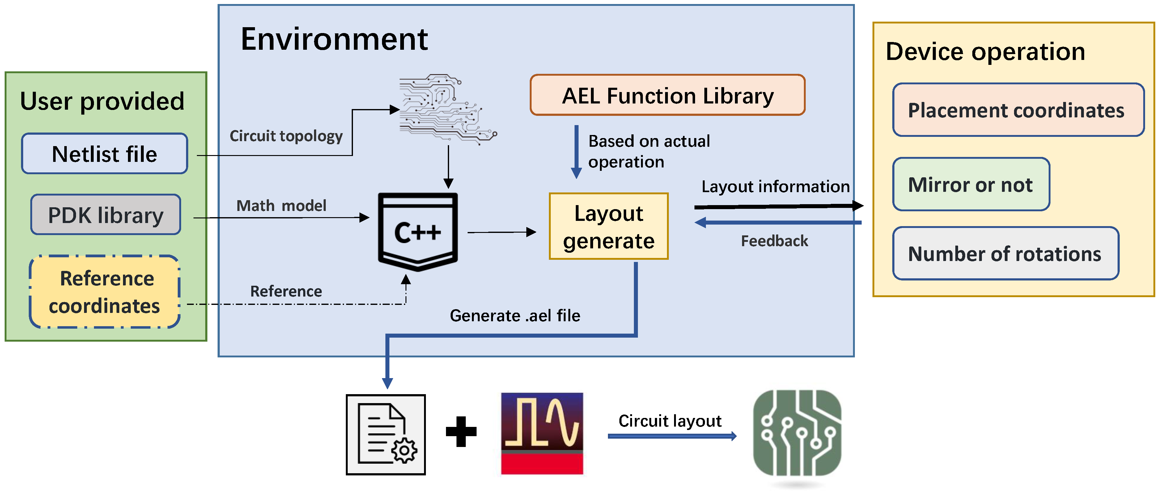
This paper describes a C++-based system developed to automate layout generation, as illustrated in
Figure 1. The system can be useful in both the field of back-end design and reverse engineering, reducing the repetitive work of RF circuit engineers in layout design [
16]. The system generates placement information of devices in the best possible layout combination based on the user-provided netlist file and PDK information. The placement information is combined with the self-developed AEL function library to output AEL files that can be recognized by ADS. By calling the AEL files in ADS, the system can automatically generate circuit layouts in ADS [
17]. The system effectively streamlines the layout design process and increases design efficiency while minimizing human error in the layout process. It can be a valuable tool for engineers facing time and resource constraints in the design process.
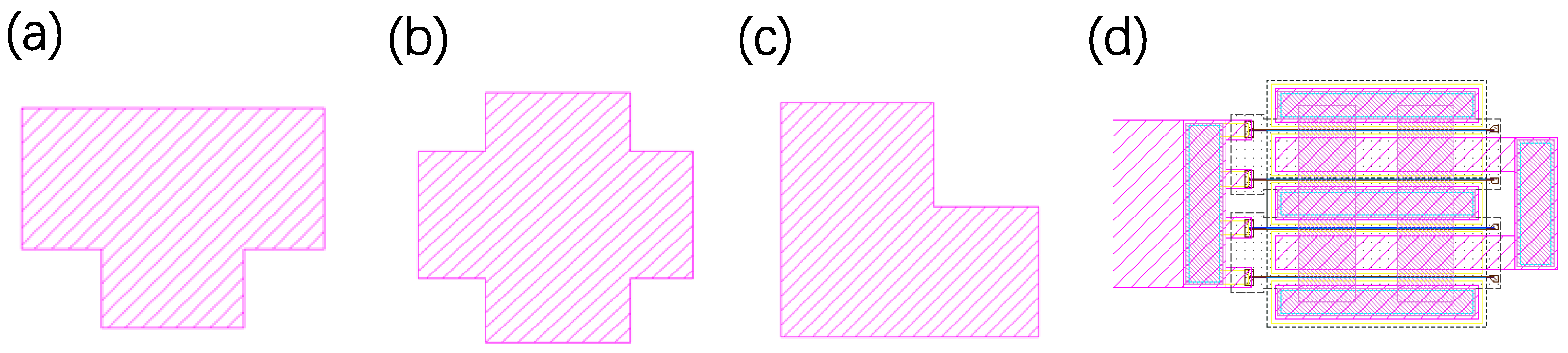
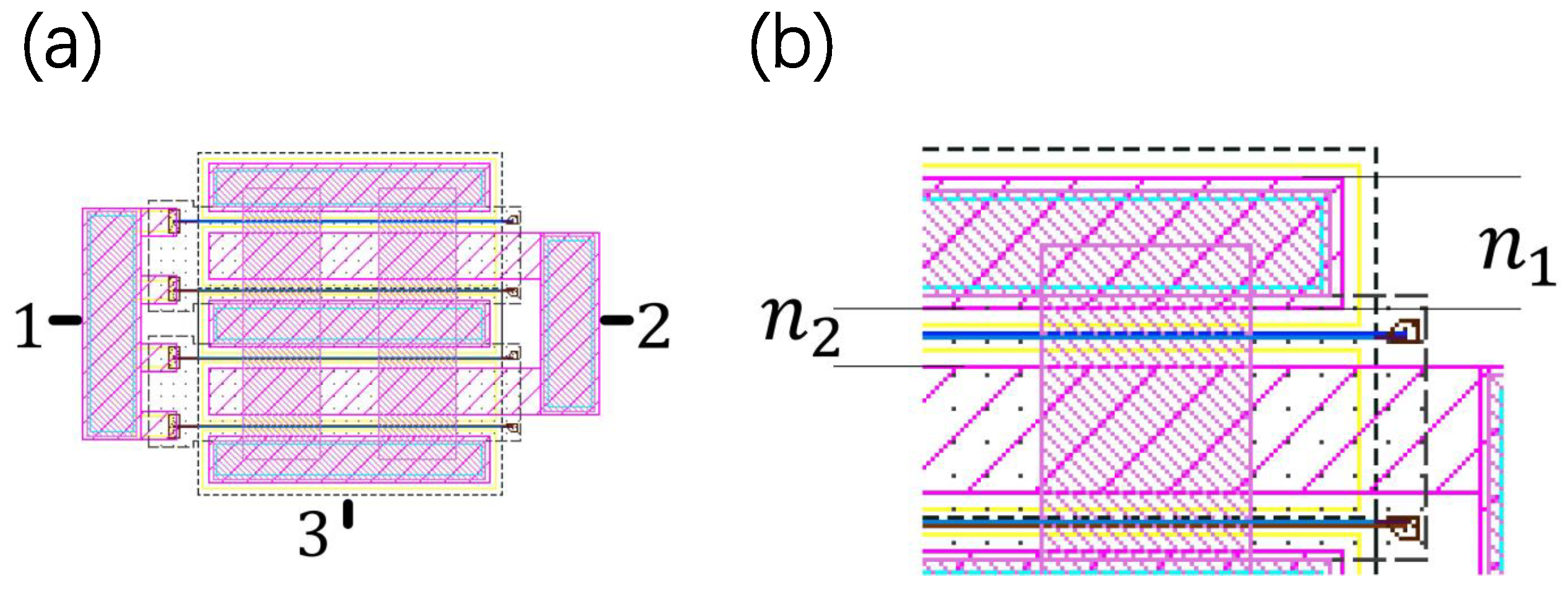
In the device PCell-splicing process, the circuit logic is known, and the length of the wire cannot be changed [
18]. To solve the problem of device intersection, mirror inversion of the asymmetric structure can eliminate the overlap under a certain probability phenomenon [
19]. Devices that can resolve the local overlapping of layouts with mirror inversion are referred to as traceable devices in this paper. The candidate devices for backtracking points include T-junctions, cross junctions, bends, and transistors. The structures of various traceable devices are shown in
Figure 2.
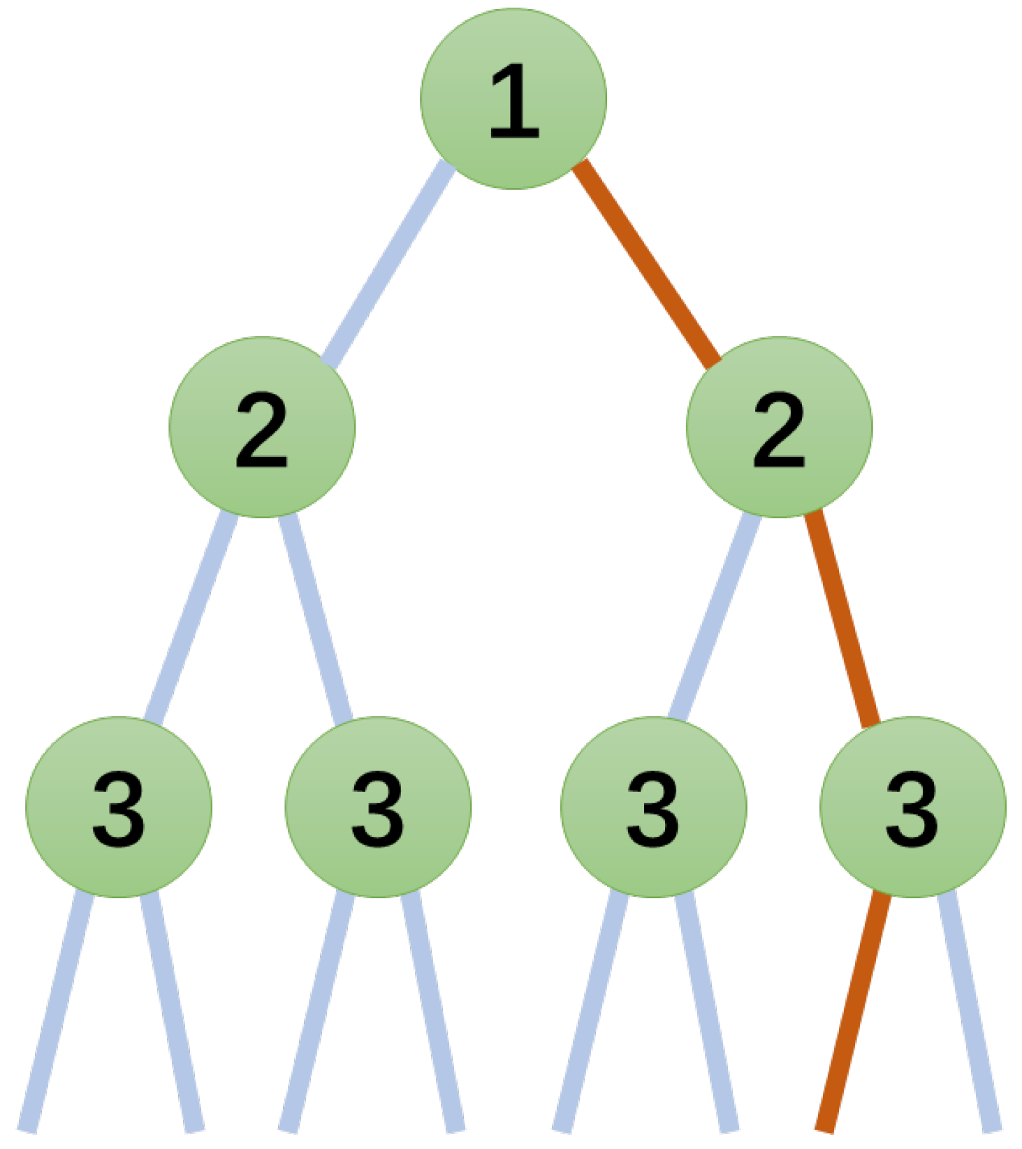
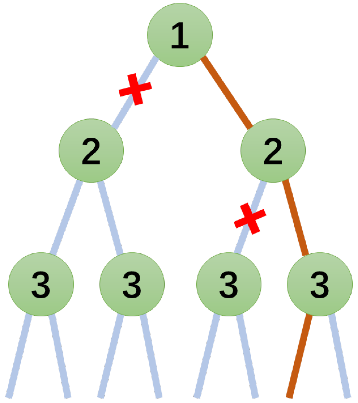
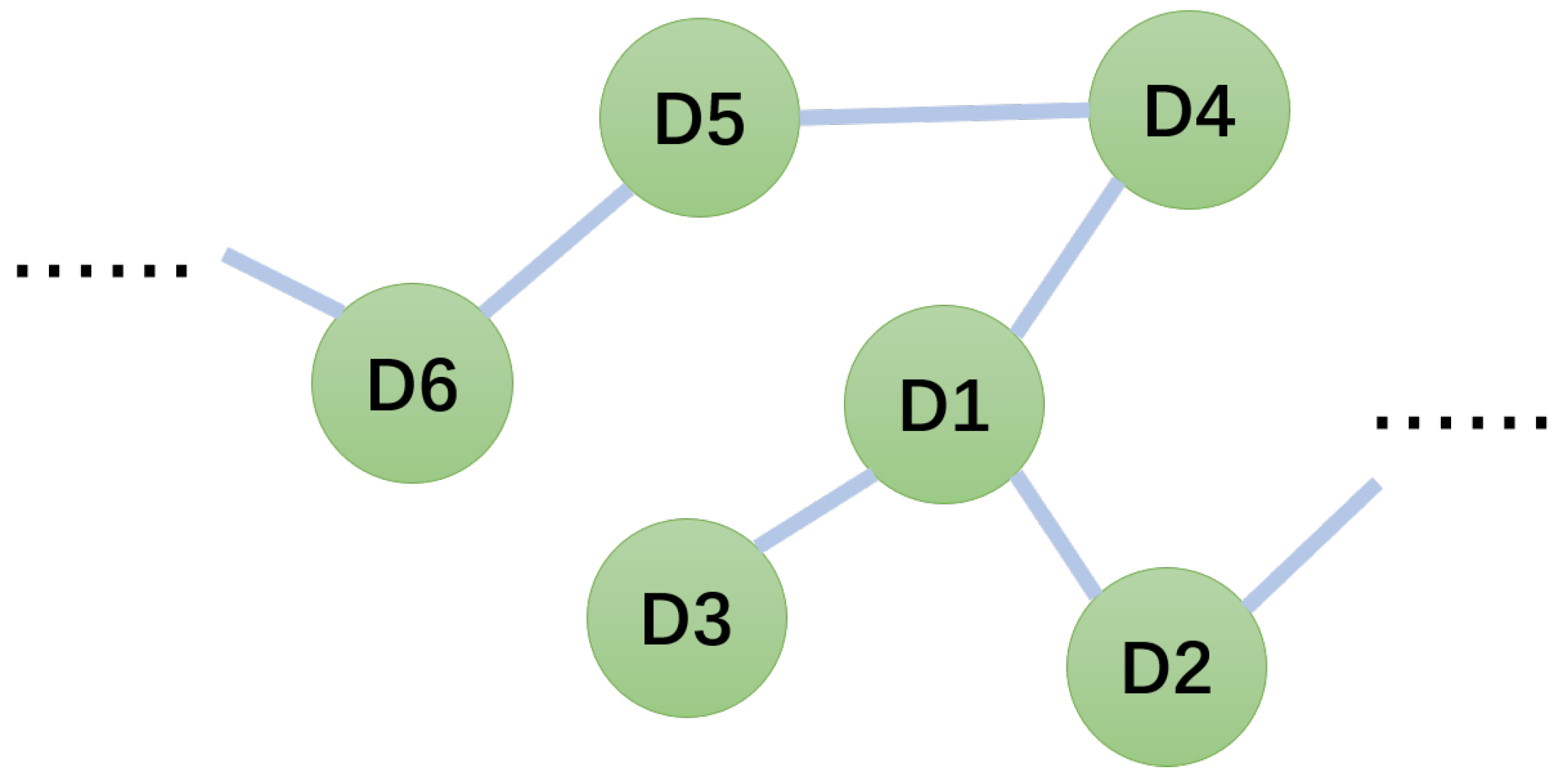
In this paper, a decision tree is used to model the layout stitching problem, as shown in
Figure 3. The number of the nodes represent the traceable device IDs that can be found on record. These nodes are referred to as “backtracking points” in this paper.
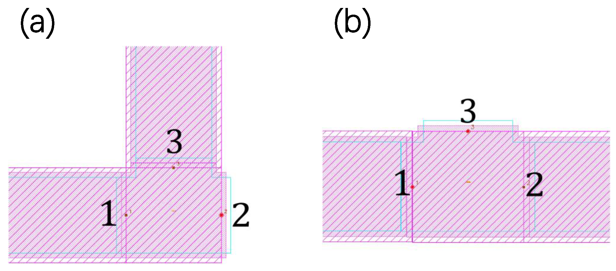
Using Node 1 as an example, the left subtree of Node 1 represents the concatenation of traceable device No. 1 without flipping, while the right subtree represents the mirror-flipped version of traceable device No. 1. As shown in
Figure 4a, when traceable device No. 1 is properly interconnected, a layout overlap occurs. To resolve this issue, a vertical flip operation can be applied to the first retrievable device, as demonstrated in
Figure 4b. Therefore, the state of layout stitching can be described by the splicing states at each backtracking point. By finding the correct path in the decision tree, the layout stitching problem of the RF circuit can be solved.
In this paper, the combination of the DFS (depth-first search) algorithm and the backtracking algorithm is used to traverse the decision tree [
20]. The DFS algorithm is a graph algorithm that starts from a vertex and explores as far as possible along each branch before backtracking. The basic process of browsing the tree structure based on the DFS algorithm is as follows: starting from vertex v, explore the unvisited adjacent nodes of node v until all nodes are visited [
21]. Based on this method, searching through the binary tree to find the correct solution has a time complexity of O(
), where n is the number of traceable devices [
22].
As shown in
Figure 5, to reduce the time complexity of the algorithm, this paper applies a combination of backtracking and topological features to “prune” the binary tree [
23]. Incorrect concatenation may result in overlapping layouts or unclosed loops. When device overlaps occur, the backtracking algorithm is used to return to the previous backtracking point and prune the left subtree of the node, until a correct concatenation path is found [
24]. Meanwhile, to ensure the normal concatenation of loop structures, the connection status of the devices that compose the corners of the loop can be determined, and the corresponding paths in the decision tree for this type of device can be directly selected to reduce the time complexity of the algorithm.
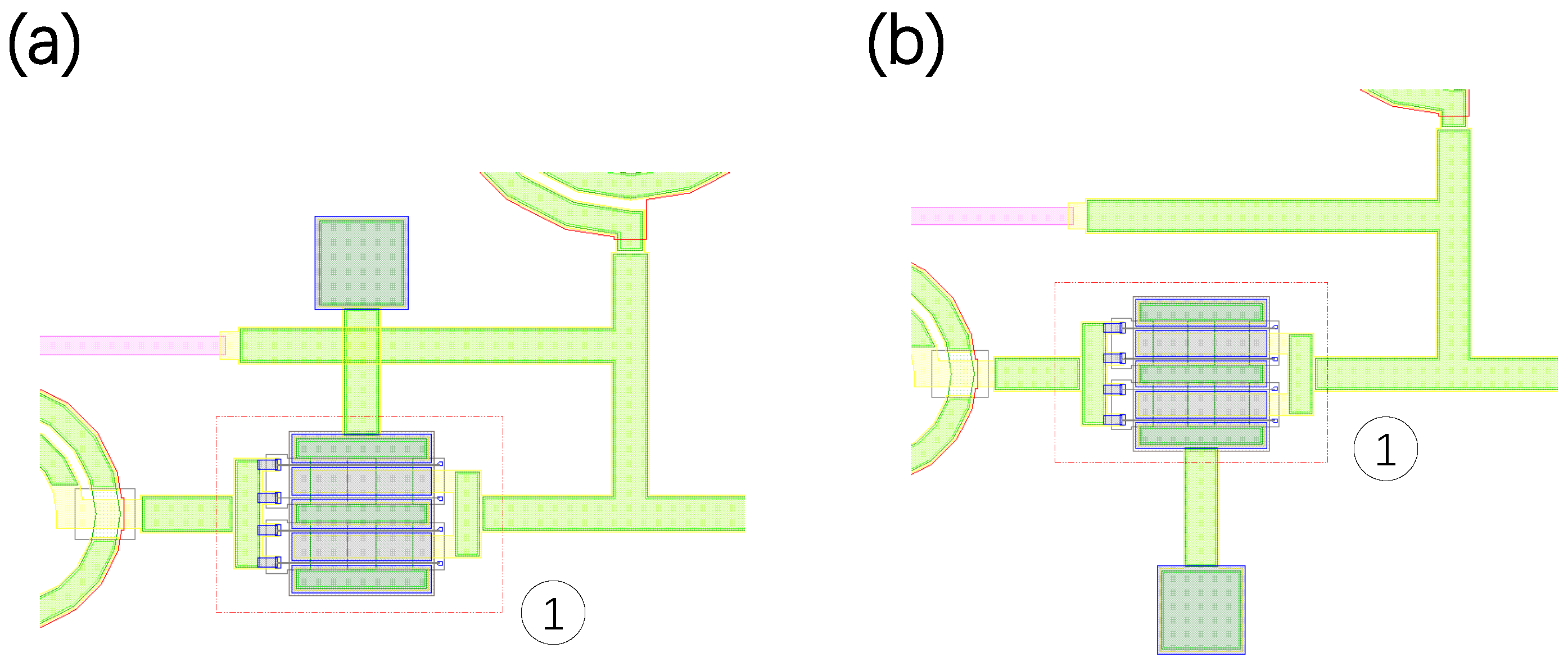
As illustrated in
Figure 6, Device 2 belongs to the retrievable device type and also composes the corner of the loop. During the layout concatenation process, when Device 2 is normally concatenated (as shown in
Figure 6a), an intersection occurs, and the loop structure fails to close properly. According to the topological characteristics of the RF circuit, whether Device 2 should be mirrored can be predetermined. Therefore, for the decision regarding Node 2, the correct path can be directly selected, resulting in the final successful concatenation illustrated in
Figure 6b. This operation realizes “pruning” and reduces the pathfinding time of the binary tree.
3. Device Addressing Model
In this chapter, a mathematical model is developed to describe the method for computing the coordinates of other pins based on the coordinates of pin 1 and the dimensional characteristics of the device to facilitate the description of the physical location of each device. The model takes the right direction as the positive x-axis and the downward direction as the positive y-axis. In the system designed in this paper, the physical coordinates of PCell placement are represented by the coordinates of pin 1. During the layout stitching process, it is necessary to consider the method of computing the coordinates of other pins after rotation and mirror operations.
3.1. Addressing Ports of Normally Placed Devices
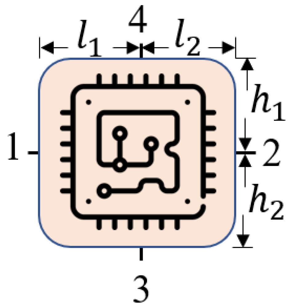
In the PCell structure involved in this article, there are at most four pins for each PCell on the RFIC device, and the shape of the RFIC device can be approximated by a rectangle. This means that the PCell structure of the device can be described by a rectangle and four boundary center points. Taking a four-port device as an example, its structure diagram is shown in
Figure 7. For a device with the coordinates of pin No. 1 being
, the device structure is described by size vector
X, and the calculation formula for size vector
X is
where
are the coordinates of port 1 of the device,
is the distance from port 4 to the left border,
is the distance from port 4 to the right border,
is the distance from port 2 to the upper border, and
is the distance from port 2 to the lower boundary.
For a four-port device whose port 1 coordinates are
, when the device is not rotated or mirrored, the calculation formula for other port coordinates is
where
are the port 2 coordinates,
are the port 3 coordinates, and
are the port 4 coordinates.
The device coordinates are represented by vector
P,
; then, (
2) can be organized into a matrix form:
where
and
X is the size vector of the device.
3.2. Addressing Ports after Rotation Operation
In this article, the term “rotation operation” refers to a 90° clockwise rotation of the device, using the coordinates of port 1 as the reference point. A schematic diagram illustrating the rotation of a rectangular device is shown in
Figure 8.
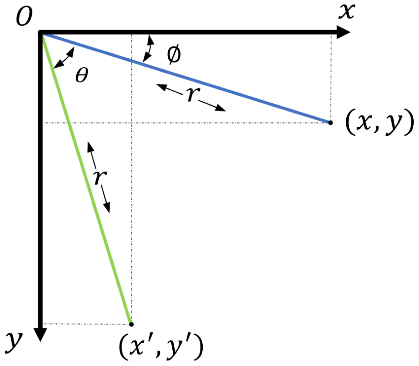
In the two-dimensional plane coordinate system, as illustrated in
Figure 9, the green line is the result of rotating the blue line,
, clockwise around the origin by an angle
. The endpoint of the green line is denoted as
, and the calculation formula for these rotated coordinates is
After rearranging Formula (
4), we can obtain
When the rotation base point is not the origin, the rotation process can be viewed as first translating the coordinates to make the rotation base point the origin [
25]. After the rotation is completed, the endpoint coordinates are corrected by translating them back to their original position [
26]. Following this principle, Formula (
5) can be corrected. For a point
with a rotation base point of
and an angle of rotation
, the resulting point is
. The coordinates
can be calculated as follows:
To summarize, for a device with port 1 coordinates
and port
i coordinates
, performing a 90° clockwise rotation operation with port 1 as the base point results in the new coordinates
, which are calculated using the following formula:
Formula (
7) is arranged with a matrix. For the device whose coordinate vector is
P, after n rotations, the calculation formula for its coordinate vector
is
where
.
3.3. Addressing Ports after Mirror Operation
In this paper, the term “mirror operation” refers to flipping the device vertically or horizontally with the coordinates of port 1 as the reference point.
Figure 10 illustrates four schematic diagrams of mirror flips for a rectangular device.
As shown in
Figure 10a,c, let
be the coordinates of port 1 of a device, and
be the coordinate of port i. When the device undergoes an up–down mirror operation (flipped upwards and downwards with port 1 as the reference point), the calculation formula for coordinates
of port
i is
As depicted in
Figure 10b,d, when a left–right mirror operation is applied to a device (i.e., the device is flipped horizontally with port 1 as the reference point), the formula for calculating coordinates
of port
i is
Let us arrange (
9) and (
10) in the form of a matrix. For a device whose coordinate vector is
P, after an up-and-down mirror operation, the calculation formula for its coordinate vector
is
where
.
After the device undergoes a left–right mirror operation, the calculation formula for coordinate vector
is
where
.
4. Dimension Vector for RFIC Device PCell in Compound Process
This chapter outlines the method for calculating the size vector of common RFIC components based on their size parameters provided in the netlist file. The PDK model used in this article was developed by WIN Company. However, due to the impact of the production process, the size vector obtained from the PCell size parameter needs to be numerically corrected [
27]. The discussed RFIC devices include circular inductors, capacitors, resistors, and transistors.
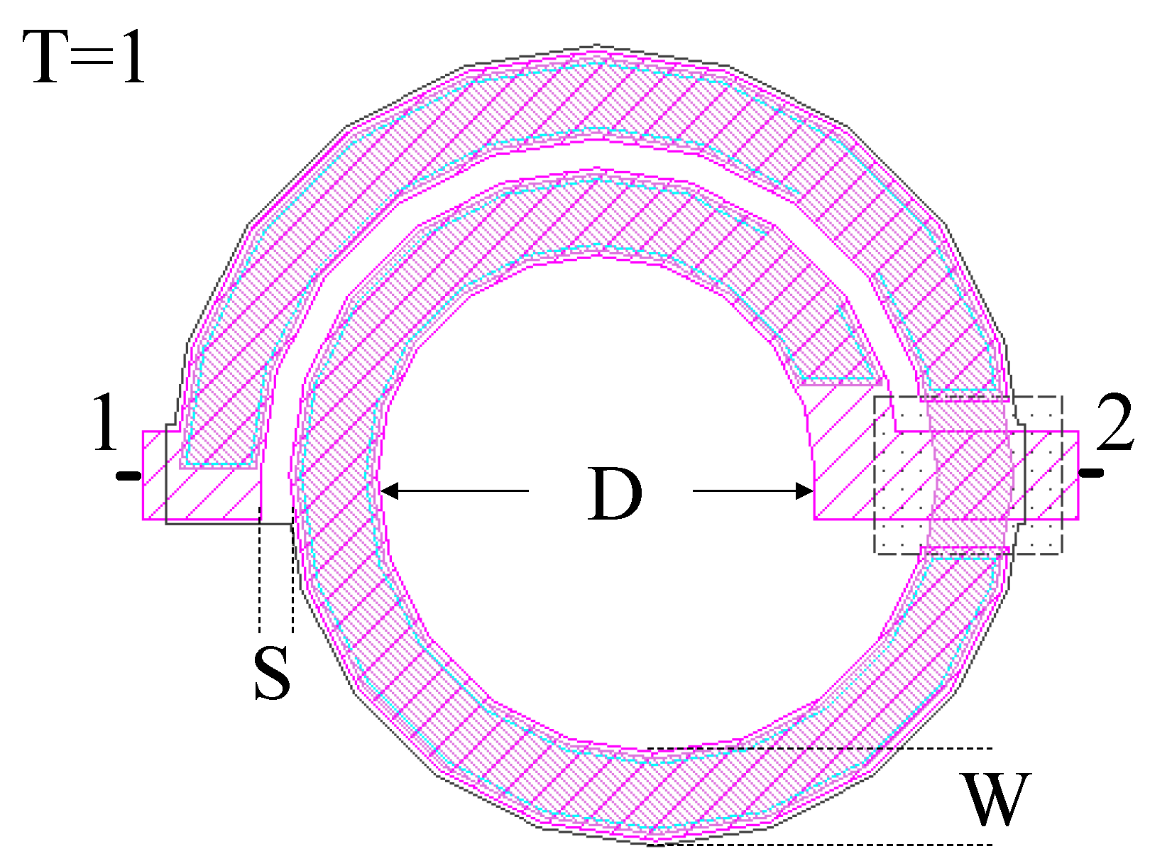
The size parameters for circular inductors include
W (line width),
S (line spacing),
D (inner radius), and
T (number of turns), as illustrated in
Figure 11. These parameters represent the physical characteristics of the inductor PCell structure.
When the size parameters are known, the calculation formula of the actual width between the two ports of the circular inductor PCell is
The formula for calculating the upper–lower width of the inductor is
In the former, is a correction parameter that is used to compensate for the difference between the theoretical length and the actual attempt. This parameter is only related to the device process.
To sum up, the calculation formula for size vector
of the circular inductor with port 1 coordinates
is
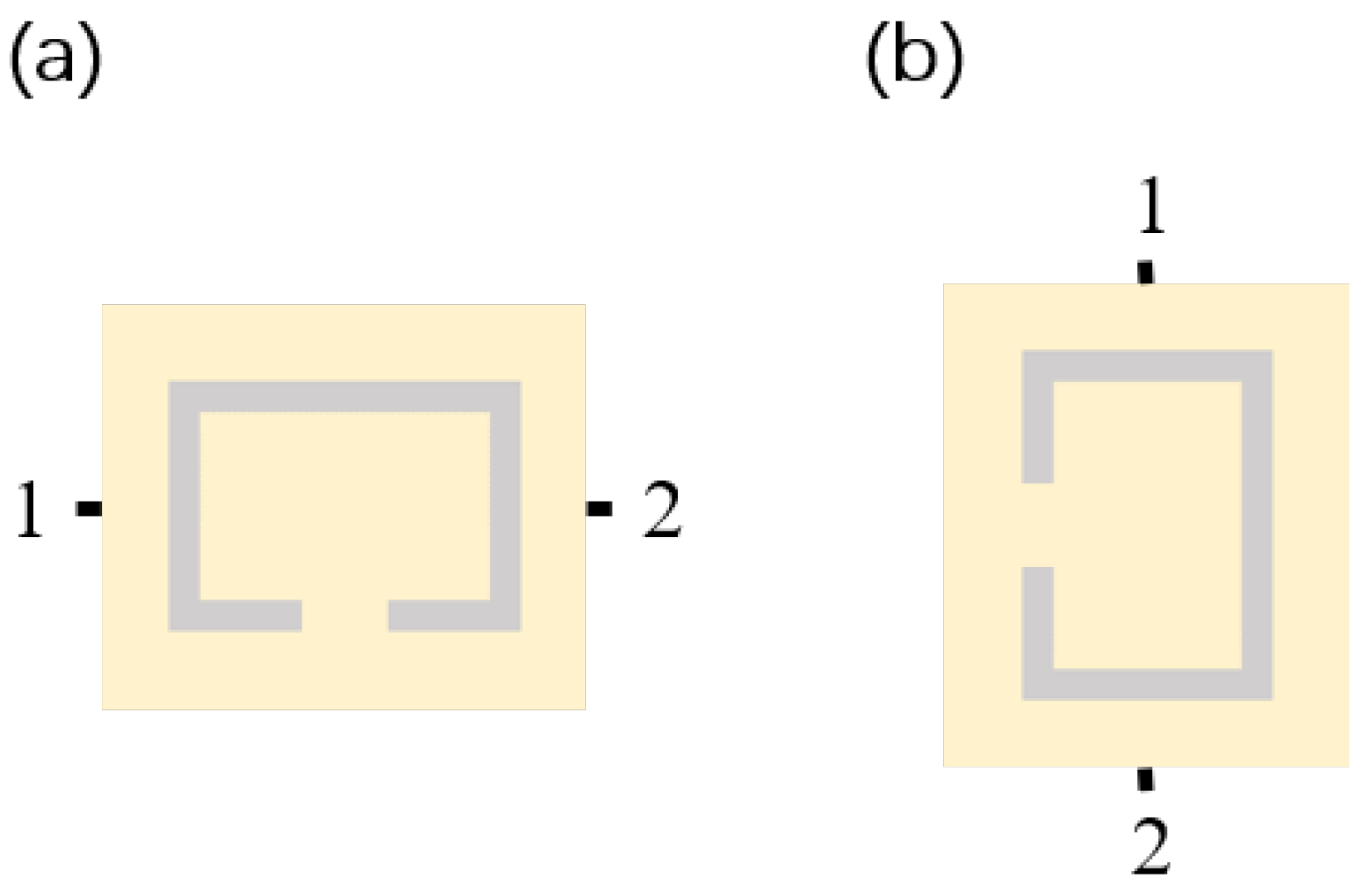
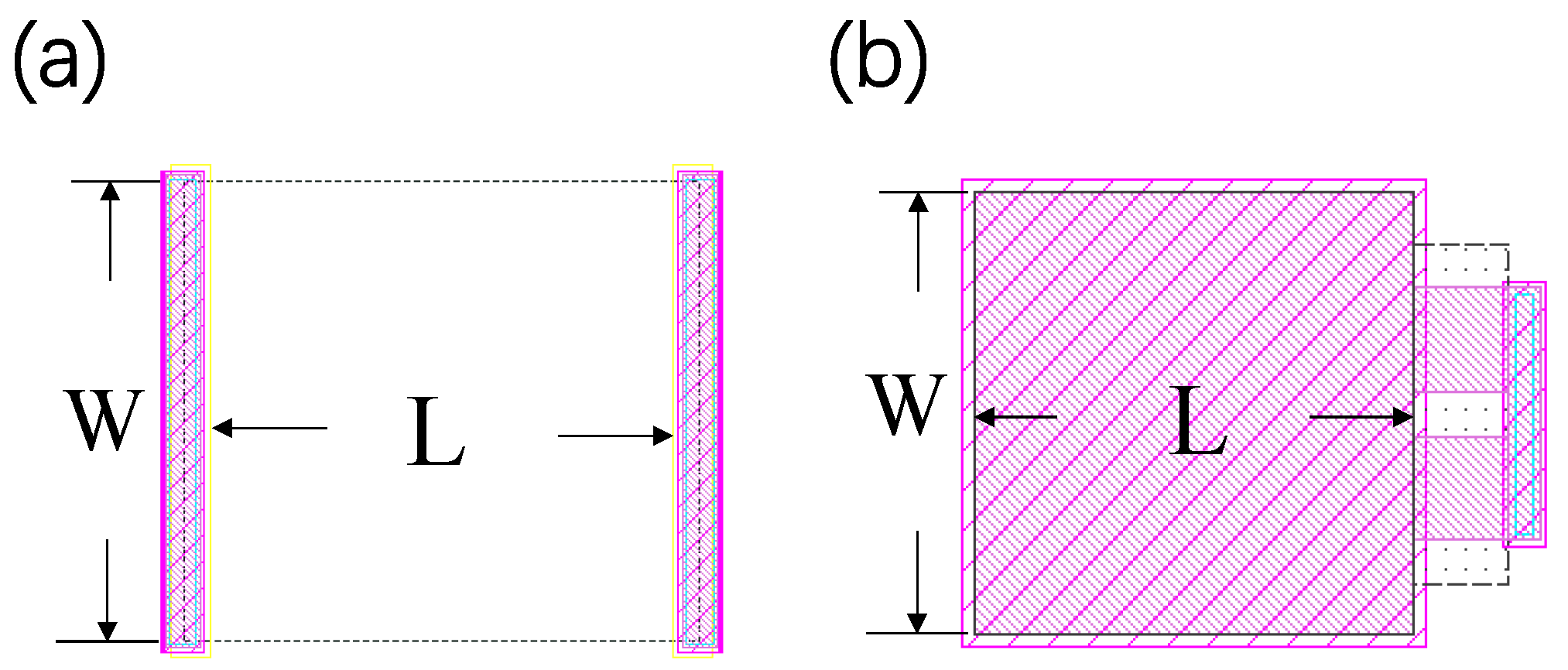
Resistors and capacitors have a rectangular shape, with the size parameters of resistors being
W (line width) and
L (line length). During the design process, a metal layer is used for connection at the resistor port, as shown in
Figure 12a. For capacitors, there is typically an air bridge at the two ports for connection, as shown in
Figure 12b.
The formula for calculating the actual width between the two ports of resistor and capacitor is
The formula for calculating the resistance width is
In the above, and are correction constants that have nothing to do with the size parameters.
The formula for calculating the capacitance width is
where
is the width correction parameter of the capacitor and
is the width of the air bridge.
To sum up, the calculation formula of size vector
of the resistor with port 1 coordinates
is
The calculation formula for size vector
of the capacitor whose port 1 coordinates are
is
The size parameters of a transistor include gate width (Ugw) and gate index (NOF). The PCell structure of the transistor is illustrated in
Figure 13.
In the horizontal direction, the length of the transistor is related to the size parameter in the following way:
Due to the asymmetrical structure of the transistor, the formula for calculating its length needs to be adjusted as follows:
where
and
.
In the vertical direction, the relationship between the width of the transistor and the size parameter is
where
is the width of the gate finger,
is the width of the gate finger gap, and
and
are the dimension correction constants.
To sum up, the size vector of the transistor is
where
are the port 1 coordinates of the transistor.
5. Layout Splicing Scheme
5.1. Strategies for Handling Ring Structures
After parsing the netlist file, an undirected graph is generated based on the PDK mechanism and the device connections described in the netlist [
28]. This is illustrated in
Figure 14. Unlike a traditional undirected graph, each node in this graph corresponds to a device in the netlist. It contains relevant information such as the device’s size and name, and the direction of its ports.
The minimum cycle structure of an undirected graph can be found using a depth-first search algorithm [
29]. In RF circuit layout, a Manhattan structure (horizontal or vertical) is commonly used for connecting metal [
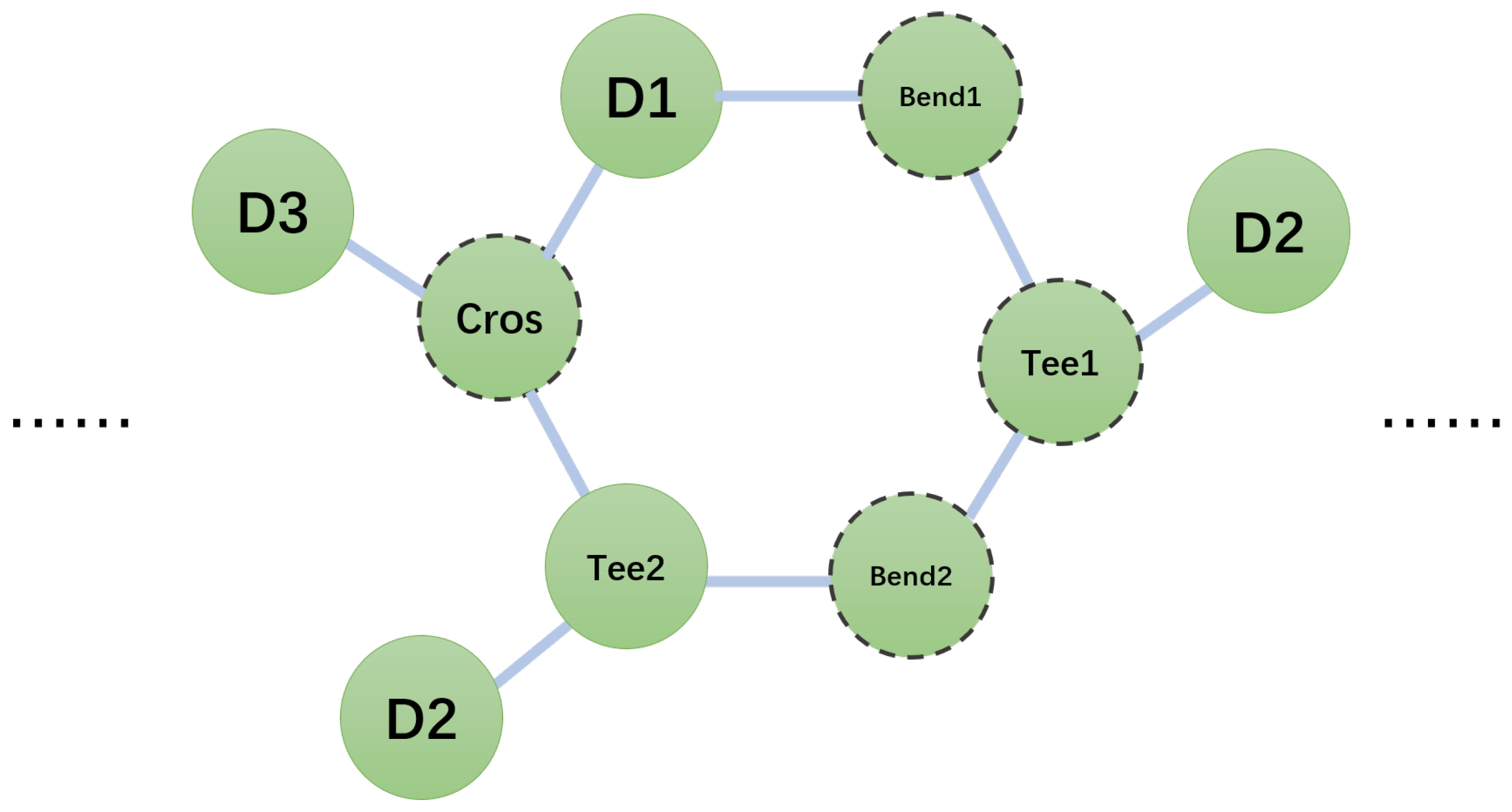
30]. Therefore, for a ring structure, as shown in
Figure 15, four corner devices are required to change direction when forming a ring. The devices marked by dotted lines, Cross, Tee1, Bend1, and Bend2, are the corner devices of the ring structure. During layout and routing, to ensure the proper closure of the ring structure, such corner devices cannot be considered routable devices.
In
Figure 15, Tee1 is considered a corner device because it is attached to the ring structure through ports 1 and 3 or ports 2 and 3. This changes the direction of the ring. On the other hand, Tee2 is not considered a corner device because accessing the ring structure through ports 1 and 2 in the actual circuit does not alter the direction of the circuit ring. In RF circuits, devices that connect to the ring in a direction-changing manner are called corner devices due to their impact on layout and routing. Tee1 and Tee2 are connected to the ring in the actual circuit as shown in
Figure 16, which takes into account their impact on circuit layout.
5.2. Method for Detecting Overlapping Devices in Circuit Layouts
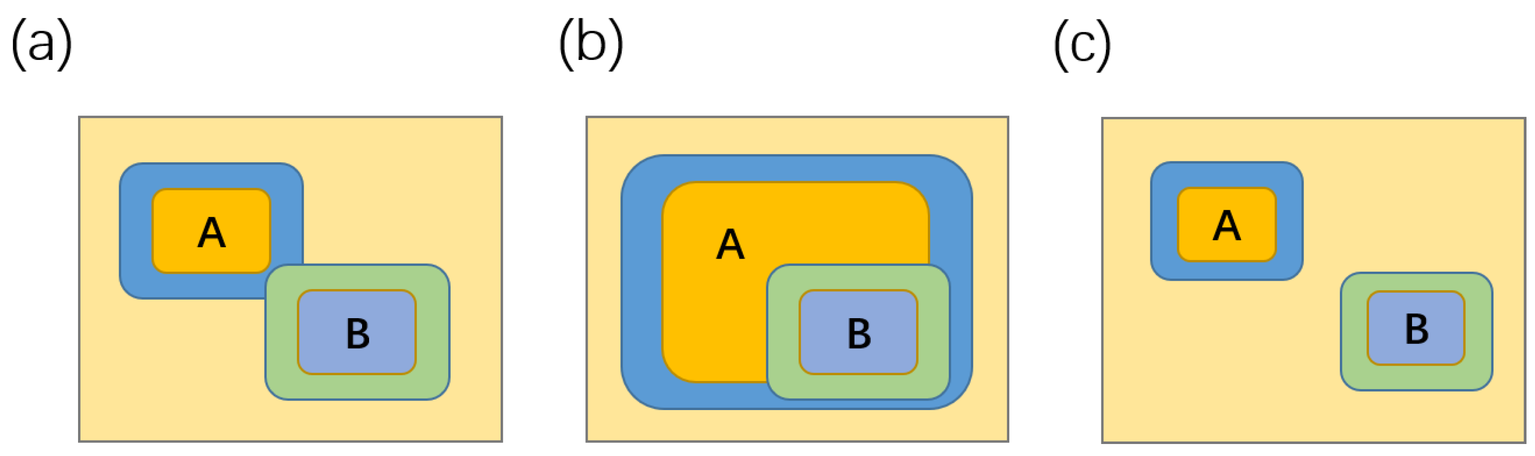
In this paper, the PCell structure of an RFIC device is represented as a rectangle.
Figure 17a illustrates the relative positions of two PCell structures. When two devices intersect, a portion of the contour points of device A enter the contour range of device B. This is known as intersection relationship. On the other hand, when one device fully contains the other device, it is referred to as inclusion relationship. This is illustrated in
Figure 17b, where all the contour points of device B are within the contour range of device A. When there is no intersection between the horizontal and vertical coordinate ranges of the two devices, it is considered a separation relationship, as shown in
Figure 17c. During the layout process, the presence of an intersection or inclusion is considered an error. In summary, when the horizontal and vertical coordinate ranges of two devices intersect, it is regarded as a layout error.
The size vectors of two devices A and B are denoted by
X and
, respectively, and coordinate vectors
P and
of a device can be obtained using Formula (
3). For non-four-port devices, the coordinate vector can be considered a vector consisting of the four vertex coordinates of the device. Therefore, coordinate vector
P can be represented as
, where the abscissa range of the device is
and the ordinate range is
. Thus, the intersection or containment relationship between two devices A and B can be determined as follows [
31]:
To sum up, the evaluation function
is established to judge the positional relationship between devices A and B:
where when the input dimension vector satisfies Formula (
25),
; otherwise,
.
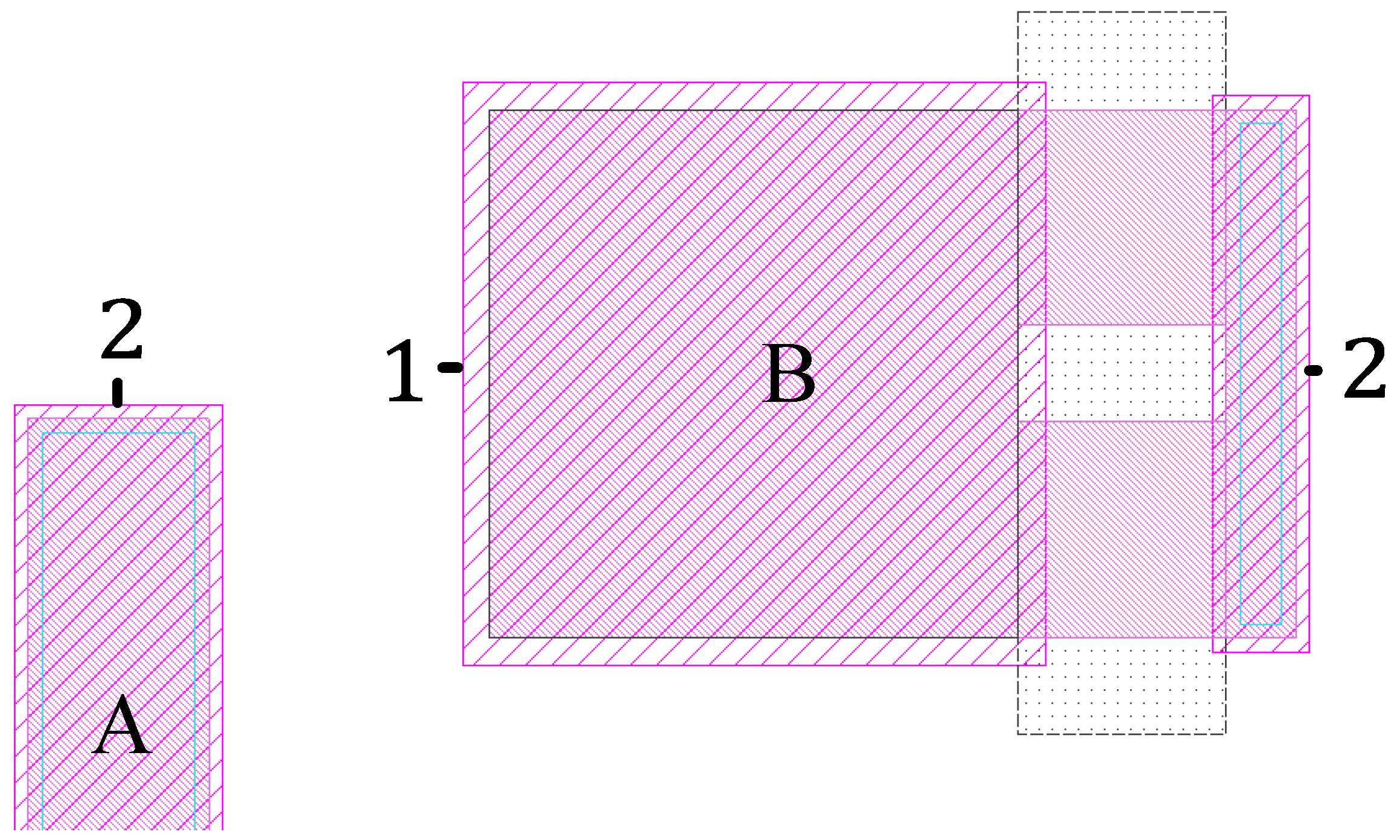
5.3. Rotation and Mirror Operations
This paper represents the physical position of a device using its port 1 coordinates. When rotating the device to achieve the connection of the target port, the port 1 coordinates are necessary. In
Figure 18, the following information is required for splicing port 2 of device B and port 2 of device A: the number of rotations of device B, whether a mirror operation is needed, and the placement coordinates of port 1.
This chapter of the paper introduces a standard port-matching scheme for the Manhattan structure that assigns direction numbers to the four directions of the structure. Specifically, direction 1 is assigned to the left; direction 2, to the right; direction 3, to the bottom; and direction 4, to the top. For instance, in
Figure 18, port 2 of device A is assigned direction 4, while port 2 of device B is assigned direction 2. The chapter also discusses port-matching schemes in the context of rotation and mirror operations, with device A being fixed and device B being spliced with it as a reference.
To reduce the probability of overlapping when layouts intersect, an asymmetric structure can be mirrored. The mirror mode that device B can choose is determined to achieve the normal splicing of the ports. When the connected port of device B points to direction 1 or 2, the optional mirror mode is up-and-down reverse mirroring, as shown in
Figure 19a. On the other hand, if the connected port of device B points to direction 3 or 4, the selectable mirror mode is left-and-right mirror inversion. This is illustrated in
Figure 19b.
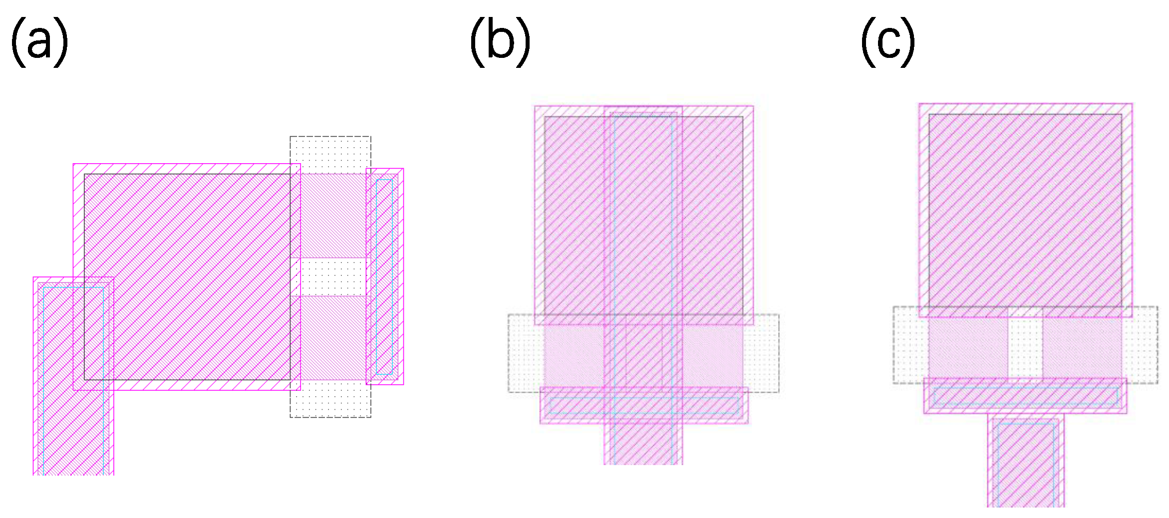
To achieve normal port splicing, it is necessary to determine the physical coordinates and the number of rotations of the other device. In other words, given the physical coordinates of device A, the number of rotations required for device B can be obtained from a lookup table without considering layout overlap.
Table 1 shows the number of rotations required for the port matching of a device based on the direction of the port to be matched.
To summarize, the splicing process for the situation shown in
Figure 18 can be described as follows:
Place port 1 of device B at the port to be matched, as illustrated in
Figure 20a.
Perform three rotations on device B, as shown in
Figure 20b.
Move device B to achieve docking between the two ports using coordinate correction, as depicted in
Figure 20c.
For port
i of the
nth device, the coordinates to be spliced are
. We place port 1 of the
nth device at
, which is represented by the coordinates in its size vector
. The number of rotations is represented by parameter
, while parameter
indicates whether to perform mirroring. Then, for device
n, coordinate vector
after rotation and mirror operations can be calculated using the following formula:
where
A is the addressing matrix and can be obtained with Equation (
3);
M is the mirror operation matrix, which can be calculated using Equations (
11) and (
12); and
R is the rotation operation matrix and can be calculated using Equation (
8).
After rotation and mirror operations, coordinates
of port
i of device
n are
At this point, the two ports to be spliced face each other, but their physical positions may not be aligned. Therefore, physical coordinate correction is necessary. After size correction, coordinates
of port 1 of device
n are
6. The Complete PCell-Splicing Process
To clarify the process, after reading the netlist file, circuit design software generates a list of components and their respective pins. This list contains abstract information about the device, such as its name, size, and pin names, as well as the connection relationship between devices. Based on this connection relationship, the software can determine the order in which the device ports should be connected.
With this information, a splicing process can be performed by reading the port information in the specified sequence. The software can use the formulas and procedures described in this paper to determine the physical coordinates, rotations, and mirror operations needed to connect each pair of ports. By following this process, the software can create a layout that accurately reflects the desired circuit topology.
To process the information in the netlist file, we follow the principle that the number of ports with the same name cannot exceed two [
32]. When the port names are the same, it means that two pins are connected. Based on these principles, we generated an undirected graph containing device information by reading in the netlist file. The pseudocode for reading in the netlist file is shown in Algorithm 1.
| Algorithm 1 Netlist file reading scheme |
| Input: Netlist file. |
| Output: A graph structure containing netlist information: G = (V, E). |
| 1: | port_device = [] |
| 2: | for date in Netlist file do |
| 3: | V.append(date.DeviceInformation) |
| 4: | for in date. do |
| 5: | if port_device[].size() == 1 then |
| 6: | E.append({port_device[][0], date.DeviceName}) |
| 7: | end if |
| 8: | port_device[].append(date.DeviceName) |
| 9: | end for |
| 10: | end for |
| 11: | return G |
In Algorithm 2, the function is used to splice the device layout based on the device name. During the splicing process, when a traceable device is encountered, its device serial number is stored in the stack structure . When an intersection occurs between the layouts, the program backtracks using the serial number in . After the netlist file has been read, the device coordinates, number of rotations, and mirror relationship for the layout with the lowest number of intersections can be obtained. The complete pseudocode for the function is shown in Algorithm 3 below.
| Algorithm 2 Methods for Traversing Undirected Graphs |
| Input: Undirected Graph containing Netlist Information: G = (V, E) |
| Output: Coordinate information of each device: RES |
| 1: | # Convert input graph G(V,E) into an undirected graph represented in adjacency list format. |
| 2: | graph = {} |
| 3: | for v in V do |
| 4: | graph[v] = [] |
| 5: | end for |
| 6: | for e in E do |
| 7: | graph[e[0]].append(e[1]) |
| 8: | graph[e[1]].append(e[0]) |
| 9: | end for |
| 10: | # Depth-first search function for traversing a graph. |
| 11: | STACK = [] |
| 12: | RES = [] |
| 13: | visited = set() |
| 14: | start = V[0] |
| 15: | STACK.append(start) |
| 16: | visited.add(start) |
| 17: | while STACK do |
| 18: | node = STACK.pop() |
| 19: | for neighbor in graph[node] do |
| 20: | if neighbor not in visited then |
| 21: | RES.append(deal_port(node,neighbor) |
| 22: | STACK.append(neighbor) |
| 23: | visited.add(neighbor) |
| 24: | end if |
| 25: | end for |
| 26: | end while |
| 27: | return RES; |
| Algorithm 3 deal_port() function pseudocode |
| Input: DeviceOne, DeviceTwo |
| Output: Device placement coordinate information |
| 1: | if DeviceOne is not placed then |
| 2: | Place DeviceOne randomly |
| 3: | end if |
| 4: | Place DeviceTwo according to the coordinates of DeviceOne |
| 5: | if DeviceTwo intersects with other device then |
| 6: | # Deleting previous layout based on index of reversible components. |
| 7: | num_trace = trace_list.pop() |
| 8: | while history_port_name.top() != num_trace do |
| 9: | Delate(history_port_name.top()) |
| 10: | S.push(history_port_name.pop) |
| 11: | end while |
| 12: | Merro(num_trace) |
| 13: | Rearranging the layout based on the device order in S. |
| 14: | end if |
7. Commercial EDA Software Integration
This implementation method makes it possible to seamlessly integrate the C++ program and ADS, enabling the layout process to be efficiently and accurately automated. The use of AEL scripting provides a high degree of flexibility and customization in the layout process, allowing layouts tailored to specific design requirements to be created.
In addition, the use of ADS as simulation software ensures that the final layout is optimized for radio frequency applications. This is because ADS provides access to a wide range of simulation and analysis tools. This improves the accuracy and reliability of the layout and enables designers to quickly iterate and optimize their designs.
Overall, the combination of C++, AEL scripting, and ADS provides a powerful and efficient solution for automating the layout process in complex circuit designs. This solution can significantly reduce design time and improve design quality.
The structure of the AEL function library’s source code is shown in Algorithm 4.
| Algorithm 4 Part of the AEL library |
| // |
| decl PDK_NAME = “WIN_PL15_1X_DESIGN_KIT”; |
| decl Instance_NAME = list(“ROUND”,“TFR_”,“CAPA_”,“CPW”,“PAD”,“TL”,"Tee”,“Cros”, “Bend”); |
| decl MENTAL = list(“MET1”,“MET2”,“VIA2”); |
| // |
| // |
| defun set_device(kind,x,y,_layout) |
| { |
| decl itemInfo0SP,str; |
| str = strcat(PDK_NAME,“:”,DEVICE_NAME[kind],“:”); |
| // |
| return itemInfo0SP; |
| } |
| // |
| defun roat_device(kind,name_num, roat_k) |
| { |
| // |
| de_rotate_center(-90 * roat_k, TRUE); |
| de_deselect_all(); |
| } |
| // |
| defun move_device(kind,name_num, dx,dy) |
| { |
| // |
| } |
| // |
| defun SET_device(date,kind,x0,y0) |
| { |
| // |
| } |
| // |
| defun merro_device(kind,name_num, sign,x,y) |
| { |
| // |
| } |
8. Results and Discussion
In this study, we developed an algorithm using the C++ programming language to obtain the mapping system and used it to generate the circuit layout. The applicable field of this software is the single-layer circuit layout of RF chips. The workstation used for our experiments used a 2.90 GHz x64 Intel Core(TM) processor with 16 GB of RAM and was tested with a single thread. In the simulation experiment of this paper, the algorithm was tested in two different scenarios.
Rapid production of layout mapping based on netlist files obtained from front-end design: In this scenario, the algorithm was applied to automatically generate a layout for a given netlist file, without manual intervention. The performance of the algorithm was evaluated by comparing the generated layout with the reference layout, and the results show that the algorithm was able to generate accurate layouts with high efficiency.
Rapid circuit reproduction based on physical information extracted with image processing in reverse engineering: In this scenario, the algorithm was applied to extract the physical information of an RFIC device from its microscopic digital photo and use it to generate a layout. The performance of the algorithm was evaluated by comparing the generated layout with the reference layout, and the results show that the algorithm was able to generate accurate layouts with high efficiency.
Circuit layout design is a complex and highly specialized task. With regards to the evaluation of DRC rules in each technology node, the proposed algorithm embraces a rule-based approach that refers to the corresponding PDK library for the specific node. It follows the PDK guidelines and embeds the rules into the algorithm to guarantee that the created layout meets the DRC requirements. However, in some circumstances, design rules may not be available or may lack completeness, resulting in security or other issues. The solution, in such cases, is to depend on the circuit engineer’s experience and judgment to manually verify the layout against the DRC rules. The proposed algorithm is aimed at facilitating engineers in accomplishing preliminary work and reducing the repetitive tasks’ workload, but in the end, the engineer must ensure that the layout aligns with the DRC requirements with manual verification and intervention.
Overall, the algorithm designed in this paper can help RF circuit engineers to accelerate the circuit design process and improve the accuracy and efficiency of layout generation.
8.1. Generating Circuit Layout Based on Netlist Files
Various semiconductor process companies offer their own PDK packages, which can differ significantly from one another. To assess the algorithm’s ability to function effectively across different PDKs, this study examined automatic layout generation by the algorithm under diverse circuit topological logics for PDKs associated with two different processes. The topological logic of the test circuit is provided as a netlist file, whose content format is detailed in
Table 2.
The resulting layout schemes are presented in
Table 3. By utilizing a self-written AEL function library to call ADS across platforms, the layout was completed in ADS. The algorithm was found to avoid the intersection of layouts and produced circuit layouts that conformed to the production specifications for radio frequency circuits. The splicing effect of this algorithm was found to be superior to that of the default layout mosaic splicing effect provided by ADS, as verified with algorithm verification.
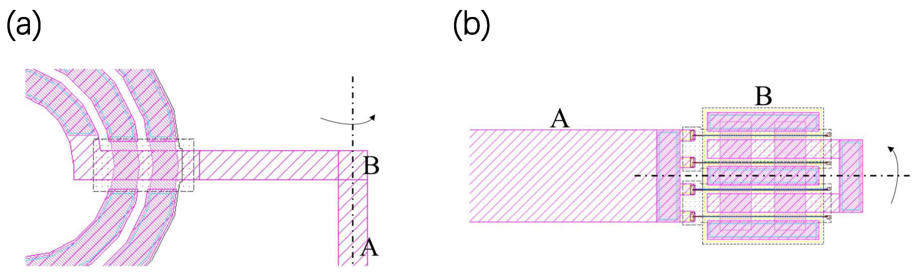
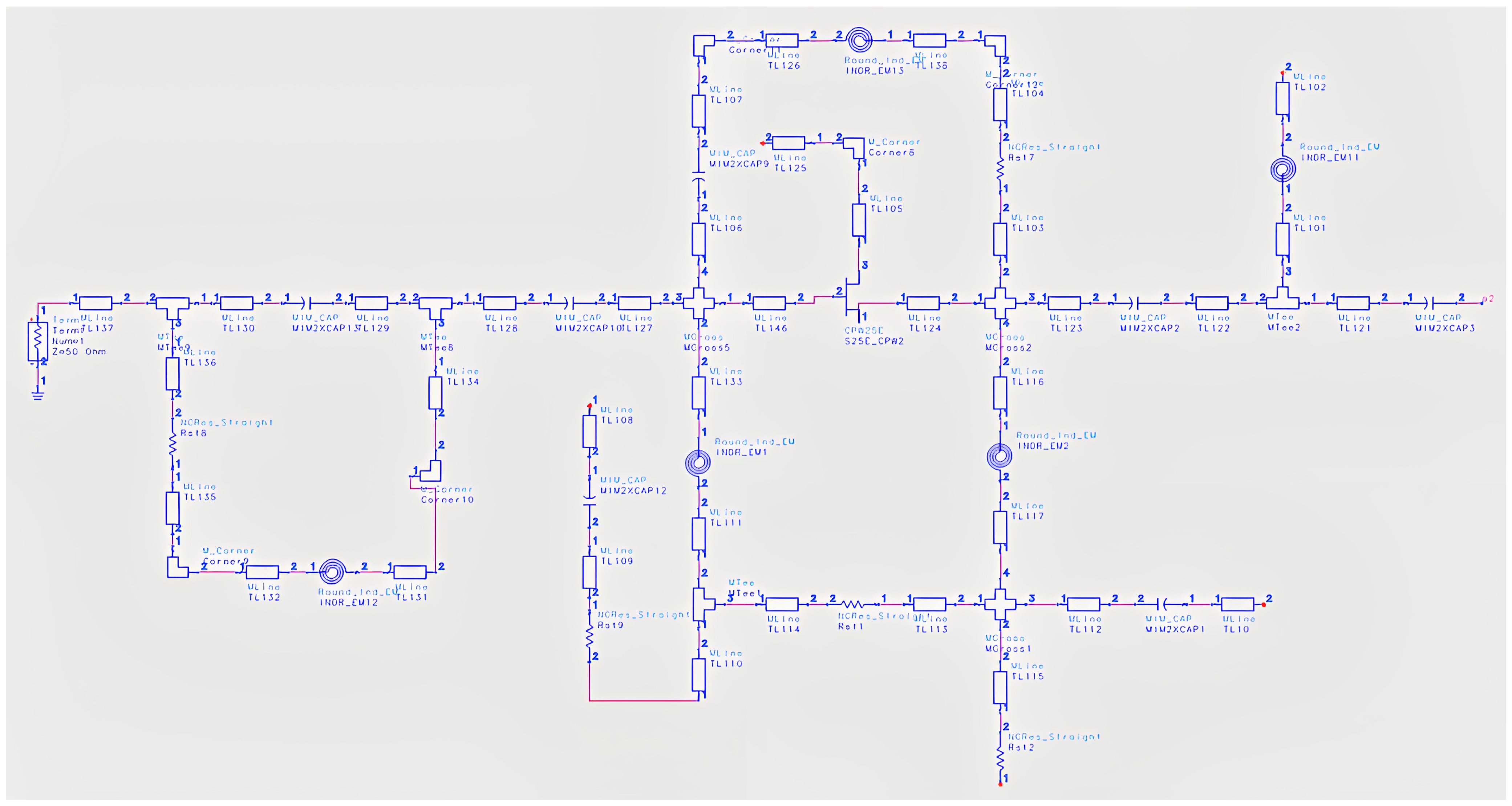
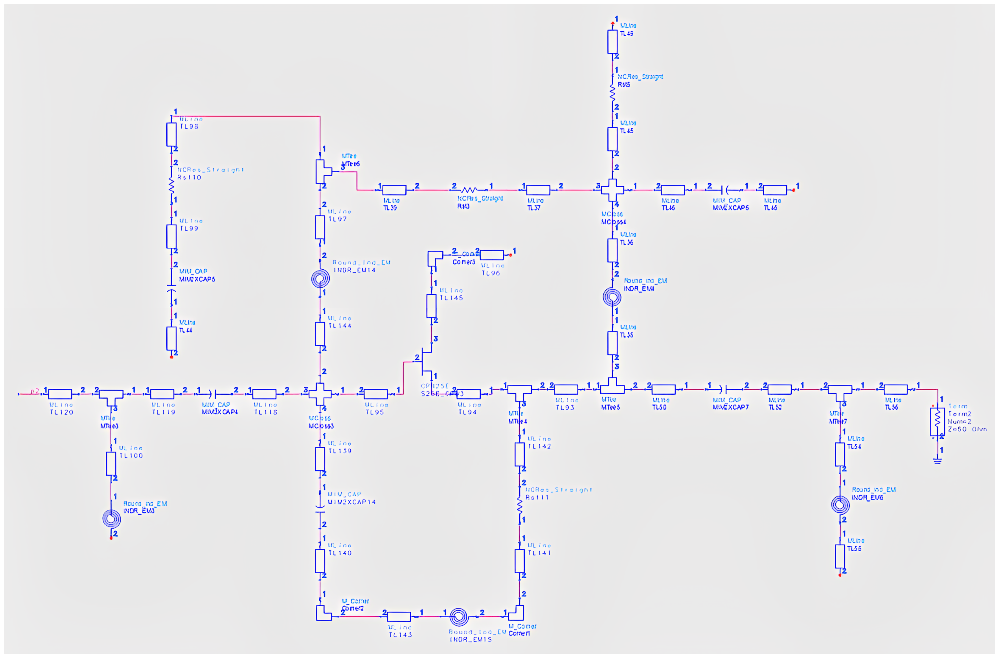
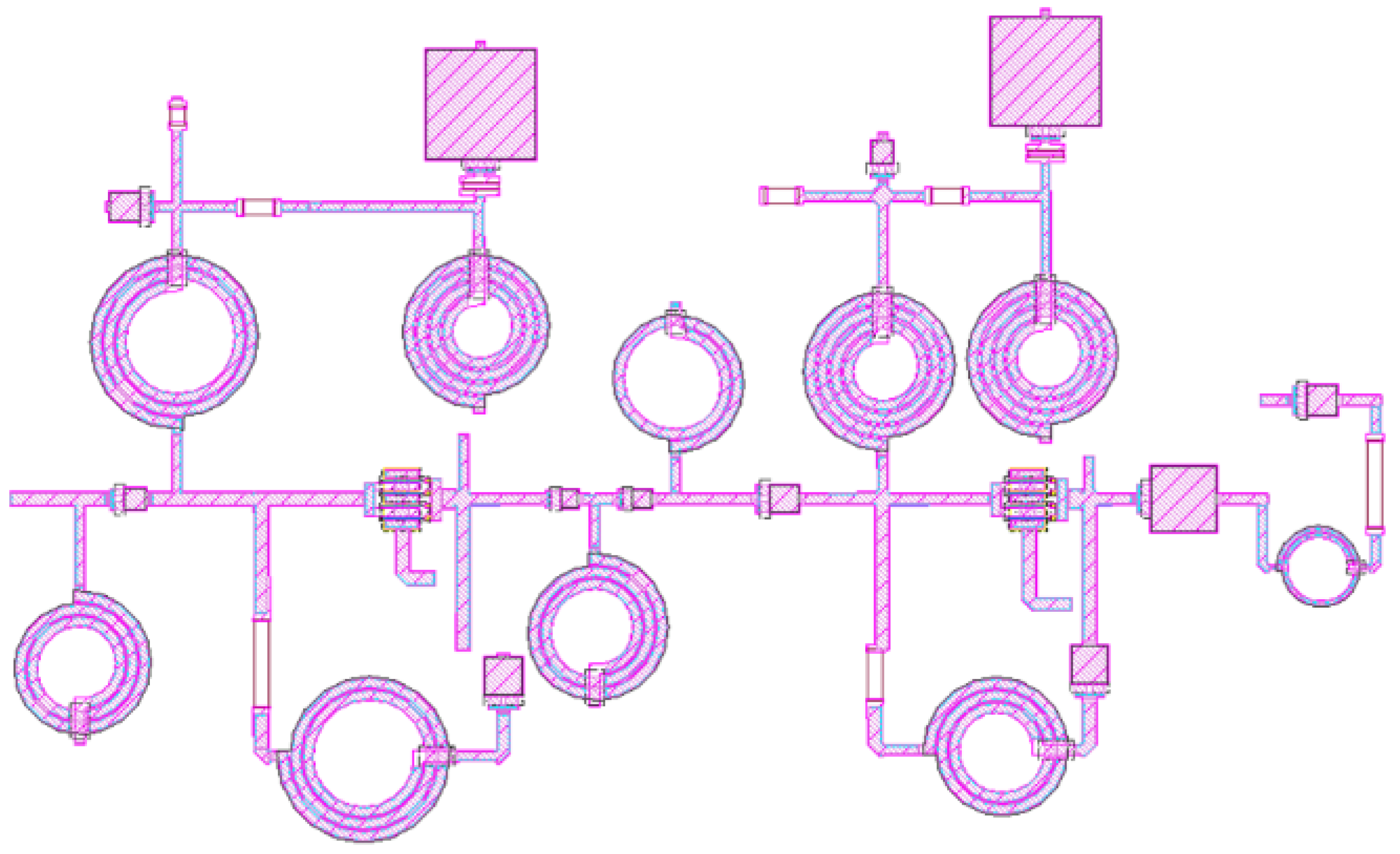
The algorithm was tested on an RF low-noise amplifier with five ring structures using the PDK process by WIN Company. For the convenience of circuit schematic display, we divided the schematic into two parts and connected them with a pin named p2. The schematic displays are shown separately in
Figure 21 and
Figure 22.
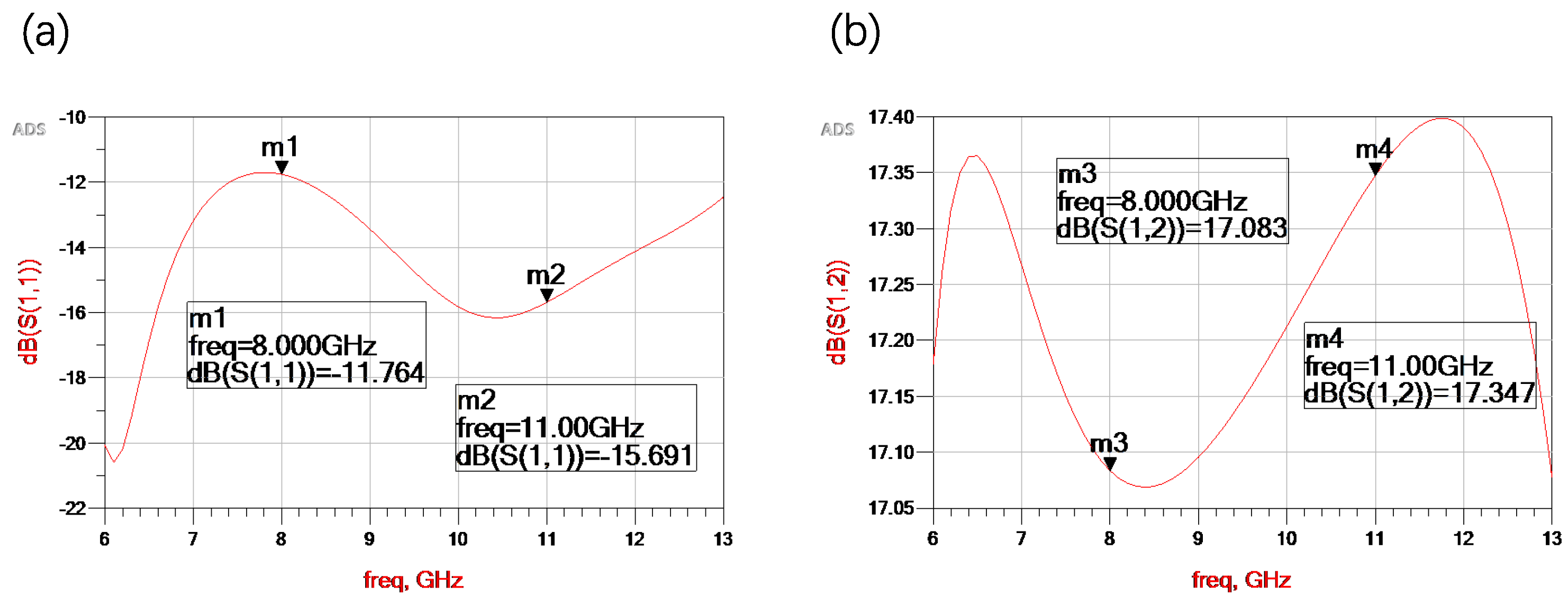
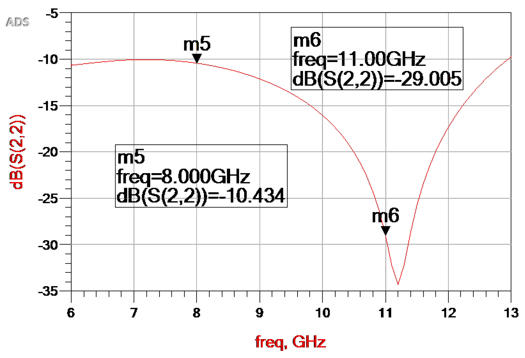
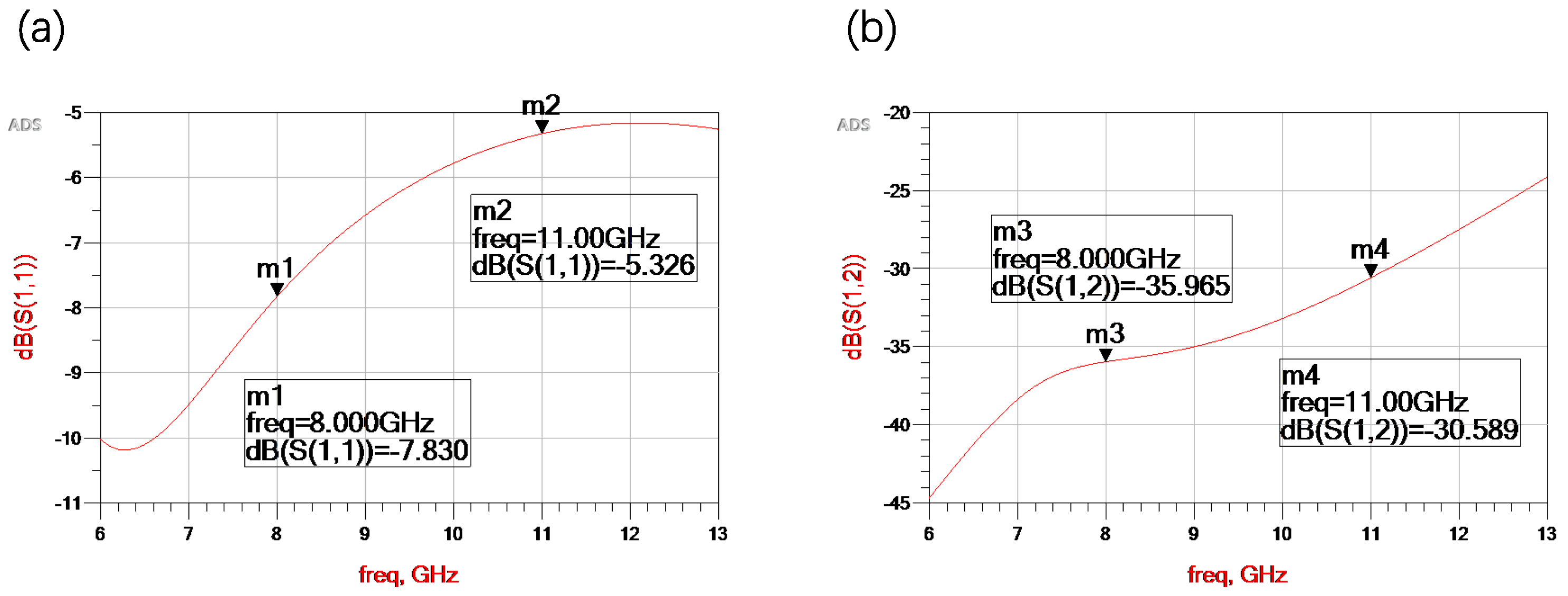
The simulation results of the circuit schematic are illustrated in
Figure 23 and
Figure 24. This circuit is a low-noise amplifier operating in the frequency range of 6–13 GHz. As can be observed from the figures, both S11 and S22 of the simulation results are less than 10 dB within the operating frequency band. The simulation result of S12 is around 17 dB, demonstrating the high potential of this design chip.
The resulting layout, obtained from the input circuit netlist file, is shown in
Figure 25. As seen from the figure, the algorithm-generated layout avoided the intersection of devices. Although the closure of the five ring structures could not be achieved due to device parameters, the connected parts in the layout were positioned at the shortest physical distance, making the circuit layout conform to the production specifications of the radio frequency circuit. This layout generation took 86 ms, and the generated layout area was 1919 × 1176
m
2.
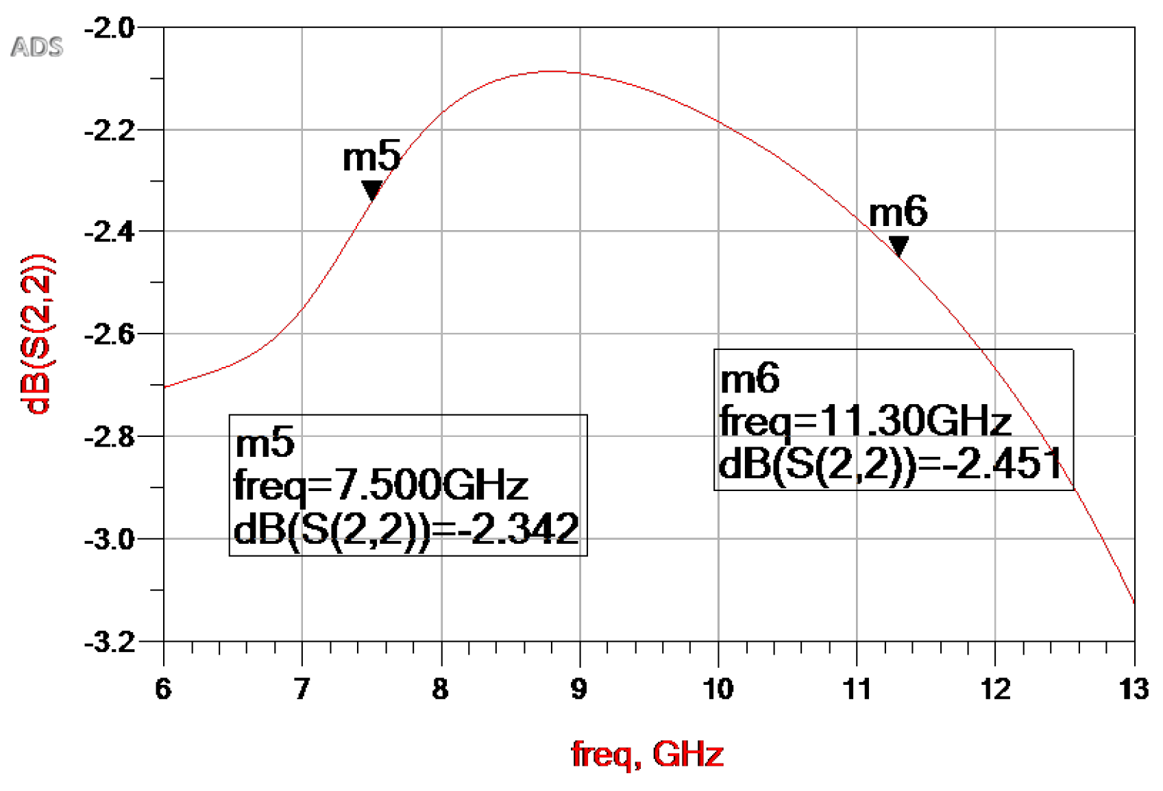
The circuit simulation based on algorithm-generated layouts is shown in
Figure 26 and
Figure 27. As can be seen from the simulation results, there are discrepancies between the back-end simulation results and the front-end results, which require engineers to further debug the layout to optimize its performance. The algorithm proposed in this paper serves as a tool to aid engineers in completing the preliminary work of back-end design, reducing the workload of repetitive tasks. However, ultimately, engineers need to perform performance debugging to ensure that the layout performance meets production specifications.
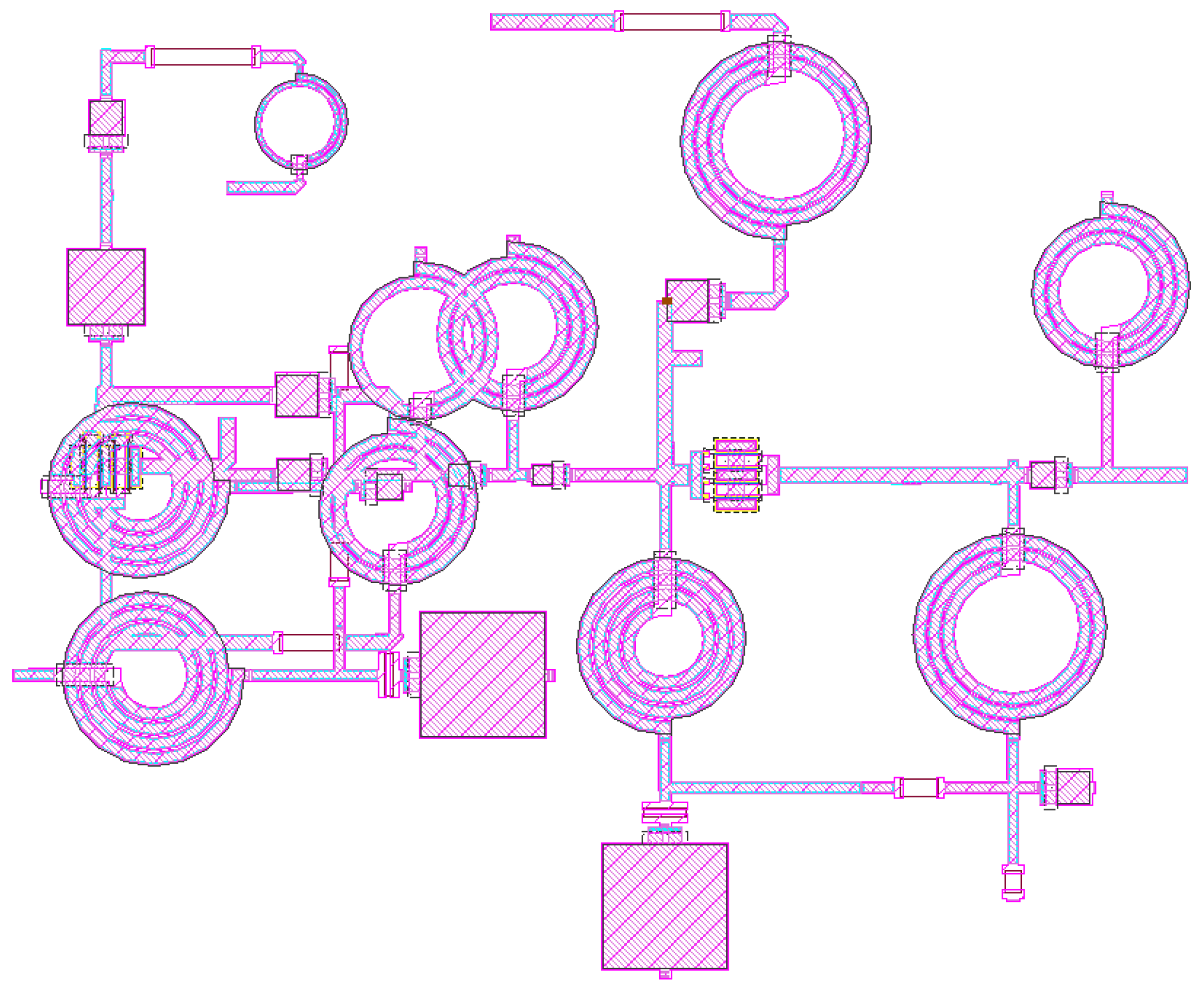
ADS software provides built-in tools for generating circuit layouts. To compare the results of these tools with the algorithm proposed in this paper, the same circuit topology was used to generate layouts using the built-in tools in ADS, as shown in
Figure 28. The layout generated by ADS appears chaotic, with many intersections. Based on the verification conducted in this study, the algorithm proposed in this paper demonstrates a superior splicing effect when compared with the layout mosaic tool provided in ADS.
8.2. Layout in Reverse Engineering
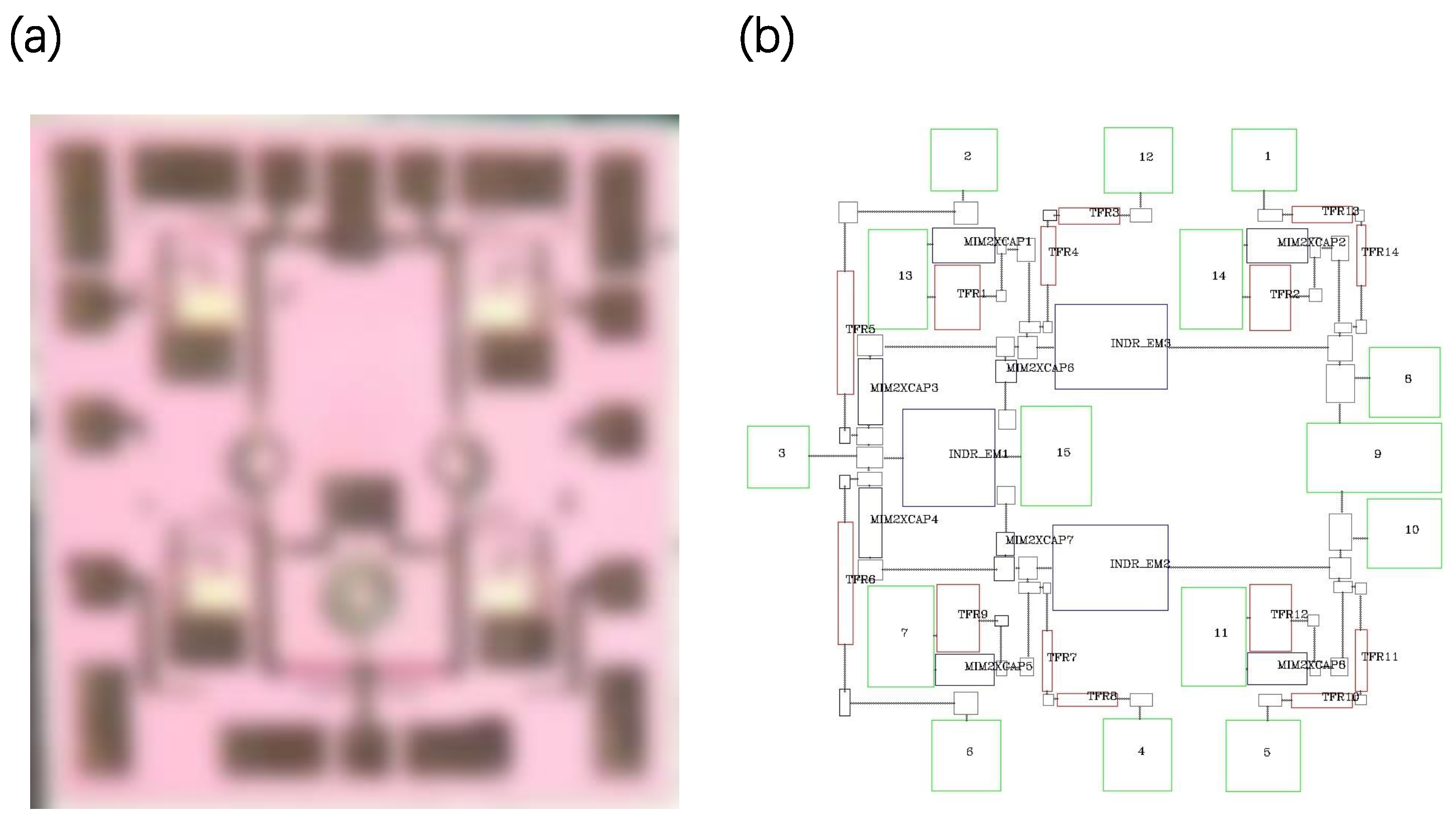
The algorithm presented in this article has potential applications in the reverse engineering of circuits. Specifically, it can assist engineers in reproducing circuits based on extracting physical information from chip photos taken under a microscope, which can save a lot of human resources during process migration. To illustrate the efficacy of the algorithm, an SPDT switch chip was used as an example. This switch operates in the frequency range of 8–12 GHz and is highly suitable for many applications, such as radar systems, medical equipment, and wireless communication devices. Physical information was obtained with microscopic analysis, and a layout algorithm was then utilized to generate the board layout. The resulting layout was subsequently subjected to simulation testing.
Figure 29a displays a blurred photomicrograph of the chip under a microscope to safeguard the circuit IP. The information extraction algorithm was then utilized to extract physical information such as device parameters, circuit topology, and device port coordinates from the digital photo. The resulting circuit topology is shown in
Figure 29b. The chapter focuses on the PDK technology provided by Lion and demonstrates how the algorithm can be utilized for achieving process migration and layout reproduction for the circuit.
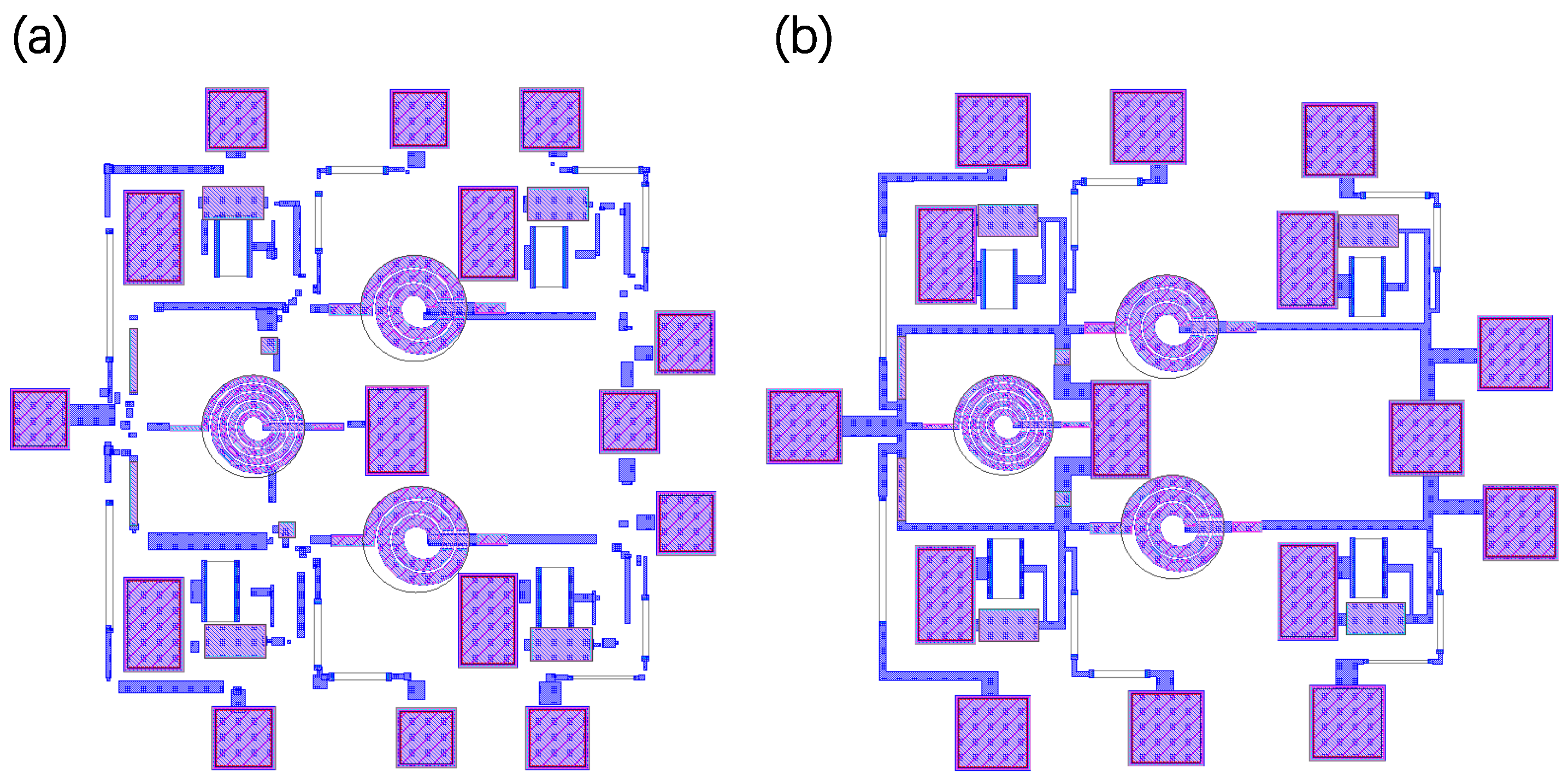
The algorithm started by setting the device PCell parameters based on the extracted device parameters and placing the PCell devices according to their relative positions in the photo to obtain an initial layout, as shown in
Figure 30a. However, the initial layout had overlaps between PCell devices and broken port splicing. To address these issues, the proposed algorithm was used to polish the layout, resulting in a final layout as shown in
Figure 30b. This layout generation took 124 ms, and the generated layout area was 913 × 898
m
2.
The generated layout underwent simulation testing. As shown in
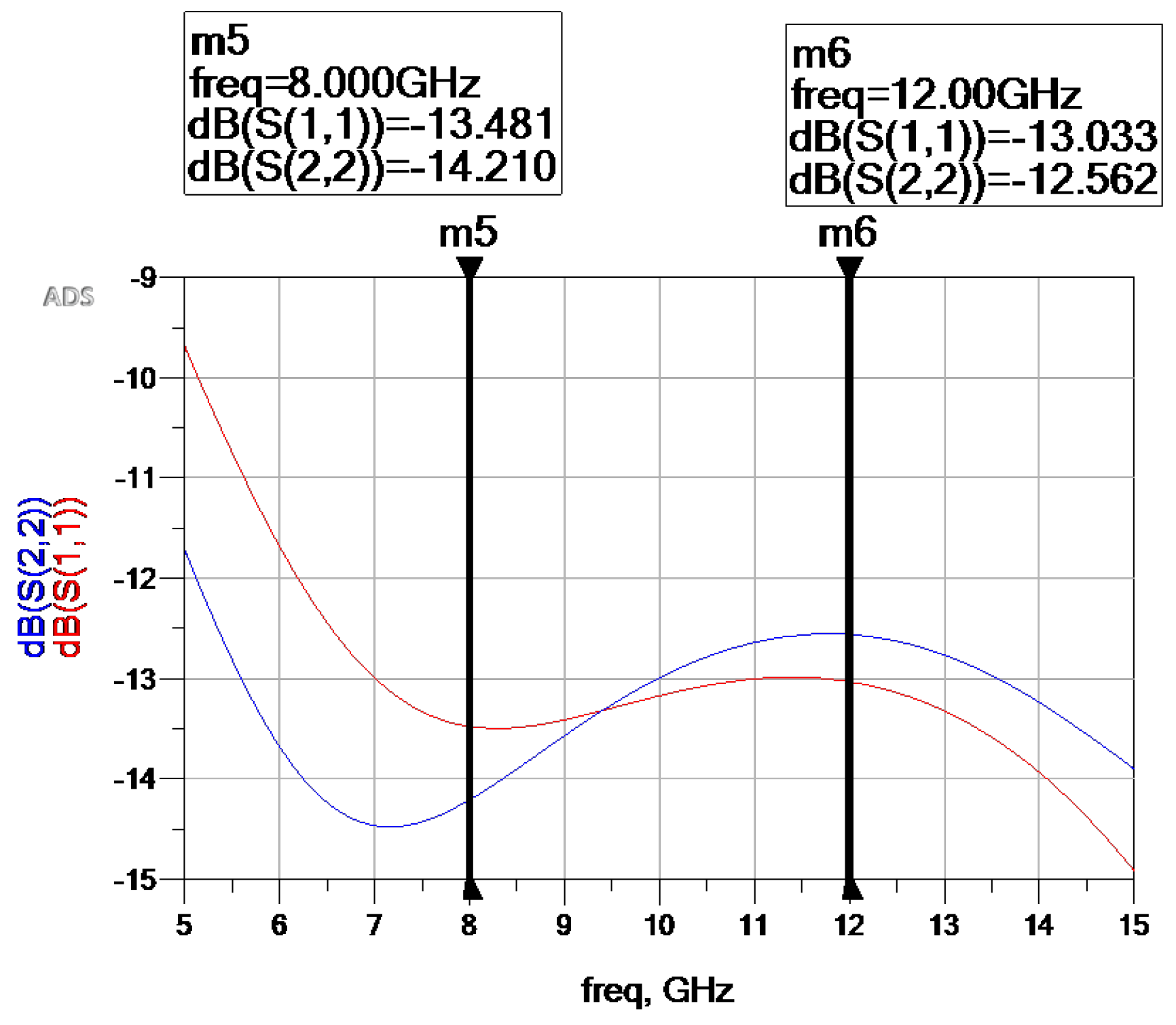
Figure 31, the circuit exhibited return loss (S11 and S22) that was superior to −20 dB within the 8–12 GHz frequency range, indicating minimal reflected energy and optimal impedance matching within the design. Moreover,
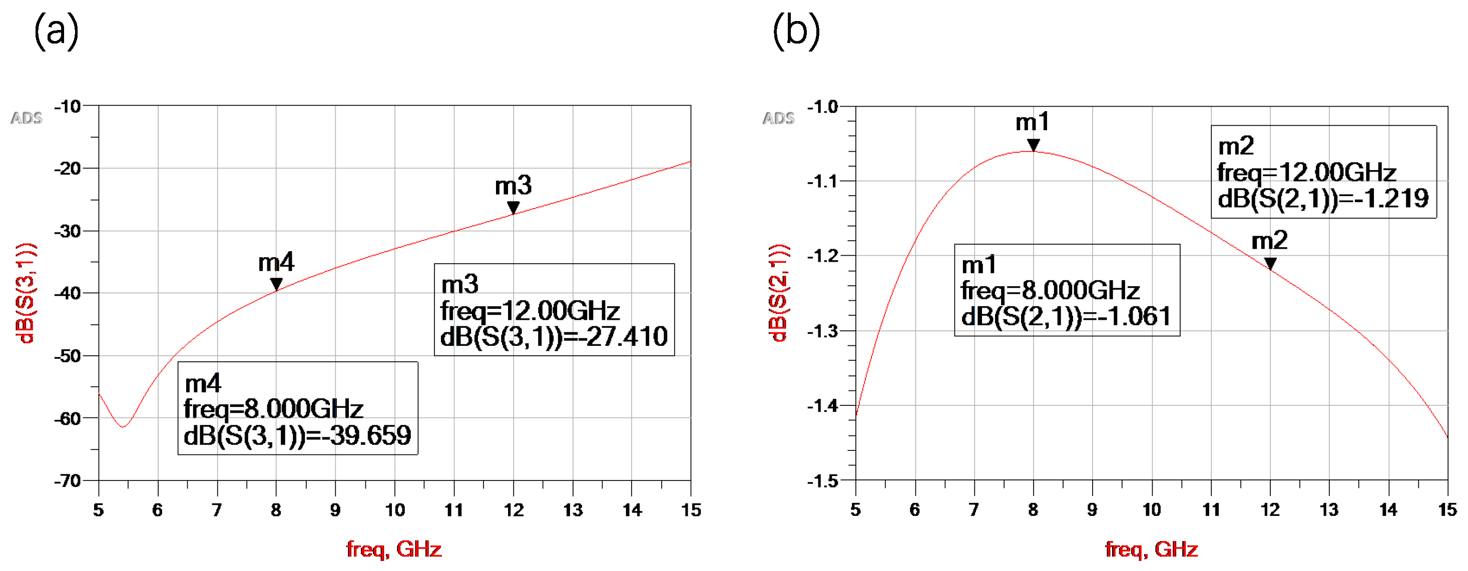
Figure 32a depicts the switch’s isolation (S31) to be less than −20 dB within the bandwidth, reflecting an excellent separation of signals between the input and the two output ports. Additionally,
Figure 32b indicates that the insertion loss (S21) was greater than −1.5 dB, denoting efficient transmission of input signals to output ports. In light of these observations, the switch layout is regarded as performing well and possessing considerable potential for eventual adoption in practical applications.
Overall, the algorithm presented in this article provides a useful tool for reverse engineering circuits and can save significant human resources during process migration. The scope of the frequency range that can be designed depends on the specific circuit requirements and the capabilities of the layout design tool. However, for the case presented in this article, the engineer was able to design circuits with a frequency range of DC to 15 GHz. This covers a wide range of frequencies commonly used in RF applications, including those used in 5G and 6G communication systems. It is worth noting that designing circuits for higher frequencies, such as those in the millimeter-wave range, can be more challenging due to the increased sensitivity to parasitic effects and the need for precise layout optimization.
9. Conclusions
This paper presents a novel algorithm for the layout design of radio frequency circuits. The algorithm is based on the depth-first search framework, which considers the connection relationship between the PCell structure/basic device structure and circuit topology to automatically generate an orderly layout. The proposed algorithm offers better results than ADS-related modules in the experimental phase. The algorithm addresses the issue of the lack of layout stitching tools for RF circuits in the automatic design problem. It also assists engineers in traditional RF circuit design in completing the mapping from schematic diagram to layout, thereby reducing manpower costs. Overall, the proposed algorithm offers a promising solution for the automated layout design of RF circuits.
Regarding the evaluation of DRC rules in each technology node, the proposed algorithm adopts a rule-based approach that refers to the corresponding PDK library for the specific technology node. The algorithm is designed to follow the PDK guidelines, and the rules are incorporated into the algorithm to ensure that the generated layout meets the DRC requirements. However, in some cases, due to security reasons or other factors, the design rules may not be available or may be incomplete. In such situations, the solution is to rely on the circuit engineer’s experience and judgment to manually verify the layout against the DRC rules. The proposed algorithm serves as a tool to aid engineers in completing the preliminary work and reducing the workload of repetitive tasks, but ultimately, the engineer needs to ensure that the layout meets the DRC requirements with manual intervention and verification.
At present, the netlist file needs to be provided by the circuit engineer, either from the front-end design results of the circuit or from the physical information of the chip collected under the microscope during reverse engineering. However, in future research, it may be possible to integrate a comprehensive method for netlist design into the algorithm, which would further streamline the circuit design process.


