Article

Utilizing Full Degrees of Freedom of Control in Voltage Source Inverters to Support Micro-Grid with Symmetric and Asymmetric Voltage Requirements

by
Akhtar Rasool
1,*,
Fiaz Ahmad
2,
Muhammad Salman Fakhar
3,
Syed Abdul Rahman Kashif
3 and
Edwin Matlotse
1
1
Department of Electrical Engineering, University of Botswana, Gaborone UB 0061, Botswana
2
Department of Electrical and Computer Engineering, Air University, Islamabad 44000, Pakistan
3
Department of Electrical Engineering, University of Engineering and Technology, Lahore 54000, Pakistan
*
Author to whom correspondence should be addressed.
Symmetry 2023, 15(4), 865; https://doi.org/10.3390/sym15040865
Submission received: 31 January 2023 / Revised: 13 March 2023 / Accepted: 22 March 2023 / Published: 5 April 2023

Abstract

:
This article proposes a novel equivalent control method for voltage source inverters (VSI) with disturbance observers (DOB) to support the symmetric and asymmetric voltage requirements of a micro-grid (MG) while also matching the MG output power requirements. The method leverages the degrees of freedom (DOF) of the VSI under symmetric and asymmetric MG voltage conditions by utilizing the mean-point voltage of the MG, which is often overlooked in literature studies due to this being grounded. The method enables the three-phase inverter to generate voltages as needed by the MG inconsistently due to changing loads in the MG circuits or phases. The method is also insensitive to disturbances because of the DOB, being part of the controller. The proposed method is validated under both the balance and imbalance voltage demands of the MG. The mean voltage of the MG is used as a set-point to be corroborated as a mean voltage at the inverter’s output, in addition to active-reactive power references. The novel model is developed by augmenting the new, mean-point voltage as part of the system dynamics. The proposed method is simulated in MATLAB/Simulink® and is verified for its hardiness and effectiveness.

1. Introduction

With the advent of modern applications and the expanding populations of cities, the demand for electricity is increasing unchecked. This demand is bringing a great deal of pressure on the already functioning power system’s infrastructure. Not restricted to the infrastructural issues only, power generation is also being constrained by the limited fossil fuels and changing trends towards clean and renewable energy options. The renewable energy sources (RES) have their own challenges because of their fluctuating nature, thus leading to open problems to be solved by the research and development community [1,2].
The smart grid (SG) is a modern paradigm of power systems, compared to its traditional version, due to having the state of the art of all engineering and scientific fields merged into one system. SG is a novel framework due to its bidirectional power flows, smart data acquisition methods, remote data operations, smart diagnostics, desirable monitoring, smart communications, distributed controllers, smart energy sharing, consumer participation, renewable energy integration, re-configurable capability and smart conversion functions [1,2,3]. SG is realized by the integration of MG units, while also connecting it to the upstream power network. MG is a local power system architecture and autonomously controllable power unit, which can function in isolation or in grid-connected modes. MG is generally formed by the integration of RES or by the integration of distributed generators (DGs), where every DG is either based on fuel cells, wind or solar energy. Every DG also functions in a self-controllable manner so as to optimize the energy generation and to meet the needs of the MG [4]. The structure of the MG composed of DGs, depending upon VSI, is given below in Figure 1 [5].
DG’s main causes of tripping from the MG are voltage variations (swell or sag), which are either due to fault conditions or impedance mismatches among the phase circuits of the MG. This tripping of DGs can cause a serious imbalance in the MG circuit, leading to total blackouts. For this reason, grid codes (GCs) suggest three demands [6]:
  • The DG must stay connected to the MG for up to 150 ms, even if the MG voltage drops to zero.
  • The DG must support voltage recovery by injecting a reactive current into the MG.
  • The DG must ramp up the active power to normal operation immediately after clearing the imbalance or fault.
Therefore, DGs are required by the GCs to maintain the MG voltage or MG frequency within the required range and is a matter of converter control. The role of power converters is very unique since the converters are the interfaces enabling the synchronization, voltage control, current control and power flow control in the MG and SG [5,7,8]. A number of studies can be found in the literature regarding the control of three-phase VSI, specifically in view of controlling the imbalance of power in the MG [9,10,11,12,13]. All of these established works offer complexity, since they are designed to maintain pure sinusoidal voltages as the output of the VSI, whose conception dates back to the 1980s due to the stringent supply requirements of the three-phase motors [14,15,16,17].
In order to supplement the compensations for the imbalances produced on the grid side, a number of research and control formulations have been applied to VSI. The sliding mode control (SMC) method has also been applied, considering that the converters have switching devices, which in nature are discontinuous and quite consistent with the adopted control technique [18,19]. However, all of these studies are found employing two-dimensional control, which results in the under-utilization of the capabilities of three-phase converters [20,21,22,23].
The unknown variables or the control constituents in any system are known as the degrees of freedom (DOF), which are two in the case of three-phase converters in the synchronous reference frame, meaning that the third degree is free for utilization [22]. The random nature of the loads in the distribution system connected to the MG introduces a demand for imbalance voltage generation or imbalance current compensation from the VSI. This asymmetric voltage generation demand from the VSI requires it to employ the full capabilities (DOF) of its switching matrix [24]. All three-phase converters have three independent control inputs but, in general, in all techniques, the desired outputs are defined either as control of current (orthogonal dq-/ α β -frames) or control of power (active and reactive, power frames), resulting in 2D control requirements. Hence, the target is to use the third DOF to provide a much needed and desired output in addition to two orthogonal currents or powers.
In this article, the superfluous DOF available in the VSI’s switching matrix is used for the voltages’ asymmetry as an additional requirement to bring a balance between the MG (with loads) and the VSI source. The organization of the paper follows in a logical manner. First, the system’s novel model is developed, and then the novel control formulation is established, and finally the simulation results are described to demonstrate the method’s robust and vigorous performance.

2. System’s Modeling

The renewable energy system’s output can be modeled using a DC link capacitor, which, through a VSI, a 3-phase filter, and a 3-phase inductance (equivalence of transmission line), is connected to a 3-phase MG. The grid is considered to be working either in balance or in imbalance conditions due to the contingent nature of the real-time loads or the occurrence of faults. A generalized diagram of the VSI source connected to the three-phase MG is given in Figure 2.
The active and reactive or orthogonal powers can be evaluated at the MG end using expression (1).
P g Q g = v g T · i g v g T · i g = v g T i g v g T i g
where
v g T = vector orthogonal to MG voltage vector ( v g T ) v g T = [ v g a v g b v g c ] = voltage vector of MG i g T = [ i g a i g b i g c ] = current vector of MG .
Taking the derivatives of power (1) yields
P g ˙ Q g ˙ = v ˙ g T i g + v g T i g ˙ v ˙ g T i g + v g T i g ˙
Considering the L g values to be zero in Figure 2, Kirchhoff’s voltage law gives the grid current expression to be
L g d i g d t = v c v g R g i g
Now, substituting the grid current dynamics into Equation (2), the following dynamics of active/reactive powers are obtained.
P g ˙ Q g ˙ = v ˙ g T i g L g 1 v g T v g + L g 1 R g v g T i g v ˙ g T i g L g 1 v g T v g + L g 1 R g v g T i g + L g 1 v g T v g T v c
If the errors in the orthogonal powers’ exchange are denoted by e P g , e Q g and the set-points for these powers are represented by P g r e f , Q g r e f , then the dynamics of errors for these powers’ ( e ˙ P g , e ˙ Q g ) exchange can be given as below [24]:
e ˙ P g e ˙ Q g = P ˙ g r e f v ˙ g T i g L g 1 v g T v g L g 1 R g v g T i g Q ˙ g r e f v ˙ g T i g L g 1 v g T v g L g 1 R g v g T i g L g 1 v g T v g T v c
where
L g = diagonal MG inductance matrix of order 3 × 3 R g = diagonal MG resistance matrix of order 3 × 3 v c T = [ v c a v c b v c c ] = converter voltage vector .
It is obvious from Equation (5) that the converter output voltage components ( v s T ) are independently affecting the orthogonal power exchange between the RES and the MG, since both the powers are reliant on the collinear vector of the MG voltage ( v g T ) and the orthogonal vector of the MG voltage ( v g T ). As seen in Equation (5), the vector of control ( v c T ) has 3 constituents, while the vector of control error ( e PQ T ) has 2 constituents. Consequently, there is a possibility to use the third available superfluous degree in the vector of control ( v c T ) so as to enforce or satisfy a new requirement of the system, which will accomplish the utilization of the full control capabilities of the VSI. Writing Equation (5) in a compact form yields
e ˙ P g e ˙ Q g = P ˙ g r e f f P Q ˙ g r e f f Q L g 1 v g T v g T v c
where
f P = disturbance terms of active power of order   1 × 1 f Q = disturbance terms of reactive power of order   1 × 1 .
Now, it is important to mention that in the case of a balanced or symmetric MG, the average of the 3-phase voltages equals zero, as denominated by point ( v g n ) in Figure 2. However, in the case of an imbalanced or asymmetric MG, the average of the 3-phase voltages results in an instantaneous, non-zero value due to the stochastic nature of the real-time loads connected to the MG. It is important to highlight again that this MG’s neutral value ( v g n ) is generally considered to be grounded in the literature [20,21,22,23] and negative sequence control schemes are used to compensate for the imbalances appearing in the form of a negative sequence in the MG. Contrarily, in this article, the mean voltage ( v g n ) of the MG is kept floating and also it is used as an additional requirement of the MG, which is reflected towards the generation side (or the RES-based VSI source side) as a desired additional reference value. In order to obtain the desired results, it is specified in the error dynamics form as given below in Equation (7):
η ˙ = f η L g 1 b T v c = v g n v c n
where
f η = disturbance terms of mean MG voltage of order   1 × 1 v g n = 1 3 ( v g a + v g b + v g c ) = mean voltage of MG of order   1 × 1 v c n = 1 3 ( v c a + v c b + v c c ) = mean voltage of VSI of order   1 × 1 b T = [ 1 3 1 3 1 3 ] = mean voltage magnitude vector of order   1 × 3 .
where the novel variable dynamics ( η ˙ ) show the rate of change for this contemporary voltage requirement ( η ) of the MG to be produced by the VSI.
After augmenting the newly introduced dynamics (7) of the new requirement into the power control error dynamics (6), the final and complete control error dynamics are found to be
e ˙ P g e ˙ Q g η ˙ = P ˙ g r e f f P Q ˙ g r e f f Q f η L g 1 v g T v g T b T v c
Further, in a more compact form, the errors of dynamical system (8) can be mentioned in matrix form as below:
e ˙ P Q η = f P Q η + B P Q η v c
In Equations (8) and (9), the dimensions of the error vector ( e ˙ P Q η ) are matched with those of the control vector ( v c ) and, according to the basic control theory, the system (9) is now fully controllable because the distribution matrix of control ( B P Q η ) has full rank. Further, as the system (9) is not rank-deficient, a unique transformation ( x = T e P Q η ) is now possible in such a way that the new system ( x ˙ = f x + B x v c ) has a diagonal control distribution matrix ( B x ). Hence, the new converted system is a dynamically decoupled system and has three first-order, decoupled sub-systems. One sub-system corresponds to the active power, the second to the reactive power and the third sub-system corresponds to the mean-point voltage of the MG, meaning that the system has been transformed into a one-on-one function system.
Now, the non-singularity of the control distribution matrix ( B P Q η ) completely depends upon the selection of the third row vector ( b T ), since the first and second rows already have vectors, which are orthogonal. It means that the variable ( η ) has to be selected carefully so that it meets the requirements as defined above. It is now important to highlight that the zero-sequence voltage or zero-sequence current cannot exist in a balanced, 3-phase system, but these sequences do exist in an unbalanced, 3-phase system. Accordingly, the variable ( η ˙ ) has been formulated in such a way as to make the zero-sequence voltage of the VSI output v c n = 1 3 ( v c a + v c b + v c c ) to track the grid’s zero-sequence voltage v g n = 1 3 ( v g a + v g b + v g c ) , and the three-phase output voltages ( v c T ) of the inverter are generated so as to meet the zero-sequence voltage ( v c n ) of the VSI. Hence, in the system (8), selecting the third variable as η ˙ = v g n v c n will achieve the desired output voltages for the MG.

3. Control Formulation

As found in the above section, the variable η ’s selection is constrained by the need that the distribution matrix of control ( B P Q η ) must not be rank-deficient. As per the literature, the third variable ( η ) can help to generate balance voltages in converters for ac machines by using any non-linear control technique [18]. On the other hand, the zero-sequence voltage or current exists for the imbalance scenario, i.e., the reference for η does exist, which means that the zero-sequence voltage of the MG ( v g n ) can be tracked by the zero-sequence voltage of the inverter ( v c n = 1 3 ( v c 1 + v c 2 + v c 3 ) ). This can be achieved by selecting η ˙ = v g n v C n . Hence, it leads the control formulation to lie within the ( P , Q , η ) -frame of reference (FOR), in contrast to ( P , Q ) / ( d , q ) -FOR present in most of the literature [20,21].
Accordingly, the choice of the control variable from (9) can be made as below:
v c = B P Q η 1 f ^ P Q η + K P Q η e P Q η
where f ^ P Q η depicts the estimation of the f P Q η , yielding closed-loop error dynamics to be
e ˙ P Q η + K P Q η e P Q η = f P Q η f ^ P Q η
It is obvious from (11) that the control errors will diminish to zero and the references will be tracked provided that the estimation of f P Q η is such that f ^ P Q η f P Q η , ∀ K P Q η > 0 .
Considering the pair e P Q η , v c calculable, having ( f P Q η ) as an input, which is undecided but fulfilling ( f ^ P Q η = 0 ), then the dynamics of the new system ( z = f P Q η L e P Q η ), where L > 0 can be mentioned as z ˙ = L z + L e P Q η + B P Q η v c . This system helps to calculate z , thus estimating the unknown input as f ^ P Q η = z + L e P Q η . Then, taking suitable values of L > 0 will separate the dynamics of the observer from the closed-loop dynamics, resulting in f ^ P Q η f P Q η and thus e P Q η 0 . Hence, the selection v c = B P Q η 1 f ^ P Q η + K P Q η e P Q η confirms the power control and maintains the additional, novel requirement η 0 . Notice that v c is continuous.
Further, in order to complete the control design, the kinetics of the inductor currents and capacitor voltages may be evaluated from Figure 2 as given in the equations below:
d d t i L f a i L f b i L f c = L f 1 v c a v c b v c c + L f 1 v A v B v C
d d t v c a v c b v c c = C f 1 i g a i g b i g c + C f 1 i L f a i L f b i L f c
d d t v d c = C d c 1 i R E S i Lf T s ; s T = s 11 s 12 s 13
v A = v d c s 11 v B = v d c s 12 v C = v d c s 13
s 1 k = 1 , if the switch ( s 1 k ) is closed and the switch ( s 2 k ) is open 0 , if the switch ( s 1 k ) is open and the switch ( s 2 k ) is closed
Here,
i R E S = current to/from RES v d c = DC-bus voltage C d c = DC-bus capacitor L f = filter inductance diagonal matrix C f = filter capacitance diagonal matrix i Lf T = [ i L f a i L f b i L f c ] = inductor/converter o/p current vector i g T = [ i g a i g b i g c ] = converter o/p current vector supplied to grid v c T = [ v c a v c b v c c ] = o/p voltage vector at PCC v s T = [ v A v B v C ] = voltage vector at o/p of switching matrix s T = [ s 11 s 12 s 13 ] = converter switching vector
s T is the switching vector, which is used to determine the condition of the switches within the switching matrix. If the voltages ( v A , v B , v C ) are taken as control inputs, then the dynamics (10)–(16) constitute discontinuous inputs of control, and the voltages ( v c a , v c b , v c c ) are controlled outputs. As given in Equation (10), the already evaluated voltage ( v c ) is to be used to maintain the wanted power flow, so it can be employed to determine the set of three-phase voltages ( v A , v B , v C ). Though the controller design for three-phase systems may be formulated in different FORs subject to the skills of designers; however, it is advantageous to carry this out in a synchronous frame, mainly due to enabling smaller control gains’ selection, possible without any additional benefit.
To attain the desired output voltages ( v c ) based on the converter’s filter dynamics (12)–(16), the switching pattern for the VSI can either be determined by applying sliding-mode control directly or by averaging the system and using any suitable PWM technique. The second approach is actually a well-known and practical approach for such systems compared to the sliding-mode control. Further, in order to complete the design, a cascaded layout with an exterior loop to evaluate the currents required to adjust the needed voltages ( v c ) and in the internal loop to compute the voltages inevitable to maintain the desired currents have been adopted. Now, the switching pattern is determined by using a PWM method.
By using Equation (10) as a reference for the output voltage of the converter, the kinetics of the control error of the inverter’s voltage ( e vC = v c ref v c ) can be given as below in Equations (17) and (18):
e ˙ v C a e ˙ v C b e ˙ v C c = v ˙ C a r e f v ˙ C b r e f v ˙ C c r e f C f 1 i g a i g b i g c C f 1 i L f a i L f b i L f c
In a compact form,
e ˙ vC = f vC C f 1 i Lf
Similar to the selection of (10), here, the choice of the control variable ( i Lf ) can be made as follows:
i Lf = C f f ^ vC + K vC e vC ; K vC > 0
Hence, the error dynamics have the form,
e ˙ vC + K vC e vC = f vC f ^ vC
Here, the error in control converges to zero at a rate set by the gains K vC provided that a suitable observer design is shaped for an unknown input ( f vC ). After having found the reference for inductor currents ( i Lf ref = i L P r e f i L Q r e f i L η r e f T ), the converter o/p voltage ( v s ) and switching pattern of the converter can be based on the dynamics (12). Further projecting these dynamics (12) into the FOR ( P , Q , η ) and making use of the transformations ( x P = v g T v g T x abc ; x Q = v g T v g T x abc ; x η = b T v g T x abc ), the current control error ( e iLf = i Lf ref i Lf ) dynamics can be evaluated by
d d t e L P e L Q e L η = d d t i L P r e f i L Q r e f i L η r e f + L g 1 C f 1 v g v C P v C Q v C η L g 1 C f 1 v g v S P v S Q v S η
and in a compact form,
e ˙ iLf = f iLf L g 1 C f 1 v g T v s
where
v g T = v g P v g Q v g η T = voltage vector of MG v s T = v s P v s Q v s η T = output vector of switching matrix
It was mentioned earlier that the the distribution matrix of control is diagonal; hence, the mathematical model of the system is constituted of three systems of the first order. Two orthogonal set-points of powers with the mean MG voltage are used for the PW modulation. This design is based on the combination of applying elementary disturbance observers with the basic controllers. The observers’ design in the first-order systems is a simple estimation of inputs, which are undetermined. This enables the utilization of nested loops and similar structures for controllers. The added advantage of the model formulation and controller design selection lies in choosing the supplemental control requirement to be able to use the full DOF of the switching matrix to compensate for the asymmetries of the MG-connected system. The proposed control structure for the VSI connected to the MG is given below in Figure 3.

4. Simulation Results

The proposed control method’s formulation is ascertained with the help of simulating the proposed arrangement of the grid-connected VSI-based source. Two of the grid cases, the balanced grid and the imbalanced grid, have been taken into account one-by-one for simulation in order to obtain the results in the following subsection.

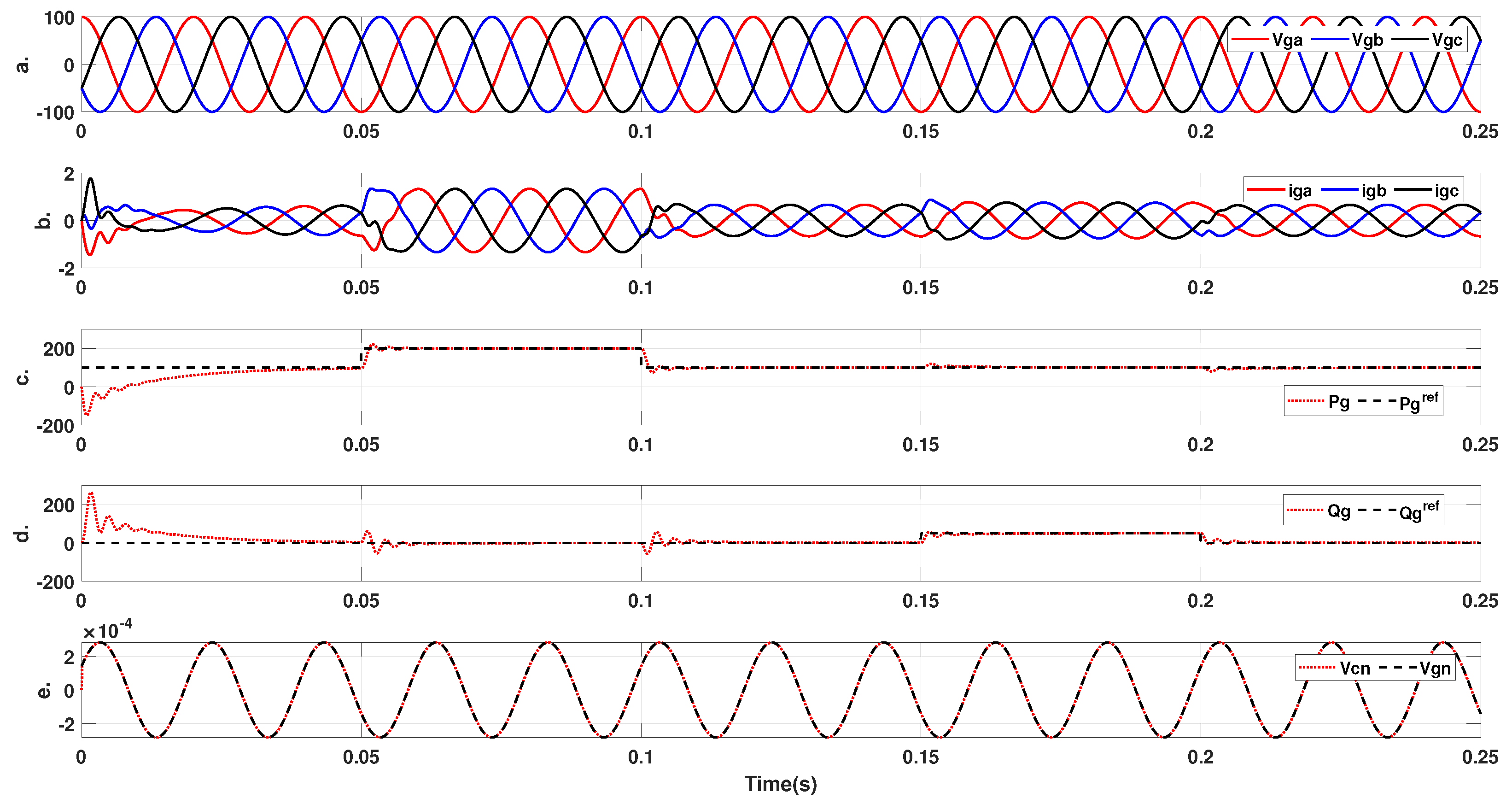
4.1. Case A: VSI Source Results with the MG in Balance Condition

The grid voltage for each phase of the balanced grid is set at 100 Volts, as seen in Figure 4a. Figure 4b depicts the respective current injections to the grid as per the requirements of active (or) and reactive powers seen in Figure 4c,d. Figure 4e shows the average voltage (or the neutral voltage) requirement of the MG and the corresponding mean voltage of the VSI source. For the symmetric or balanced grid case, the designed controller is able to keep the required mean voltage to zero at the output of the converter. It is quite evident that the designed control procedure is maintaining the desired injections of orthogonal powers to the MG, as seen in Figure 4c,d.
Further, the locus plots of the MG voltages, inverter’s output voltages and MG currents are all shown in Figure 5, which validates the hardiness of the control structure for the balanced MG circuit.
Finally, the disturbance estimation results are given in Figure 6, showing the results of the output of the controller (or the inverter’s voltage outputs), which are clearly in symmetric form as per the requirement of the balanced MG. The changes are visible around 0.05 s, 0.1 s, 0.15 s and 0.2 s since these are the instants where the power’s set-points are rendered. Figure 6c shows the respective disturbance estimations for the imbalanced MG voltage conditions.

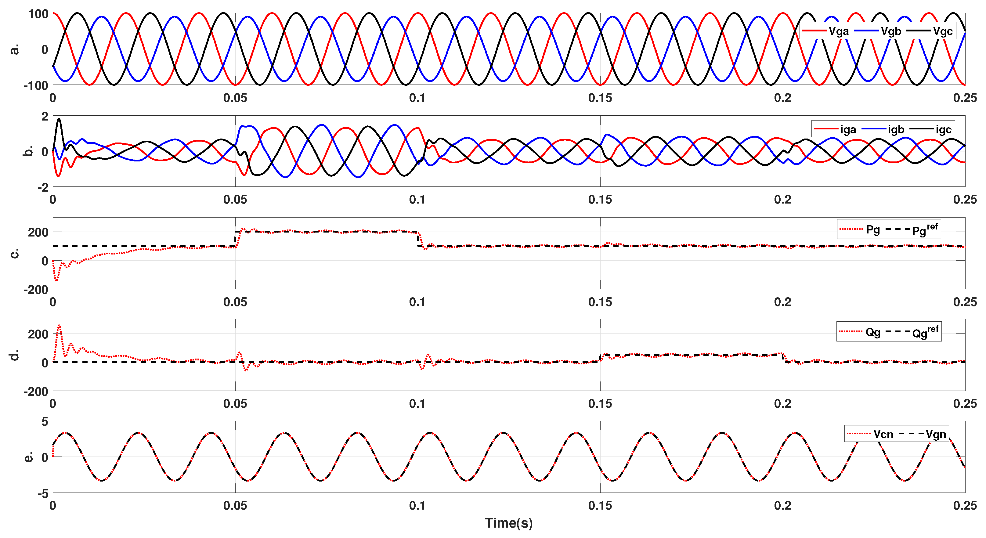
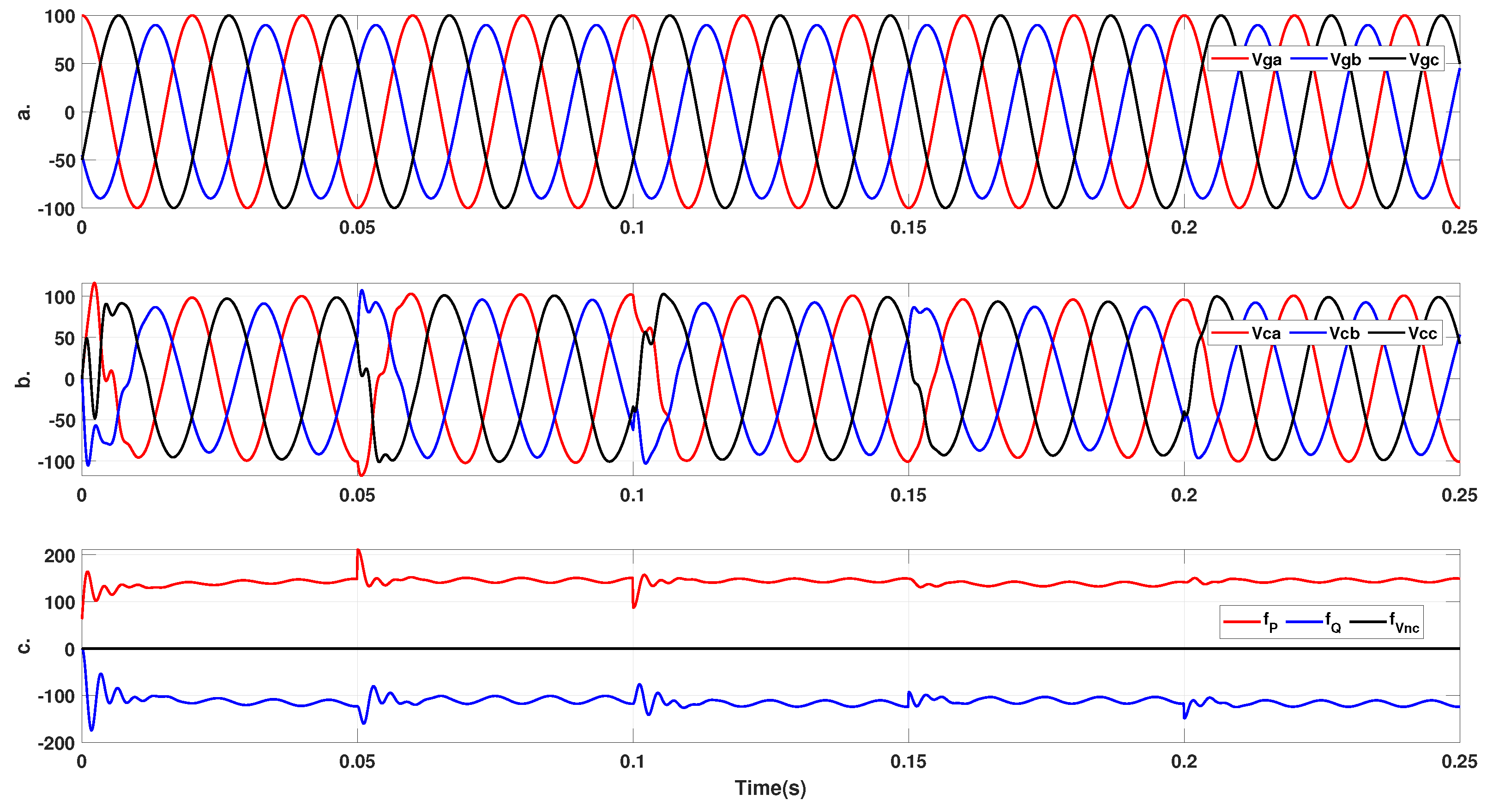
4.2. Case B: VSI Source Results with the MG in Imbalanced Condition

In the case of imbalanced MG requirements, the converter’s controlled results are given in Figure 7, Figure 8 and Figure 9. The step-wise response of the orthogonal powers and the corresponding voltages and currents of the MG are given in Figure 7. A deliberate 10% voltage reduction in phase b is introduced in the MG for the entire duration of the simulation to depict the converter’s controller response for the case of the imbalanced MG.
In Figure 7, the first row shows the imbalance grid voltages, the second row shows the corresponding grid current requirements, the third and fourth rows show the power’s step response requirements of the grid and the last row shows the corresponding average/neutral voltages, with all the average voltages displaying clearly non-zero values corresponding to the grid’s imbalance demands. During intervals 0.05–0.1 s and 0.15–0.2 s, a step variation in the reference powers (Pg, Qg) was introduced and the corresponding power injections by the three-phase inverter can be seen to be in line with the reference values, with very few oscillations compared to the balanced MG case, as in Figure 4.
The VSI source results with the imbalanced grid from Figure 7 have also been depicted by corresponding locus plots in Figure 8. The locus plots of the output voltages, the MG voltages and the MG currents all have been plotted alongside each other to highlight the efficacy of the controller’s capability to enforce the desired output voltages of the inverter, which are seen to be oval, confirming the matching with the imbalance requirements.
Finally, Figure 9 shows the results of the controller output (or the inverter’s output voltages), which are obviously imbalanced as per the requirement of the imbalanced grid. The transients can be noticed around 0.05 s, 0.1 s, 0.15 s and 0.2 s since these are the instants where the power’s set-points are rendered. Figure 9c shows the respective disturbance estimations for the imbalanced MG voltage conditions.
The values used for different parameters and control gains in the simulation are tabulated in the following Table 1.

5. Conclusions

The simulation results have proven the capability of both the proposed mathematical model of the MG-connected DG structure by augmenting the MG mean error voltage, and the relevant disturbance observer-based controller design, in the effective utilization of the full DOF of VSI under imbalanced MG voltage conditions. The proposed method has proven to be a generic method to satisfy both the symmetric and asymmetric conditions of the MG. The proposed method has successfully achieved this goal by enabling the VSI filter’s mean voltage to track the MG’s mean voltage and the switching inverter to generate output voltages to satisfy the VSI’s filter’s mean voltage. The proven controller can also be named the (P,Q,0) or (d,q,0) controller, due to mean voltage or zero sequence being part of the novel mathematical model and controller design. The results have also proven that the proposed methodology enables the three-phase inverter to generate the voltages and currents necessary to meet the required active and reactive powers at the end of the MG, irrespective of the symmetric and asymmetric MG voltage requirements. The proposed structure also works effectively irrespective of the level of disturbance, due to the DOB included as part of the control structure. The future plan is to augment the mean voltage of the MG in the MG-connected VSI model in the double synchronous frame or the model based on symmetrical components so as to explore whether it can provide even better results in terms of a fast response to imbalance requirements.

Author Contributions

Conceptualization, methodology, software simulation, formal analysis, investigation, writing—original draft preparation, writing—review and editing, A.R. and F.A.; writing—review and editing, S.A.R.K., M.S.F. and E.M.; visualization, supervision, project administration, funding acquisition, A.R. All authors have read and agreed to the published version of the manuscript.

Funding

This research received no external funding and the APC was partially funded by the University of Botswana, https://www.ub.ac.bw.

Data Availability Statement

Data sharing is not applicable to this article.

Conflicts of Interest

The authors declare no conflict of interest.

Abbreviations

The following abbreviations are used in this manuscript:
VSIVoltage Source Inverter
DGDistributed Generator
MG     Micro-Grid
SGSmart Grid
DOFDegree of Freedom
RESRenewable Energy Systems
PCCPoint of Common Coupling
PWMPulse Width Modulation
SMCSliding-Mode Control
FORFrame of Reference
RFReference Frame

References

  1. Bharothu, J.N.; Sridhar, M.; Rao, R.S. A literature survey report on Smart Grid technologies. In Proceedings of the IEEE International Conference on Smart Electric Grid (ISEG), Guntur, India, 19–20 September 2014; pp. 1–8. [Google Scholar]
  2. Ekanayake, J.B.; Jenkins, N.; Liyanage, K.; Wu, J.; Yokoyama, A. Smart grid: Technology and applications. In Smart Grid: Technology and Applications; John Wiley & Sons: Hoboken, NJ, USA, 2012. [Google Scholar]
  3. Ahmad, F.; Rasool, A.; Ozsoy, E.; Sekar, R.; Sabanovic, A.; Elitaş, M. Distribution system state estimation-A step towards smart grid. Renew. Sustain. Energy Rev. 2018, 81, 2659–2671. [Google Scholar] [CrossRef] [Green Version]
  4. Kaviri, S.M.; Pahlevani, M.; Jain, P.; Bakhshai, A. A review of AC microgrid control methods. In Proceedings of the 8th IEEE International Symposium on Power Electronics for Distributed Generation Systems (PEDG), Florianópolis, Brazil, 17–20 April 2017; pp. 1–8. [Google Scholar]
  5. Colak, I.; Kabalci, E.; Fulli, G.; Lazarou, S. A survey on the contributions of power electronics to smart grid systems. Renew. Sustain. Energy Rev. 2015, 47, 562–579. [Google Scholar] [CrossRef]
  6. Teodorescu, R.; Liserre, M.; Rodriguez, P. Grid Converters for Photovoltaic and Wind Power Systems; John Wiley & Sons: Hoboken, NJ, USA, 2011. [Google Scholar]
  7. Benysek, G.; Kazmierkowski, M.; Popczyk, J.; Strzelecki, R. Power electronic systems as a crucial part of Smart Grid infrastructure—A survey. Bull. Pol. Acad. Sci. Tech. Sci. 2011, 59, 455–473. [Google Scholar] [CrossRef] [Green Version]
  8. Arbab-Zavar, B.; Palacios-Garcia, E.J.; Vasquez, J.C.; Guerrero, J.M. Smart Inverters for Microgrid Applications: A Review. Energies 2019, 12, 840. [Google Scholar] [CrossRef] [Green Version]
  9. Jiang, H.; Cao, S.; Soh, C.B.; Wei, F. Unbalanced load modeling and control in microgrid with isolation transformer. In Proceedings of the IEEE International Conference on Electrical Drives & Power Electronics (EDPE), Dubrovnik, Croatia, 22–24 September 2021; pp. 129–135. [Google Scholar]
  10. Özsoy, E.; Padmanaban, S.; Mihet-Popa, L.; Fedák, V.; Ahmad, F.; Rasool, A.; Şabanoviç, A. Control strategy for grid connected inverters under unbalanced network conditions-A DOb based decoupled current approach. Energies 2017, 47, 562–579. [Google Scholar]
  11. Li-Jun, J.; Miao-Miao, J.; Guang-Yao, Y.; Yi-Fan, C.; Rong-Zheng, L.; Hai-Peng, Z.; Ke, Z. Unbalanced control of grid-side converter based on DSOGI-PLL. In Proceedings of the IEEE 10th Conference on Industrial Electronics and Applications (ICIEA), Auckland, New Zealand, 15–17 June 2015; pp. 1145–1149. [Google Scholar]
  12. Suul, J.A. Control of Grid Integrated Voltage Source Converters under Unbalanced Conditions: Development of an on-Line Frequency-Adaptive Virtual Flux-Based Approach. Ph.D. Thesis, Norwegian University of Science and Technology, Trondheim, Norway, 2012. [Google Scholar]
  13. Puranik, S.; Keyhani, A.; Chatterjee, A. Control of Three-Phase Inverters in Microgrid Systems. In Smart Power Grids 2011; Springer: Berlin/Heidelberg, Germany, 2012; pp. 103–176. [Google Scholar]
  14. Brod, D.M.; Novotny, D.W. Current control of VSI-PWM inverters. IEEE Trans. Ind. Appl. 1985, 3, 562–570. [Google Scholar] [CrossRef]
  15. Tenca, P.; Lipo, T.A. Synthesis of desired AC line currents in current-sourced DC-AC converters. In Proceedings of the IEEE Second International Conference on Power Electronics, Machines and Drives (PEMD), Edinburgh, UK, 31 March–2 April 2004; pp. 656–661. [Google Scholar]
  16. Milosevic, M. Decoupling control of d and q current components in three-phase voltage source inverter. In Proceedings of the IEEE Power Systems Conference and Exposition (PSCE), Atlanta, GA, USA, 29 October–1 November 2006; pp. 34–44. [Google Scholar]
  17. Sowmmiya, U.; Jamuna, V. Voltage control scheme for three phase SVM inverter fed induction motor drive systems. In Proceedings of the IEEE 1st International Conference on Electrical Energy Systems (ICEES), Chennai, India, 3–5 January 2011; pp. 207–211. [Google Scholar]
  18. Sabanovic, A.; Ohnishi, K.; Sabanovic, N. Control of PWM three phase converters: A sliding mode approach. In Proceedings of the Conference Record of Power Conversion Conference, Yokohama, Japan, 19–21 April 1993; pp. 188–193. [Google Scholar]
  19. Fiaz, A.; Rasool, A.; Ozsoy, E.E.; Sabanoviç, A.; Elitas, M. A robust cascaded controller for DC-DC Boost and Cuk converters. World J. Eng. 2017, 14, 459–466. [Google Scholar]
  20. Vijay, A.S.; Doolla, S.; Chandorkar, M. Unbalance mitigation strategies in microgrids. IET Power Electron. 2020, 13, 1687–1710. [Google Scholar] [CrossRef]
  21. Navas-Fonseca, A.; Burgos-Mellado, C.; Gómez, J.S.; Donoso, F.; Tarisciotti, L.; Saez, D.; Cardenas, R.; Sumner, M. Distributed predictive secondary control for imbalance sharing in AC microgrids. IEEE Trans. Smart Grid 2022, 13, 20–37. [Google Scholar] [CrossRef]
  22. Utkin, V.; Guldner, J.; Shi, J. Sliding Mode Control in Electro-Mechanical Systems, 3rd ed.; Taylor & Francis, CRC Press: Boca Raton, FL, USA, 2017; pp. 333–374. [Google Scholar]
  23. Wodyk, S.; Iwanski, G. Three-phase converter power control under grid imbalance with consideration of instantaneous power components limitation. Int. Trans. Electr. Energy Syst. 2020, 30, e12389. [Google Scholar] [CrossRef]
  24. Rasool, A. Control of Three Phase Converters as Source for Microgrid. Ph.D. Thesis, Sabancı University, Tuzla, Istanbul, Turkey, 2017. [Google Scholar]
Figure 1. The structure of the MG composed of DGs based on VSI [5].
Symmetry 15 00865 g001
Figure 2. Interconnecting structure of RES and the MG [24].
Symmetry 15 00865 g002
Figure 3. Novel control structure of VSI supported MG.
Symmetry 15 00865 g003
Figure 4. Power step responses of the symmetric MG connected VSI source. (a) Grid voltages ( v g [ V ] ), (b) Grid currents ( i g [ A ] ), (c) Active power ( P g [ W ] ), (d) Reactive power ( Q g [ V A R ] ), (e) Neutral/mean voltages ( v n [ V ] ).
Symmetry 15 00865 g004
Figure 5. Locus plots of Grid voltages ( v g [ V ] ), Converter output voltages ( v c [ V ] ), and Grid currents ( i g [ A ] ) for power step response with symmetric MG conditions.
Symmetry 15 00865 g005
Figure 6. Disturbance estimation results for Pg, Qg and v n c with symmetric MG. (a) Grid voltage ( v g [ V ] ), (b) VSI output voltages ( v c [ V ] ) and (c) Disturbance estimations ( f ^ P Q η [ V ] ).
Symmetry 15 00865 g006
Figure 7. Power step responses of the asymmetric MG connected VSI source. (a) Grid voltages ( v g [ V ] ), (b) Grid currents ( i g [ A ] ), (c) Active power ( P g [ W ] ), (d) Reactive power ( Q g [ V A R ] ), (e) Neutral/mean voltages ( v n [ V ] ).
Symmetry 15 00865 g007
Figure 8. Locus plots of Grid voltages ( v g [ V ] ), Converter output voltages ( v c [ V ] ), and Grid currents ( i g [ A ] ) for power step response with asymmetric MG conditions.
Symmetry 15 00865 g008
Figure 9. Disturbance estimation results for Pg, Qg and v n c with asymmetric MG. (a) Grid voltage ( v g [ V ] ), (b) VSI output voltages ( v c [ V ] ) and (c) Disturbance estimations ( f ^ P Q η [ V ] ).
Symmetry 15 00865 g009
Table 1. Parameter values and control gains for VSI-based MG.
Quantity (Symbol)Magnitude Units
Grid Voltage ( v g )100-Volts
Grid Inductance ( L g )50-mH
Filter Inductance ( L f )22-mH
Filter Capacitance ( C f )220- μ F
Grid Resistance ( R g )100-m Ω
Control Gains ( K P , K Q )55
Observer Gains (L)1200
Disclaimer/Publisher’s Note: The statements, opinions and data contained in all publications are solely those of the individual author(s) and contributor(s) and not of MDPI and/or the editor(s). MDPI and/or the editor(s) disclaim responsibility for any injury to people or property resulting from any ideas, methods, instructions or products referred to in the content.

