Article

Controlling I-V Hysteresis in Al/Pt Bilayer Symmetric SQUIDs at Millikelvin Temperatures

by
Dmitry S. Yakovlev
1,
Ivan A. Nazhestkin
2,
Nidzhat G. Ismailov
3,
Sergei V. Egorov
2,4,
Vladimir N. Antonov
5,6,* and
Vladimir L. Gurtovoi
2,7
1
Laboratoire de Physique et d’Etude des Matériaux, ESPCI-Paris, PSL Research University, 75005 Paris, France
2
Russian Quantum Center, Skolkovo, 143025 Moscow, Russia
3
Faculty of Physics, Lomonosov Moscow State University, 119991 Moscow, Russia
4
Laboratory of Superconductivity, Institute of Solid State Physics, 142432 Chernogolovka, Russia
5
Center for Engineering Physics, Skolkovo Institute of Science and Technology, Bolshoy Boul, 30, 121205 Moscow, Russia
6
Physics Department, Royal Holloway University of London, Egham TW20 0EX, UK
7
Institute of Microelectronics Technology and High Purity Materials, Russian Academy of Sciences, 142432 Chernogolovka, Russia
*
Author to whom correspondence should be addressed.
Symmetry 2023, 15(2), 550; https://doi.org/10.3390/sym15020550
Submission received: 28 December 2022 / Revised: 8 February 2023 / Accepted: 16 February 2023 / Published: 18 February 2023
(This article belongs to the Special Issue Quantum Dynamics in Josephson Junctions and Symmetry)

Abstract

:
We study operation of a superconducting quantum interference devices (SQUIDs) based on a new bilayer material. They can be used for the ultra-sensitive detection of magnetic momentum at temperatures down to milliKelvin range. Typically, thermal origin hysteresis of the symmetric SQUID current-voltage curves limits operating temperatures to T > 0.6 T c . We used a new bilayer material for SQUID fabrication, namely proximity-coupled superconductor/normal-metal (S/N) bilayers (aluminum 25 nm/platinum 5 nm). Because of the 5 nm Pt-layer, Al/Pt devices show nonhysteretic behavior in a broad temperature range from 20 mK to 0.8 K. Furthermore, the Al/Pt bilayer devices demonstrate an order of magnitude lower critical current compared to the Al devices, which decreases the screening parameter ( β L ) and improves the modulation depth of the critical current by magnetic flux. Operation at lower temperatures reduces thermal noise and increases the SQUID magnetic field resolution. Moreover, we expect strong decrease of two-level fluctuators on the surface of aluminum due to Pt-layer oxidation protection and hence significant reduction of the 1/f noise. Optimized geometry of Al/Pt symmetric SQUIDs is promising for the detection of single-electron spin flip.

Graphical Abstract

1. Introduction

The new wave of quantum technology aims to use basic principles of quantum mechanics, such as superposition or entanglement. Many of these devices operate at mK temperatures. High-sensitive detectors are key elements in the development of the mentioned technologies.
To obtain the precision sensing of quantum states, superconducting quantum interference devices (SQUIDs) can be used [1,2]. SQUIDs are known as the most sensitive magnetic sensors, theoretically capable of measuring magnetic fields so small as to detect a single electron spin-flip [2], which is useful for a wide range of applications [3]. The operation of SQUIDs is based on measuring the small fraction of the magnetic flux quanta. In recent decades, SQUIDs have been successfully used in scanning probe microscopes with a variety of different modes and designs [4,5,6,7,8]. Ultrasensitive SQUIDS are also used in qubits based on high-anisotropic molecular clusters and magnetic particles with large spins placed in the center of a SQUID loop. In these systems, the ground- and excited-quantum states are distinguished by a magnetic field; a sensitivity of 10–100 μB is required. Modern dilution refrigerators can provide base temperatures as low as 10 mK for the operation of such systems. Unfortunately, typical SQUIDs have depressed sensitivities at millikelvin temperatures due to hysteresis of current–voltage (I-V) characteristics [9,10,11]. In addition to the decrease in sensitivity, hysteresis prevents traditional SQUID read-out methods with current biases and increases the measurement times [12,13]. Hysteresis is quite common in many superconducting nano-structured systems, such as the superconductor–insulator–superconductor (SIS), superconductor–normal metal–superconductor (SNS), superconductor–ferromagnetic–superconductor (SFS), nanowire-based Josephson junctions (JJ), and JJs with topological insulators [14,15,16,17,18]. It is important to explain the origin of hysteresis and devise a way to tackle it. In recent decades, understanding the effect has substantially advanced, and several models have been proposed [19,20].
The motivation of our work is to develop the SQUID with suppressed hysteresis of the I-V characteristics down to the millikelvin temperature. An usual approach is to add a resistive shunt parallel to the Josephson junctions [21,22,23]. It solves the problem, but the shunt resistor takes up a lot of space on a chip. Moreover, it decreases the voltage modulation and, thus, decreases the signal-to-noise ratio of the SQUID-based readout. This can be overcome with techniques based on relaxation oscillations, which add additional noise compared to a classic readout system [24]. In SQUIDS with weak links, the shunt resistors lead to relaxation oscillations, and the resulting performances of such shunted SQUIDs are comparable to those of hysteretic SQUIDs [21]. The other approach is a determination of a critical current with the lock-in method [25], but it is complicated and slow compared to a simple readout. In [26], a bilayer of thick Ti (100 nm) and Au films (23 nm) was proposed to obtain a regime without hysteresis at temperatures up to mK.
As the authors of [27] show, when using materials with ρ s > ρ n (where ρ n and ρ s are the normal-state resistivity types of normal and superconducting metals, respectively), the critical currents at low temperatures increase in times of low temperatures relative to superconducting films without noble normal metal films, which apparently complicates obtaining the hysteresis-free mode, requiring a thicker film of normal metal [28].
In our work, we use a combination of materials where ρ s < < ρ n . Aluminum is used as the superconducting layer and platinum as the normal layer. With such a system, the critical current at ultra-low temperatures (down to 10 mK) is reduced and the hysteresis-free regime is preserved. Furthermore, the thin noble metal layer protects the aluminum from oxidation, leading to significant suppression of the formation of amorphous oxide on the aluminum surface and, hence, to a significant reduction in 1/f noise caused by TLS defects [29], which may bring additional advantages in ’nanoscide’ operation and a simpler condition to obtain the one-spin flip detection mode. The dominant sources of noise in SQUIDs at low temperatures are the thermal (Johnson–Nyquist) noise at the SQUID and low-frequency 1/f noise from amorphous oxides of superconducting materials (such as aluminum, niobium, and niobium nitride) on SQUID surfaces and metal-substrate interfaces [30,31,32,33]. Defects in such oxides allow atoms to tunnel between two states, resulting in the formation of two-level energy states with a wide spectral energy distribution coupled to the operating frequency range of quantum devices. As a result, amorphous oxide two-level fluctuators chaotically absorb energy from operated structures and devices, which increases the quantum detector noise, reduces the coherence time of superconducting quantum bits, and decreases the quality factors of superconducting quantum circuits [34,35].
We report SQUID based on a proximity Al/Pt (S/N) bilayer that does not have hysteresis over a wide range of cryogenic temperatures. The proximity layer pushes down T C of the constriction locale of the SQUID loop through the nearness impact and coordinates the ideal parameters with a suppressed hysteresis. Full control over the thickness of the deposition metal allows one to obtain the required critical temperature according to the Martinis equation [36]. A very important direction of the low-noise nanoSQUID realization involves the usage of oxidation-resistant superconductors, such as NbN, TiN, or MoRe [37,38,39,40,41], or protection from oxidation-noble metal-superconductor bilayers in combination with careful substrate preparation before the superconductor deposition. For our target temperature range (approximately 0.01–0.8 K), we picked Al as the superconductor (T c for the film is about 1.4 K) and Pt as the normal metal. We chose a superconductor based on the relative ease of depositing high-quality Al films. Additionally, the mesoscopic nature of electronic transport in Al has been the subject of recent intensive study, with Al being the most commonly used material for fabricating qubit circuits [42]. The normal metal, platinum, decreases the critical current and leads to the suppression of the screening parameter β L = 2 π L I c Φ 0 (L is the geometric inductance of the SQUID loop), so we have β L 1 , which increases the field sensibility of the SQUID [7].
The suppressed parameter β L is also helpful when SQUIDs are used as flux-tunable inductors in superconducting resonators. Such systems are indispensable for the research of many types of quantum systems, but a magnetic flux hysteresis in a SQUID with β L 1 , which leads to a premature switch to another resonant frequency, thus significantly reducing the resonator tuning range [43]. In addition, a reduced critical current leads to the increment of a SQUID inductance L S = Φ 0 / I C cos π Φ / Φ 0 , this can be useful in microwave readout techniques. In application to magnetometry, a resolution of 30 n Φ 0 / H z at 30 mK [44] was achieved.
The method introduced in this work allows for extending the temperature range of a SQUID without any additional limitations, such as increased noise or decreased sensitivity, which are commonly encountered with current approaches. This combination (i.e., of increased sensitivity and a low-temperature working range) paves the way toward achieving a sensitivity approaching one Bohr magneton.

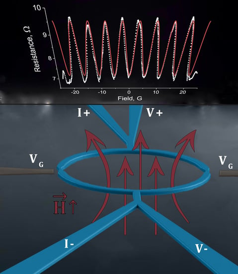
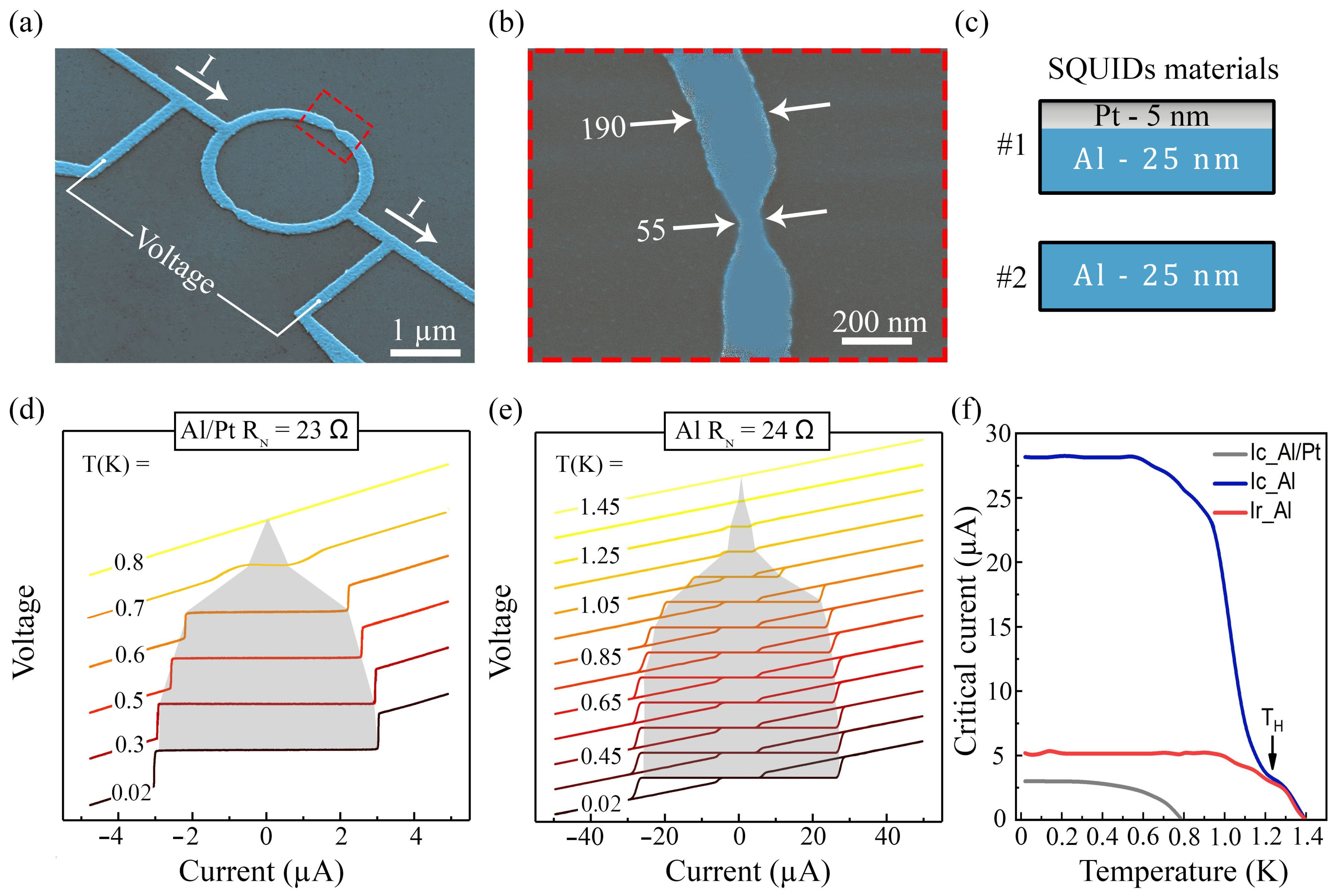
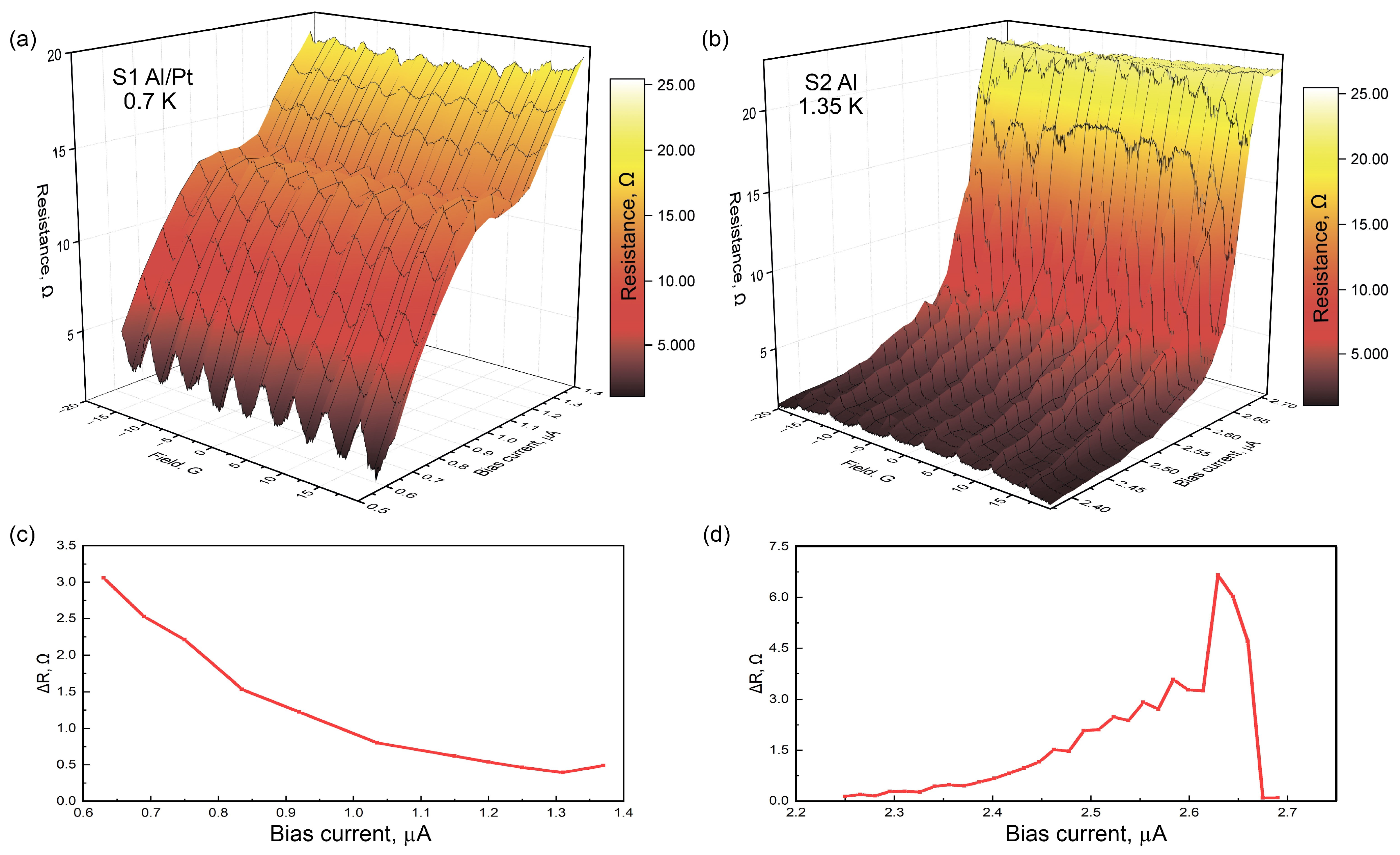
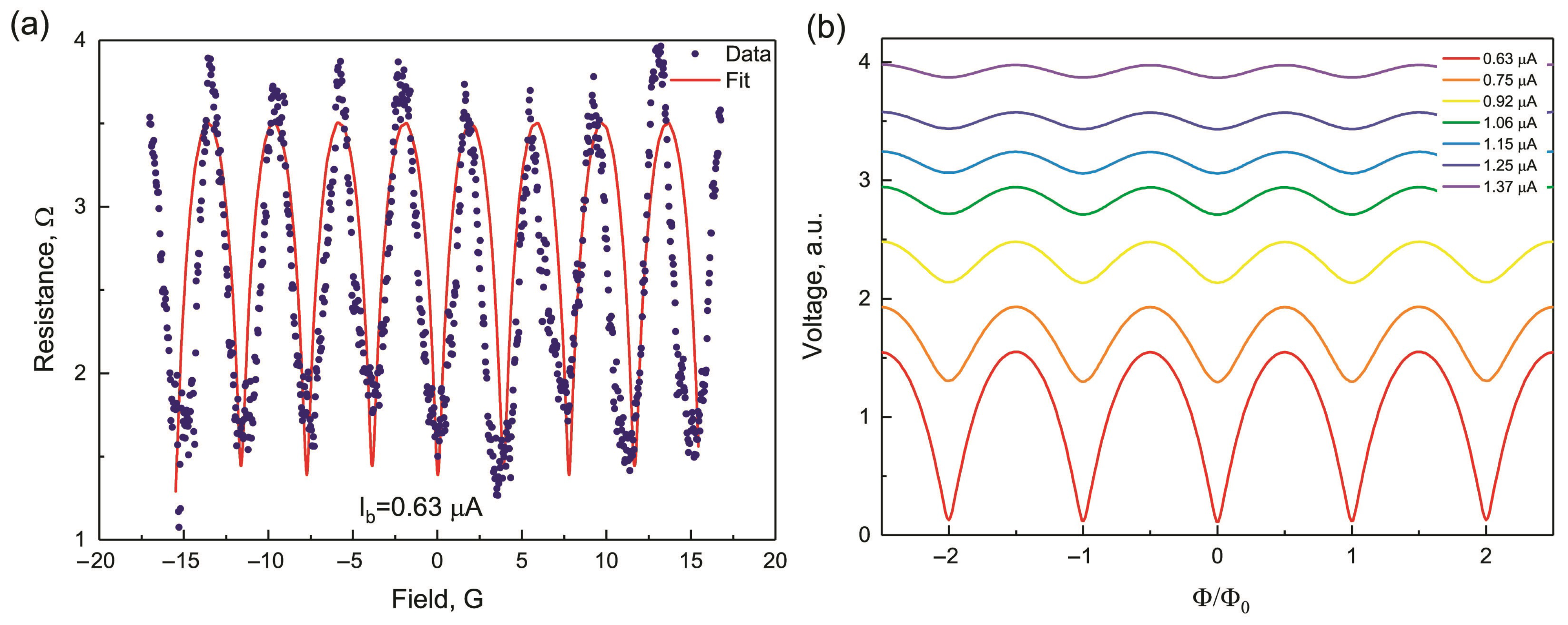
2. Results and Discussion

The device was fabricated using a standard planar technique where two constrictions (Dayem bridges) serve as weak links. We used electron beam lithography (EBL) followed by Al (25 nm) or Al (25 nm)/Pt (5 nm) deposition with electron beam evaporation on an undoped Si substrate, which was followed by a lift-off process. The platinum layer suppresses the superconducting order parameter in Al in a temperature range from 20 to 800 mK. Electrical transport measurements were conducted down to 20 mK. Further details are presented in Section 3.
The scanning electron microscopy (SEM) images of our typical fabricated SQUID are presented in Figure 1a. The Josephson junction is a constriction with lateral sizes area = 50 × 55 nm (Figure 1b). The thicknesses of the Al/Pt and Al films were 25/5 and 25 nm, respectively (Figure 1c). The SQUID loop area was 2 × 2 μ m 2 . The relevant characteristics of both devices are shown in Table 1. The electrical resistivity of a device was ρ = R N d l 2 / W + 2 l 3 / W + l / 2 W , where l 2 and l 3 are the length of a quarter of a loop and connecting wire, respectively, W is the width, and l and w are the junction length and width, respectively. This yielded 35.59 Ω · nm for Al SQUID and 40.93 Ω · nm for Al/Pt SQUID. The I–V curves of the Al/Pt SQUID at 0.02–0.8 K are shown in Figure 1d. The maximum critical current I c = 2.93 μ A was achieved at 20 mK. The curves exhibited non-hysteresis behavior in the range of 0.02–0.800 K. The I–V curves of pure Al SQUID are shown in Figure 1e. The critical current at 20 mK is 10 times larger compared to Al/Pt SQUID, I c = 28.4 μ A. The I–V curves exhibit hysteresis behavior in a wide range, from 0.02 to 1.25 K. Figure 1f shows the evolution of critical currents with temperature for both devices. For the Al sample, there is a crossover temperature between hysteresis and non-hysteresis behavior, T H 1.25 K. Thus, the Al SQUID can be used only in a narrow temperature range, from 1.25 to 1.4 K. The Al/Pt SQUIDs can be used in a much wider temperature range of 0.02–0.8 K, where they exhibit non-hysteresis behavior. It is a consequence of the small screening parameter β L in the Al/Pt sample because of the proximity effect. Next, we demonstrate the performances of our devices.
Figure 2 shows the magnetoresistance modulation of the samples taken close to the T c , at T = 0.7 K for Al/Pt SQUID and T = 1.35 K for Al SQUID at different bias currents. A magnetic field is applied as normal to the film surface. Periodic oscillations of R of the Al/Pt device are observed for a bias current between 0.5 and 1.4 μ A (Figure 2a). The period of the oscillations, δ H 5.3 G, corresponds to the magnetic flux quantum, Φ 0 = h / 2 e through the effective area of the loop. For the Al device, the magnetoresistance oscillations have parabolic shapes with minima at Φ = n Φ 0 and maxima (parabolas junctures) at Φ = n Φ 0 / 2 (see Figure 2b). The oscillation amplitudes in the Al/Pt and Al devices have different dependencies on the bias current; see Figure 2c,d. They monotonically decrease in the Al/Pt sample, while in the Al sample, they increase with a sharp jump at 2.67 μ A followed by a drop to a negligible value after a jump.
The measured and modeled magnetoresistance oscillations for the Al/Pt SQUID are presented in Figure 3. The oscillations are typical for SQUIDs [45]. They can be described with the SQUID model for I C = 0.629 μ A. We obtained a resistance modulation depth R 3 Ω for values of the bias current slightly above I C . A linear drift in the data arising from the temperature instability in a refrigerator was removed. The oscillations for the bilayer Al/Pt sample fit well with the low capacitance SQUID RSJ model [45,46] (Figure 3a) for the vast majority of Dayem bridge devices. The critical current at this temperature was a fit parameter and was used to clarify the value from a I–V curve at a temperature close to critical. The system of differential equations presented in Section 3 describes the dynamics of SQUID, as well as the average SQUID voltage. A system was solved numerically using the Adams method. Some discrepancies in amplitude presumably arise from the inequality between the critical currents of two Dayem bridges. Figure 3b shows changes in the shape of the magnetoresistance curve at different bias currents i b = I b / I c . Note the periodic behaviors of flux quanta, provided that the SQUID is single-valued. See Section 3 for calculation details. Our measurement results show that non-hysteretic SQUID can be considered as a magnetic flux to the voltage transducer and can be employed as a good magnetic flux detector.
The hysteresis in SQUIDs is usually referred to as the Joule heating effect at the weak link regions [9]. For single-layer Al cases, the large hysteresis appeared when the current exceeded 20 μ A. At the same time, in Al/Pt bilayer SQUIDs, the hysteresis at this current was not observed. The tolerance to the self-heating effect was improved by the bilayer structure. These facts indicate that the presence of a normal layer, particularly the Pt layer, effectively reduces the heat concentration at the junction area. This method with a normal metal layer used as a thermal shunt has already been used in devices with higher bath temperatures [47,48]. We pioneered the application of a thermal shunt at ultralow temperatures.
We observed an atypical dependence of the critical current I c on the temperature, which cannot be explained within standard theories. In Dayem bridges, suppression of superconductivity can result from the motion of Abrikosov vortices across a junction or the occurrence of phase-slip centers originating from thermal or quantum fluctuations [49,50]. The size of the vortex in the latter case is about ξ . In thin films, Al is in the dirty limit and ξ A l = D 2 π k B T C [51], where D is a diffusion constant. Using the Einstein relation σ = e 2 N D , where N = 2.4 × 10 28 eV 1 cm 1 is the density of Al states at the Fermi energy [52,53], one can find D = 7.18 and ξ A l = 78.7 nm, which is more than a junction width of 55 nm. Consequently, the specificity of a critical current dependence can be explained by phase-slip centers. At these points, quantum fluctuations produce stochastic variations of the critical current around an average value. A resulting stable normal or superconductive state depends on the state times, which in turn are determined by junction voltage.

3. Methods

3.1. E-Beam Lithography and Deposition

A high-resolution electron beam (e-beam) lithography system was exploited for nano-patterning the films. We used poly(methyl methacrylate) (PMMA) as a positive tone resist. To pattern the masks, we used a JEOL 7001f SEM equipped with an EBL module. The necessary dose in our case was 400 μ C/cm 2 . We used a mixture of MIBK 1 part and IPA 3 parts to develop the e-beam pattern and clean IPA as a stopper. After development, the mask was dried in N 2 gas.
We used the e-beam evaporation technique through a tough mask and the controlled lift-off process. Fabrication consisted of three steps in one vacuum cycle e-beam evaporation at room temperature. First, etching was done by inflating a low flow of pure Argon plasma into the chamber; this involved the Ar pressure 4 × 10 3 , RF power P R F = 200 W, V D C = 250 V, Time = 10 s, and flow = 4 SCCM. Second, the e-beam evaporation of 25 nm aluminum was performed with a base pressure of 4.2 × 10 3 mBar, deposition rate of 0.5 nm/s, and emission current of 157 mA. We used 99.99% purity Al granules. Finally, 5 nm of platinum evaporation (by the e-beam) was produced with a base pressure of 7.8 × 10 8 mBar, a deposition rate of 0.2 nm/s, and an emission current of 196 mA. Because this growth was not performed on an epitaxial substrate, X-ray diffraction (XRD) measurements characterized the films as polycrystalline.

3.2. Measurement Details

All DC measurements were made in a dilution refrigerator (BlueFors LD-250). A copper sample holder carefully shielded from magnetic fields with the Amumetal shield (hydrogen annealed for maximum permeability) and from non-equilibrium photons enabled the four-point (contact) method using separate twisted pairs for current and voltage contacts. DC measurements were performed with symmetric current biasing of a sample. To minimize the switching noise of the analog-to-digital conversion (ADC) card inputs, the Leonardo II 24-bit ADC card measures signals—not from the samples directly but from the outputs of the current (AD8220) and voltage (AD8421) instrumentation amplifiers (IAs). The voltage noise density of the amplifier was 3 n V / H z . To improve the accuracy of the current signal, the voltage drop in the measured structure was removed from the current signal. All electrical inputs and outputs from the cryostat go through pi filters (C = 2.5 nF), and then through a two-stage symmetric low-pass RC filter (R = 1 k Ω , C = 100 nF, cutoff frequency of 1.7 kHz). At the 100 mK flange, a compact silver-epoxy microwave filter made of twelve 1.6 m long twisted pairs (TP filter) is used. This filter is analogous to the silver-epoxy microwave filters and ’thermalizers’ used for millikelvin experiments [54]. The TP filter is located at the input to the sample holder on the mixing chamber flange. This filter provides significant attenuation of frequencies that cannot be suppressed with RC filters (up to 20 GHz). The measuring scheme is described in detail in [55].

3.3. Magnetoresistance Oscillation Fitting

Magnetoresistance oscillations in Al/Pt SQUID were modeled using the modified resistively shunted junction model (RSJ model) [45,46]. Equations for the junction current in this approach can be written as:
I S 1 , 2 = I c sin φ 1 , 2 , I D 1 , 2 = C J d V 1 , 2 d t , I R 1 , 2 = V 1 , 2 R J , I 1 , 2 = I S 1 , 2 + I D 1 , 2 + I R 1 , 2 ,
where C J and R J are the capacitance and resistance of each junction, and I C is a junction critical current. Using the Josephson relation V = 2 e φ ˙ , the considered current can be written as:
I 1 , 2 = C J 2 e d 2 φ 1 , 2 d t 2 + 2 e R J d φ 1 , 2 d t + I c sin φ 1 , 2
One can neglect the capacitive term because of the small capacitance of Dayem bridges:
I 1 , 2 = 2 e R J d φ 1 , 2 d t + I c sin φ 1 , 2
For the whole SQUID, one can write:
I bias = I 1 + I 2 Φ = Φ e L 1 I 1 + L 2 I 2
where I bias is the SQUID bias current, I 1 and I 2 are the currents over the SQUID arms, L 1 and L 2 are the inductance of the SQUID arms, and Φ e is the external magnetic flux applied to the SQUID. After the substitution of junction currents, this system looks as follows:
I bias = I 1 + I 2 Φ = Φ e L 1 ω c 2 e R J d φ 1 d τ + I c sin φ 1 + L 2 ω c 2 e R J d φ 2 d τ + I c sin φ 2
Substitutions t = τ ω c (where ω c = 2 e I c R J ), β L 1 = L 1 L J , β L 2 = L 2 L J (where L J = 2 e I c ), make these equations dimensionless, i.e.:
i bias = φ ˙ 1 + sin φ 1 + φ ˙ 2 + sin φ 2 φ 1 φ 2 = φ e β L 1 φ ˙ 1 + sin φ 1 + β L 2 φ ˙ 2 + sin φ 2
or
φ ˙ 1 = β L 2 β L 1 + β L 2 i b 1 β L 2 φ 1 φ 2 φ e sin φ 1 φ ˙ 2 = β L 1 β L 1 + β L 2 i b + 1 β L 1 φ 1 φ 2 φ e sin φ 2
The resulting curves are presented in the main text.

4. Conclusions

In summary, we studied the temperature dependence of the critical current and magnetoresistance modulation in two different kinds symmetric SQUIDs with Dayem bridges: (1) based on aluminum and (2) on aluminum-platinum S-N bilayer. We demonstrated non-hysteresis SQUIDs capable of performing continuous read-outs down to the lowest temperature (20 mK). This makes it possible to measure the characteristics of a wide variety of modern quantum systems and decrease the temperature noise. Furthermore, the normal metal layer added to the SQUID reduces its critical current, which increases a field sensibility of a SQUID and provides an opportunity for novel applications. The potential of S-N symmetric bilayer SQUIDs to work in a continuous way at such low temperatures makes them useful tools for studying the ground-state properties of quantum systems. This design is promising for the plausible construction of a long-desired device with a single Bohr magnetron resolution. More experiments are required to fabricate different SQUIDs with variations in the thicknesses of normal and superconducting metals.

Author Contributions

V.L.G. conceived the experiment. D.S.Y. and S.V.E. fabricated the samples. D.S.Y., V.L.G. and I.A.N. performed the experiments. D.S.Y., I.A.N. and N.G.I. analyzed the data. D.S.Y., I.A.N., N.G.I. and V.N.A. wrote the manuscript with input from all authors. All authors equally discussed the results and their implications. All authors have read and agreed to the published version of the manuscript.

Funding

The work of I.A.N, S.V.E., and V.L.G. was supported by Rosatom in the framework of the Roadmap for Quantum computing (contract no. 868-1.3-15/15-2021 dated 5 October 2021).

Data Availability Statement

The data presented in this study are available upon request from the corresponding author.

Conflicts of Interest

The authors declare no conflict of interest.

References

  1. Clarke, J. SQUID fundamentals. In SQUID Sensors: Fundamentals, Fabrication and Applications; Springer: Dordrecht, The Netherlands, 1996; pp. 1–62. [Google Scholar]
  2. Anahory, Y.; Naren, H.; Lachman, E.; Sinai, S.B.; Uri, A.; Embon, L.; Yaakobi, E.; Myasoedov, Y.; Huber, M.; Klajn, R.; et al. SQUID-on-tip with single-electron spin sensitivity for high-field and ultra-low temperature nanomagnetic imaging. Nanoscale 2020, 12, 3174–3182. [Google Scholar] [CrossRef] [PubMed]
  3. Granata, C.; Vettoliere, A.; Walke, P.; Esposito, E.; Nappi, C.; Silvestrini, P.; Ruggiero, B.; Russo, M. NANO-SQUIDs based on niobium Dayem bridges for nanoscale applications. In Journal of Physics: Conference Series; IOP Publishing: Bristol, UK, 2010; Volume 234, p. 042010. [Google Scholar]
  4. Josephs-Franks, P.; Hao, L.; Tzalenchuk, A.; Davies, J.; Kazakova, O.; Gallop, J.; Brown, L.; Macfarlane, J. Measurement of the spatial sensitivity of miniature SQUIDs using magnetic-tipped STM. Supercond. Sci. Technol. 2003, 16, 1570. [Google Scholar] [CrossRef] [Green Version]
  5. Huber, M.E.; Koshnick, N.C.; Bluhm, H.; Archuleta, L.J.; Azua, T.; Björnsson, P.G.; Gardner, B.W.; Halloran, S.T.; Lucero, E.A.; Moler, K.A. Gradiometric micro-SQUID susceptometer for scanning measurements of mesoscopic samples. Rev. Sci. Instrum. 2008, 79, 053704. [Google Scholar] [CrossRef] [PubMed]
  6. Bouchiat, V. Detection of magnetic moments using a nano-SQUID: Limits of resolution and sensitivity in near-field SQUID magnetometry. Supercond. Sci. Technol. 2009, 22, 064002. [Google Scholar] [CrossRef]
  7. Granata, C.; Vettoliere, A. Nano superconducting quantum interference device: A powerful tool for nanoscale investigations. Phys. Rep. 2016, 614, 1–69. [Google Scholar] [CrossRef] [Green Version]
  8. Kudriashov, A.; Babich, I.; Hovhannisyan, R.A.; Shishkin, A.G.; Kozlov, S.N.; Fedorov, A.; Vyalikh, D.V.; Khestanova, E.; Kupriyanov, M.Y.; Stolyarov, V.S. Revealing Intrinsic Superconductivity of the Nb/BiSbTe2Se Interface. Adv. Funct. Mater. 2022, 32, 2209853. [Google Scholar] [CrossRef]
  9. Hazra, D.; Pascal, L.M.; Courtois, H.; Gupta, A.K. Hysteresis in superconducting short weak links and μ-SQUIDs. Phys. Rev. B 2010, 82, 184530. [Google Scholar] [CrossRef] [Green Version]
  10. Keijers, W.; Baumans, X.D.; Panghotra, R.; Lombardo, J.; Zharinov, V.S.; Kramer, R.B.; Silhanek, A.V.; Van de Vondel, J. Nano-SQUIDs with controllable weak links created via current-induced atom migration. Nanoscale 2018, 10, 21475–21482. [Google Scholar] [CrossRef]
  11. Ishiguro, R.; Watanabe, E.; Sakuma, D.; Shinozaki, T.; Tsuchiya, S.; Nago, Y.; Osato, H.; Tsuya, D.; Kashiwaya, H.; Kashiwaya, S.; et al. Development of nano and micro SQUIDs based on Al tunnel junctions. In Journal of Physics: Conference Series; IOP Publishing: Bristol, UK, 2014; Volume 568, p. 022019. [Google Scholar]
  12. Gallop, J. SQUIDs: Some limits to measurement. Supercond. Sci. Technol. 2003, 16, 1575. [Google Scholar] [CrossRef]
  13. Wernsdorfer, W. From micro-to nano-SQUIDs: Applications to nanomagnetism. Supercond. Sci. Technol. 2009, 22, 064013. [Google Scholar] [CrossRef]
  14. Golikova, T.E.; Wolf, M.J.; Beckmann, D.; Penzyakov, G.A.; Batov, I.E.; Bobkova, I.; Bobkov, A.M.; Ryazanov, V.V. Controllable supercurrent in mesoscopic superconductor-normal metal-ferromagnetcrosslike Josephson structures. Supercond. Sci. Technol. 2021, 34, 095001. [Google Scholar] [CrossRef]
  15. Frielinghaus, R.; Batov, I.; Weides, M.; Kohlstedt, H.; Calarco, R.; Schäpers, T. Josephson supercurrent in Nb/InN-nanowire/Nb junctions. Appl. Phys. Lett. 2010, 96, 132504. [Google Scholar] [CrossRef] [Green Version]
  16. Yakovlev, D.S.; Lvov, D.S.; Emelyanova, O.V.; Dzhumaev, P.S.; Shchetinin, I.V.; Skryabina, O.V.; Egorov, S.V.; Ryazanov, V.V.; Golubov, A.A.; Roditchev, D.; et al. Physical Vapor Deposition Features of Ultrathin Nanocrystals of Bi2 (Te x Se1–x) 3. J. Phys. Chem. Lett. 2022, 13, 9221–9231. [Google Scholar] [CrossRef] [PubMed]
  17. Sotnichuk, S.V.; Skryabina, O.V.; Shishkin, A.G.; Bakurskiy, S.V.; Kupriyanov, M.Y.; Stolyarov, V.S.; Napolskii, K.S. Long Single Au Nanowires in Nb/Au/Nb Josephson Junctions: Implications for Superconducting Microelectronics. ACS Appl. Nano Mater. 2022, 5, 17059–17066. [Google Scholar] [CrossRef]
  18. Karelina, L.; Hovhannisyan, R.A.; Golovchanskiy, I.; Chichkov, V.; Ben Hamida, A.; Stolyarov, V.; Uspenskaya, L.; Erkenov, S.A.; Bolginov, V.; Ryazanov, V. Scalable memory elements based on rectangular SIsFS junctions. J. Appl. Phys. 2021, 130, 173901. [Google Scholar] [CrossRef]
  19. Angers, L.; Chiodi, F.; Montambaux, G.; Ferrier, M.; Guéron, S.; Bouchiat, H.; Cuevas, J. Proximity dc squids in the long-junction limit. Phys. Rev. B 2008, 77, 165408. [Google Scholar] [CrossRef] [Green Version]
  20. Courtois, H.; Meschke, M.; Peltonen, J.; Pekola, J.P. Origin of hysteresis in a proximity Josephson junction. Phys. Rev. Lett. 2008, 101, 067002. [Google Scholar] [CrossRef] [Green Version]
  21. Kumar, N.; Winkelmann, C.; Biswas, S.; Courtois, H.; Gupta, A.K. Controlling hysteresis in superconducting constrictions with a resistive shunt. Supercond. Sci. Technol. 2015, 28, 072003. [Google Scholar] [CrossRef] [Green Version]
  22. Foglietti, V.; Gallagher, W.; Ketchen, M.; Kleinsasser, A.; Koch, R.; Sandstrom, R. Performance of dc SQUIDs with resistively shunted inductance. Appl. Phys. Lett. 1989, 55, 1451–1453. [Google Scholar] [CrossRef]
  23. Nagel, J.; Konovalenko, K.; Kemmler, M.; Turad, M.; Werner, R.; Kleisz, E.; Menzel, S.; Klingeler, R.; Büchner, B.; Kleiner, R.; et al. Resistively shunted YBa2Cu3O7 grain boundary junctions and low-noise SQUIDs patterned by a focused ion beam down to 80 nm linewidth. Supercond. Sci. Technol. 2010, 24, 015015. [Google Scholar] [CrossRef] [Green Version]
  24. Muck, M.; Heiden, C. Simple DC-SQUID system based on a frequency modulated relaxation oscillator. IEEE Trans. Magn. 1989, 25, 1151–1153. [Google Scholar] [CrossRef]
  25. Hovhannisyan, R.A.; Kapran, O.M.; Golod, T.; Krasnov, V.M. Accurate Determination of the Josephson Critical Current by Lock-In Measurements. Nanomaterials 2021, 11, 2058. [Google Scholar] [CrossRef] [PubMed]
  26. Blois, A.; Rozhko, S.; Hao, L.; Gallop, J.; Romans, E. Proximity effect bilayer nano superconducting quantum interference devices for millikelvin magnetometry. J. Appl. Phys. 2013, 114, 233907. [Google Scholar] [CrossRef]
  27. Vodolazov, D.Y.; Aladyshkin, A.Y.; Pestov, E.; Vdovichev, S.; Ustavshikov, S.; Levichev, M.Y.; Putilov, A.; Yunin, P.; El’kina, A.; Bukharov, N.; et al. Peculiar superconducting properties of a thin film superconductor–normal metal bilayer with large ratio of resistivities. Supercond. Sci. Technol. 2018, 31, 115004. [Google Scholar] [CrossRef]
  28. Blois, A.; Rozhko, S.; Hao, L.; Gallop, J.; Romans, E. Heat propagation models for superconducting nanobridges at millikelvin temperatures. Supercond. Sci. Technol. 2016, 30, 014003. [Google Scholar] [CrossRef]
  29. Burnett, J.; Faoro, L.; Wisby, I.; Gurtovoi, V.; Chernykh, A.; Mikhailov, G.; Tulin, V.; Shaikhaidarov, R.; Antonov, V.; Meeson, P.; et al. Evidence for interacting two-level systems from the 1/f noise of a superconducting resonator. Nat. Commun. 2014, 5, 1–6. [Google Scholar] [CrossRef] [Green Version]
  30. Barone, C.; Rotzinger, H.; Voss, J.N.; Mauro, C.; Schön, Y.; Ustinov, A.V.; Pagano, S. Current-resistance effects inducing nonlinear fluctuation mechanisms in granular aluminum oxide nanowires. Nanomaterials 2020, 10, 524. [Google Scholar] [CrossRef] [Green Version]
  31. Burin, A.L.; Matityahu, S.; Schechter, M. Low-temperature 1/f noise in microwave dielectric constant of amorphous dielectrics in Josephson qubits. Phys. Rev. B 2015, 92, 174201. [Google Scholar] [CrossRef] [Green Version]
  32. Sofer, Z.; Shaulov, A.; Yeshurun, Y. Current dependence of the negative magnetoresistance in superconducting NbN nanowires. Sci. Rep. 2022, 12, 22027. [Google Scholar] [CrossRef]
  33. Jouan, A.; Hurand, S.; Singh, G.; Lesne, E.; Barthélémy, A.; Bibes, M.; Ulysse, C.; Saiz, G.; Feuillet-Palma, C.; Lesueur, J.; et al. Multiband Effects in the Superconducting Phase Diagram of Oxide Interfaces. Adv. Mater. Interfaces 2022, 9, 2201392. [Google Scholar] [CrossRef]
  34. Müller, C.; Lisenfeld, J.; Shnirman, A.; Poletto, S. Interacting two-level defects as sources of fluctuating high-frequency noise in superconducting circuits. Phys. Rev. B 2015, 92, 035442. [Google Scholar] [CrossRef] [Green Version]
  35. Bilmes, A.; Zanker, S.; Heimes, A.; Marthaler, M.; Schön, G.; Weiss, G.; Ustinov, A.V.; Lisenfeld, J. Electronic decoherence of two-level systems in a Josephson junction. Phys. Rev. B 2017, 96, 064504. [Google Scholar] [CrossRef] [Green Version]
  36. Martinis, J.M.; Hilton, G.C.; Irwin, K.D.; Wollman, D.A. Calculation of TC in a normal-superconductor bilayer using the microscopic-based Usadel theory. Nucl. Instrum. Methods Phys. Res. Sect. 2000, 444, 23–27. [Google Scholar] [CrossRef]
  37. Holzman, I.; Ivry, Y. On-chip integrable planar NbN nanoSQUID with broad temperature and magnetic-field operation range. AIP Adv. 2019, 9, 105028. [Google Scholar] [CrossRef] [Green Version]
  38. Russo, R.; Esposito, E.; Crescitelli, A.; Di Gennaro, E.; Granata, C.; Vettoliere, A.; Cristiano, R.; Lisitskiy, M. NanoSQUIDs based on niobium nitride films. Supercond. Sci. Technol. 2016, 30, 024009. [Google Scholar] [CrossRef]
  39. Faley, M.; Fiadziushkin, H.; Frohn, B.; Schüffelgen, P.; Dunin-Borkowski, R. TiN nanobridge Josephson junctions and nanoSQUIDs on SiN-buffered Si. Supercond. Sci. Technol. 2022, 35, 065001. [Google Scholar] [CrossRef]
  40. Faley, M.I.; Liu, Y.; Dunin-Borkowski, R.E. Titanium nitride as a new prospective material for nanoSQUIDS and superconducting nanobridge electronics. Nanomaterials 2021, 11, 466. [Google Scholar] [CrossRef] [PubMed]
  41. Shishkin, A.; Skryabina, O.; Gurtovoi, V.; Dizhur, S.; Faley, M.; Golubov, A.; Stolyarov, V. Planar MoRe-based direct current nanoSQUID. Supercond. Sci. Technol. 2020, 33, 065005. [Google Scholar] [CrossRef]
  42. Rigetti, C.; Gambetta, J.M.; Poletto, S.; Plourde, B.; Chow, J.M.; Córcoles, A.; Smolin, J.A.; Merkel, S.T.; Rozen, J.; Keefe, G.A.; et al. Superconducting qubit in a waveguide cavity with a coherence time approaching 0.1 ms. Phys. Rev. B 2012, 86, 100506. [Google Scholar] [CrossRef] [Green Version]
  43. Kennedy, O.; Burnett, J.; Fenton, J.; Constantino, N.; Warburton, P.; Morton, J.; Dupont-Ferrier, E. Tunable Nb superconducting resonator based on a constriction nano-SQUID fabricated with a Ne focused ion beam. Phys. Rev. Appl. 2019, 11, 014006. [Google Scholar] [CrossRef] [Green Version]
  44. Levenson-Falk, E.; Vijay, R.; Antler, N.; Siddiqi, I. A dispersive nanoSQUID magnetometer for ultra-low noise, high bandwidth flux detection. Supercond. Sci. Technol. 2013, 26, 055015. [Google Scholar] [CrossRef] [Green Version]
  45. Tesche, C.D.; Clarke, J. DC SQUID: Noise and optimization. J. Low Temp. Phys. 1977, 29, 301–331. [Google Scholar] [CrossRef] [Green Version]
  46. Soloviev, I.; Klenov, N.; Schegolev, A.; Bakurskiy, S.; Kupriyanov, M.Y. Analytical derivation of DC SQUID response. Supercond. Sci. Technol. 2016, 29, 094005. [Google Scholar] [CrossRef] [Green Version]
  47. Lam, S.K.; Clem, J.R.; Yang, W. A nanoscale SQUID operating at high magnetic fields. Nanotechnology 2011, 22, 455501. [Google Scholar] [CrossRef] [PubMed]
  48. Hao, L.; Macfarlane, J.; Gallop, J.; Cox, D.; Beyer, J.; Drung, D.; Schurig, T. Measurement and noise performance of nano-superconducting-quantum-interference devices fabricated by focused ion beam. Appl. Phys. Lett. 2008, 92, 192507. [Google Scholar] [CrossRef] [Green Version]
  49. Dausy, H.; Nulens, L.; Raes, B.; Van Bael, M.J.; Van de Vondel, J. Impact of Kinetic Inductance on the Critical-Current Oscillations of Nanobridge SQUIDs. Phys. Rev. Appl. 2021, 16, 024013. [Google Scholar] [CrossRef]
  50. Aref, T.; Levchenko, A.; Vakaryuk, V.; Bezryadin, A. Quantitative analysis of quantum phase slips in superconducting Mo76Ge24 nanowires revealed by switching-current statistics. Phys. Rev. B 2012, 86, 024507. [Google Scholar] [CrossRef] [Green Version]
  51. Vijay, R.; Levenson-Falk, E.; Slichter, D.; Siddiqi, I. Approaching ideal weak link behavior with three dimensional aluminum nanobridges. Appl. Phys. Lett. 2010, 96, 223112. [Google Scholar] [CrossRef] [Green Version]
  52. Poli, N.; Morten, J.P.; Urech, M.; Brataas, A.; Haviland, D.B.; Korenivski, V. Spin injection and relaxation in a mesoscopic superconductor. Phys. Rev. Lett. 2008, 100, 136601. [Google Scholar] [CrossRef] [Green Version]
  53. Jedema, F.; Heersche, H.; Filip, A.; Baselmans, J.; Van Wees, B. Electrical detection of spin precession in a metallic mesoscopic spin valve. Nature 2002, 416, 713–716. [Google Scholar] [CrossRef]
  54. Scheller, C.P.; Heizmann, S.; Bedner, K.; Giss, D.; Meschke, M.; Zumbühl, D.M.; Zimmerman, J.D.; Gossard, A.C. Silver-epoxy microwave filters and thermalizers for millikelvin experiments. Appl. Phys. Lett. 2014, 104, 211106. [Google Scholar] [CrossRef] [Green Version]
  55. Stolyarov, V.S.; Roditchev, D.; Gurtovoi, V.L.; Kozlov, S.N.; Yakovlev, D.S.; Skryabina, O.V.; Vinokur, V.M.; Golubov, A.A. Resonant Oscillations of Josephson Current in Nb-Bi2Te2. 3Se0. 7-Nb Junctions. Adv. Quantum Technol. 2022, 5, 2100124. [Google Scholar] [CrossRef]
Figure 1. Josephson transport through planar-thin Al/Pt and Al SQUID operations at various temperatures. (a) Scanning electron microscope picture of the device. The voltage across the SQUID is measured at constant I b i a s . (b) An image of constriction of 50 × 50 nm. (c) Two types of films form the SQUID, Al and Al/Pt. (d) The non-hysteresis V(I) characteristics of the Al/Pt S1 SQUID taken at T = 0.02–0.8 K. Al/Pt devices have non-hysteresis behavior at all temperature ranges. (e) The hysteresis behaviors of the Al S2 SQUIDs at different temperatures, T = 0.02–1.4 K. (f) The dependencies of the critical and re-trapping currents as functions of T. Al SQUID hysteresis occurs at T < T H = 1.25 K.
Symmetry 15 00550 g001
Figure 2. Comparison of the measured Al/Pt and Al magnetoresistance oscillations. (a,b) Resistance of Al and Al/Pt samples vs. the applied magnetic field and bias current. (c,d) The amplitude of the oscillations, Δ R vs. bias current defined at low fields.
Symmetry 15 00550 g002
Figure 3. Magnetoresistance oscillations in Al/Pt SQUID with bias current. (a) Al/Pt sample oscillations are described by the RSJ SQUID model. Blue curve: measured magnetoresistance; red curve: theoretical magnetoresistance. Oscillation period: 4.77 G. (b) Theoretical calculations for voltage modulations of SQUID as functions of the magnetic flux for different values of the bias current. The curves correspond from the bottom to the top to the applied control currents of 0.63, 0.75, 0.92, 1.06, 1.25, and 1.37 μ A, respectively.
Symmetry 15 00550 g003
Table 1. Relevant parameters of the devices.
Sample I c , μ A R n exp , Ω W constriction , nm d, nmL, nm δ H , G A eff , μ m 2 T c , K ρ n , Ω · nm
Al/Pt2.932355 ± 230 ± 150 ± 105.33.80.840.93
Al28.42452 ± 225 ± 350 ± 104.794.31.4135.59
Disclaimer/Publisher’s Note: The statements, opinions and data contained in all publications are solely those of the individual author(s) and contributor(s) and not of MDPI and/or the editor(s). MDPI and/or the editor(s) disclaim responsibility for any injury to people or property resulting from any ideas, methods, instructions or products referred to in the content.

