Article

Percolative, Multifractal, and Symmetry Properties of the Surface at Nanoscale of Cu-Ni Bimetallic Thin Films Deposited by RF-PECVD

by
Robert S. Matos
1,
Nilson S. Ferreira
2,
Ştefan Ţălu
3,*,
Atefeh Ghaderi
4,
Shahram Solaymani
4,
Marcelo A. Pires
5,
Edgar Aparecido Sanches
6 and
Henrique D. da Fonseca Filho
7,*
1
Postgraduate Program in Materials Science and Engineering, Federal University of Sergipe, São Cristovão 49100-000, SE, Brazil
2
Laboratory of Corrosion and Nanotechnology (LCNT), Federal University of Sergipe, São Cristovão 49100-000, SE, Brazil
3
The Directorate of Research, Development and Innovation Management (DMCDI), Technical University of Cluj-Napoca, Constantin Daicoviciu St., no. 15, 400020 Cluj-Napoca, Romania
4
Quantum Technologies Research Center (QTRC), Science and Research Branch, Islamic Azad University, Tehran 1477893855, Iran
5
Physics Department, Federal University of Alagoas (UFAL), Delmiro Gouveia 57480-000, AL, Brazil
6
Laboratory of Nanostructured Polymers (NANOPOL), Physics Department, Federal University of Amazonas, Manaus 69077-000, AM, Brazil
7
Laboratory of Synthesis of Nanomaterials and Nanoscopy (LSNN), Physics Department, Federal University of Amazonas, Manaus 69077-000, AM, Brazil
*
Authors to whom correspondence should be addressed.
Symmetry 2022, 14(12), 2675; https://doi.org/10.3390/sym14122675
Submission received: 12 October 2022 / Revised: 2 December 2022 / Accepted: 11 December 2022 / Published: 17 December 2022
(This article belongs to the Section Chemistry: Symmetry/Asymmetry)

Abstract

:
We explored the morphological and 3D spatial properties of Cu/Ni thin films obtained by a co-deposition process. The 3D AFM topographic maps analysis indicated that the films displayed different morphologies and rough profiles dictated by their singular directional inhomogeneities. Moreover, Minkowski’s volume showed that the Cu/Ni films deposited after 15 and 20 min had a similar relative distribution of matter as a function of height, which is different from the individual Cu films. The Minkowski boundary and connectivity point out that the percolative properties of the Cu/Ni samples were similar to each other. However, they were distinct from the percolative features of the Cu sample. It was also observed that the surface microtexture of the films showed similar spatial complexity, dominant spatial frequencies, and topographical uniformity. For the Cu/Ni thin films, the Minkowski functionals morphological analysis showed that the type of film dictated the surface percolation. In contrast, clear fingerprints of multifractal behavior in all the samples were also observed, indicating that the multifractality degree increased with the sputtering time, supporting the significant vertical growth of the Cu/Ni thin film deposited after 20 min. Aside from that, the results from a symmetry-based approach indicated that the vertical growth dynamics of individual Cu and Cu/Ni thin films were different in terms of scaling symmetry, where we observed that the sputtering induced the formation of less asymmetric topographies regarding their multiscaling behavior. Finally, our findings suggested that the sputtering process can be employed to tune the percolative properties, multifractality, and scaling symmetry of the films, inducing different vertical growth dynamics, which can be useful in the optimization of the fabrication of bimetallic surfaces for technological purposes.

1. Introduction

The controlled morphology of bimetallic thin films has recently been the focus of much investigation [1,2,3]. Some properties and applications of bimetallic materials are extremely dependent on their morphologies [3,4]. Copper-nickel (Cu-Ni) is a well-known bimetallic system that can be applied as an electrocatalyst [5,6], anti-corrosive [7], antimicrobial [8,9], and biomaterial [10]. Moreover, other recent works have shown that surfaces can be functionalized with Cu-Ni layers for molecular recognition imaging [11,12]. Such applications strongly depend on the surface morphology, which dictates changes in some of the physical properties of this material, such as the wettability, adsorption, adhesion, or friction. However, thus far, there is limited research concerning studies that have explored the morphological aspects that modulate the physical properties of bimetallic Cu-Ni thin films.
Furthermore, it is also known that the deposition parameters can control the morphologies of thin films deposited by the radiofrequency sputtering (RF sputtering) technique [13,14]. In this regard, the sputtered Cu-Ni thin films obtained by Barbee et al. [15] exhibited morphologies with compact nanograins uniformly distributed on the film surface but with different grain boundary activities. The Cu-Ni-oriented thin films of Nikpasand et al. [16] were deposited under different deposition times and presented different thicknesses, morphologies, topographical roughness, and spatial complexities. Nonetheless, a robust study on this system’s morphology and advanced fractal and multifractal aspects has not been reported thus far, which limits the knowledge of some specific physical properties (e.g., topographical uniformity, surface percolation, and surface texture homogeneity).
Through the fractal dimension, it is possible to understand the scale of the average variations in the differences in the height of the surface as a function of the horizontal distance, eliminating possible dependences on the position or other topographical features. In this way, a power law concerning the surface indicates how the scale of the heights of the surface in question is governed. However, normally, this behavior is not maintained because, in general, due to certain characteristics at specific points on a surface, scale symmetry deviates from monofractality. To circumvent this limitation, the multifractal theory appears in cases such as this, as it is able to identify these variations in the scale analysis since this theory presents, as a result, a spectrum that shows the different aspects of the scaling behavior instead of just one single fractal dimension value.
Atomic force microscopy (AFM) is the most appropriate technique for evaluating 3D spatial patterns of thin films at the nanoscale [17,18], with sub-nanometer accuracy. From AFM topographical maps, it is possible to obtain a set of advanced morphological parameters (e.g., Minkowski functionals, surface lacunarity, surface succolarity, and surface entropy) which describe the topographical changes generated after RF sputtering deposition [19,20,21,22,23]. Moreover, these topographic maps can provide information on the nature of spatial complexity and thin film vertical growth dynamics using fractal [24,25,26] and multifractal [27,28,29] theories, respectively. Thus, the morphology of Cu-Ni thin films deposited by RF sputtering method, which thus far has only been explored vaguely, can be entirely mapped by their 3D spatial patterns.
Ghaderi et al. recently published a work in which Cu/Ni nanoparticles in an acetylene (C2H2) trace were deposited to be applied as CO gas sensors at room temperature based on LSPR absorption. Here, 3D topographic maps were used to study the surface isotropy and microtexture and all advanced micromorphology parameters [30]. Therefore, Cu-Ni thin films deposited under different deposition times using an RF sputtering apparatus were successfully obtained. The main goal is to complete the limited literature on these thin films’ morphological, fractal, and multifractal aspects with their 3D spatial patterns using AFM maps. Our results are supported well by the 3D topographical maps obtained, which provide information on the morphology, surface roughness, spatial complexity, surface percolation, topographical uniformity, and vertical growth dynamics of the films.

2. Materials and Methods

2.1. Deposition of the Films

A co-deposition process was carried out to produce the samples studied here, including RF sputtering and radiofrequency plasma-enhanced chemical vapor deposition (RF-PECVD) with a supply power of 13.56 MHz, based on a reactor with two electrodes different in both material and size. One of them (the largest) was grounded by a stainless steel chamber, and there was a 5 cm distance between each, while the smallest was metallic, being a powered electrode. To carry out the deposition of the films at room temperature, both the Cu target and SiO2 substrates were set into the chamber, evacuating to 103 N/m2 as the base pressure. Then, acetylene gas was introduced, causing the pressure to rise to the ambient level. This served as a carrier gas to produce plasma and in the production of NPs in the carbon trace later. The vacuum was broken to switch the target from Cu to Ni. Cu/Ni nanostructures were formed on the surface under acetylene gas. In our experiments, the work pressure for fabricating an individual Cu thin film (Cu#0) was 3.5 N/m2 for 30 min, while for the Ni films obtained after 15 (Cu/Ni#15) and 20 min (Cu/Ni#20), it was maintained at 2.5 N/m2. A more detailed description can be found elsewhere [30].

2.2. AFM Imaging and 3D Spatial Analysis
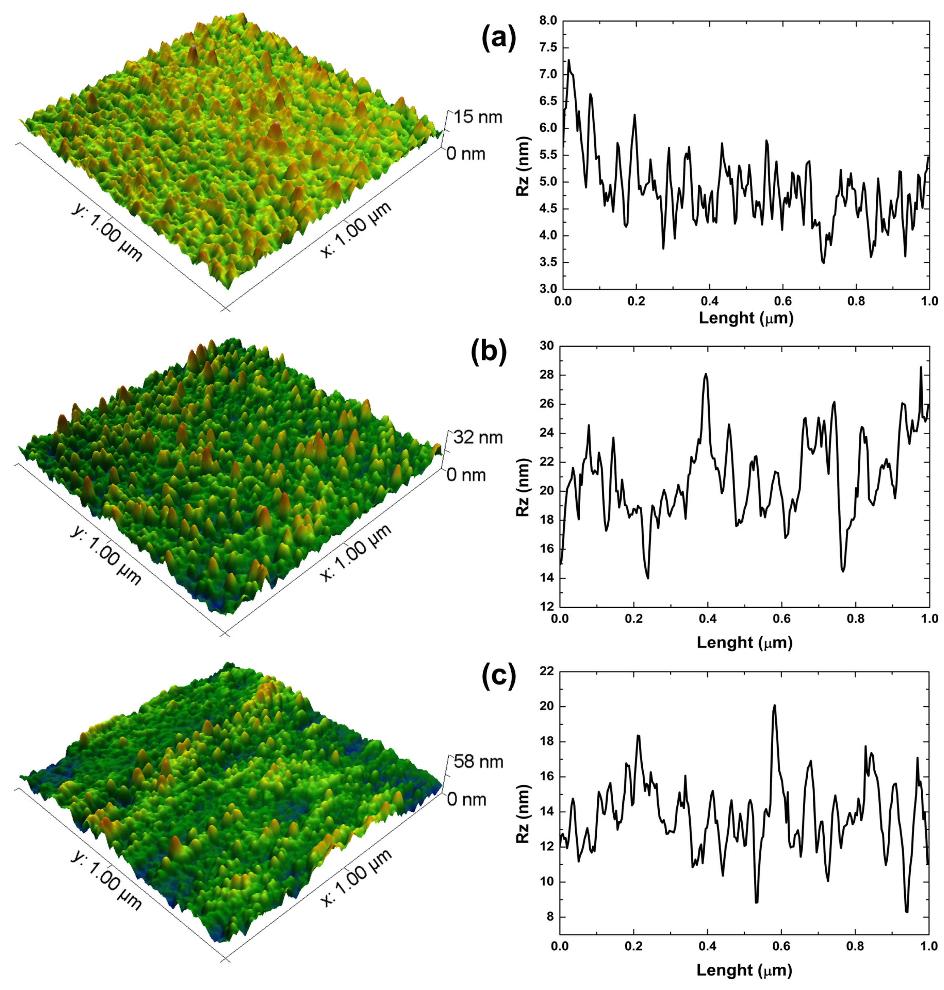
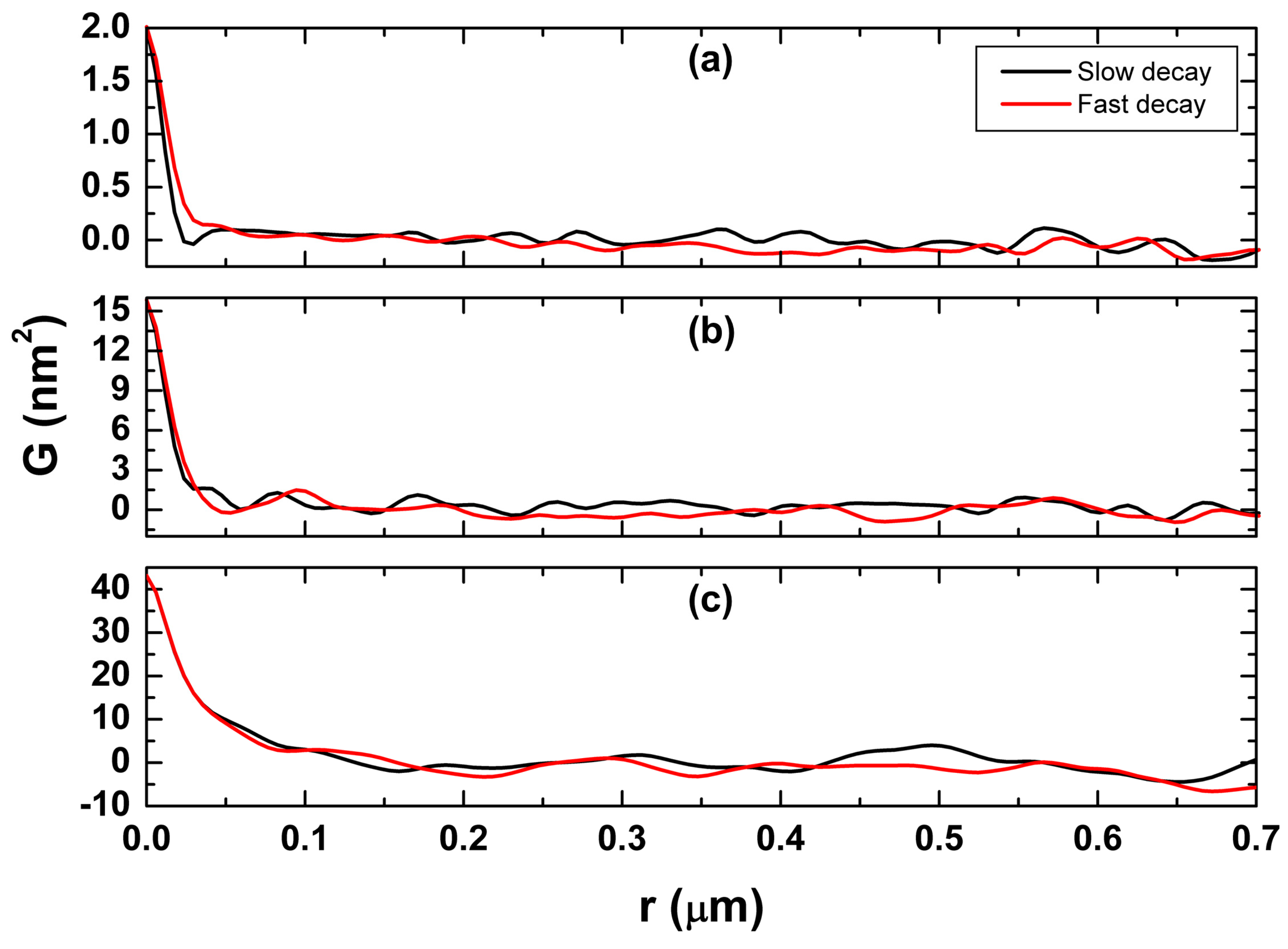
Areas of 1×1 μm2 were scanned by an atomic force microscope (Nanoscope Multimode Digital Instruments, Santa Barbara, CA, USA) with a scanning velocity of 1 Hz and silicon tips. All measurements were performed with no contact, in the air, and at four different regions on each sample, generating images with 256 pixels × 256 pixels at room temperature. To create the images, we used RTESPA-300 model tips (Bruker, San Jose, CA, USA), with a spring constant of 40 N/m and a tip radius of 8 nm. Our morphological parameters were obtained using Gwyddion 2.59 software [31] in accordance with ISO 25178-2: 2012 [32]. In addition to data referring to the autocorrelation function (ACF), fractal and multifractal analysis were also performed. We also computed the fractal succolarity (FS) through an algorithm developed in R and FORTRAN 77 [33]. To discuss the morphological spatial structures, Minkowski functionals (MFs), which are the volume (V), boundary (S), and connectivity ( χ ), were calculated according to Equations (1)–(3):
V = N w h i t e N ,
S = N b o u n d N ,
χ = C w h i t e C b l a c k N ,
In these equations, Nwhite represents the number of “white” pixels, N is the total number of pixels, Nbound is the number of white-black pixel boundaries, and Cwhite and Cblack are the numbers of continuous sets of white and black pixels, respectively. Furthermore, for proper analysis of the multifractal parameters, the AFM images were stored in a tiff file format characterized by a simple box counting. In this way, the generalized fractal dimensions were expressed as in Equation (4), and the multifractal spectrum function was expressed as in Equation (5) [34]:
  D q = τ ( q ) ( q 1 ) ,
f ( α ( q ) ) = q α ( q ) τ ( q ) ,
where α(q) = (q)/dq and the power exponent q ( ; + ) .

3. Results

The morphology of RF-PECVD sputtered individual Cu and Cu/Ni thin films, as well as their and Rz profiles, are shown in Figure 1. The Cu#0 sample showed the smoothest morphology with a uniform distribution of sharp, rough peaks, which was confirmed by its Rz pattern (Figure 1a). A similar morphology can be observed for the Cu/Ni#15 sample (Figure 1b), but its Rz pattern showed that there was a predominance of rough peaks and a detriment of valleys. However, the Cu/Ni#10 sample (Figure 1c) displayed a morphology that was entirely irregular and non-uniform, with a robust formation of rough islands. The Ni film deposited within 15 min had a significantly greater root mean square deviation roughness (Sq = 4.0 ± 0.4 nm) than the individual Cu film (Sq = 1.4 ± 0.2 nm), which further increased after 20 min of deposition (6.6 ± 0.7 nm). This proves that the Ni layer deposition time is critical for forming surfaces with different morphologies and surface roughness values. Such morphologies and roughness values are similar to the others previously reported [35,36], confirming that our RF-PECVD experiment is suitable for obtaining reproducible Cu/Ni thin films.
To further analyze the spatial profiles of the samples, we used an important physical parameter often used in film analysis: the ACF, which provides information about the degree of isotropy or anisotropy of the surface microtexture [37]. Thus, we used this parameter (together with the roughness parameter) to evaluate how the sputtering time affected the spatial distribution and organization of rough peaks on the surface of the Cu/Ni thin films. Herein, the autocorrelation functions were calculated using the AFM topographical maps using Gwyddion 2.59 software [31]. Figure 2 shows a set of ACFs calculated for these systems, obtained according to the lateral dimension of each AFM image. The red and black lines are associated with the fastest decay direction (τa1) and the slowest decay direction (τa2), respectively, which are angles responsible for dictating the direction and whose autocorrelation function drops down the threshold for their shortest and longest r values [38].
From the values summarized in Table 1, we computed that the τa1 values increased from Cu#0 to Cu/Ni#20, but the τa2 values robustly decreased. Such behavior was behind the increase in the lateral autocorrelation lengths Sa1 and Sa2 of Cu/Ni#15 and Cu/Ni#20, respectively, indicating that higher sputtering times provide more open surfaces [39], which can be ascribed to their different rougher profile. This is in complete agreement with our height-based analysis, because the surface roughness value increased from Cu/Ni#15 to Cu/Ni#20. Furthermore, the anisotropy ratio (Str), which dictates directional inhomogeneities of the surface microtexture, showed that all surfaces were strongly dominated by isotropic patterns (Str > 0.3) [40]. It is worth noting that the 3D spatial patterns of Cu/Ni#15 showed the highest degree of surface isotropy (Str = ~0.7), suggesting that its surface microtexture was composed of spatial patterns with significant directional inhomogeneities.
An advanced morphological analysis was performed using Minkowski functionals (MFs). In Figure 3, we see MFs are measures used to describe the geometric characteristics of nanosurfaces. The panels displayed in Figure 3a–c show the MFs computed considering the non-normalized threshold z. In this regard, we can see that it was not possible to make a fair comparison between the samples in the present case. Thus, we also computed the MFs considering the normalized threshold z, as shown in Figure 3d–f. Figure 3d reveals that the Minkowski volume for the Cu/Ni#15 and Cu/Ni#20 samples had a similar pattern when the normalized threshold was considered. This means that the distribution of matter as a function of height was similar in both cases. In Figure 3e,f, let z p be the normalized threshold associated with the corresponding Minkowski boundary and connectivity peak. We observed that z p was high for the Cu#0 sample, whereas the samples of Cu/Ni#15 and Cu/Ni#20 had close values of z p , which can be attributed to their high roughness values. This suggests that their percolative features were similar to each other but different from the percolative properties of the Cu#0 sample.
The advanced fractal parameters were used to study the surface microtexture’s irregularities [19]. The panels displayed in Figure 4 bring four fractal parameters as a function of the sample type. As can be seen, the fractal dimension (FD), Hurst coefficient (H), and topographical entropy (E) parameters showed no statistically significant difference (one-way ANOVA, p > 0.05). The FD values were found to be 2.44 ± 0.12 (Cu#0), 2.44 ± 0.12 (Cu/Ni#15), and 2.37 ± 0.12 (Cu/Ni#20), suggesting that all the films had similar spatial complexities. Due to the direct correlation with the FD value, the H values were computed to be 0.56 ± 0.03 (Cu#0), 0.56 ± 0.03 (Cu/Ni#15), and 0.63 ± 0.04 (Cu/Ni#20), showing that their surface microtextures were dominated by high dominant spatial frequencies [23]. Furthermore, all films displayed high topographical uniformity (E ~ 1) [22,23], specifically 0.98 ± 0.05 (Cu#0), 0.96 ± 0.05 (Cu/Ni#15), and 0.98 ± 0.05 (Cu/Ni#20), suggesting that their surface microtextures were composed of 3D spatial patterns evenly arranged over the surface. Such topographical uniformity can be attributed to the surface isotropy exhibited by all surfaces (Str > 0.3). Nonetheless, the fractal succolarity (FS) of Cu#0 was determined to be 0.57 ± 0.01, while Cu/Ni#15 (0.53 ± 0.02) and Cu/Ni#20 (0.53 ± 0.02) yielded similar values which were close to the ideal value (0.5) [19]. The one-way ANOVA comparison test confirmed that the overall average values were statistically different (p < 0.5). However, the pairwise ANOVA-based Tukey test indicated that the Cu/Ni#15 and Cu/Ni#20 samples showed no statistically significant difference. This proves that the Cu/Ni films have similar surface percolation, which perfectly agrees with our Minkowski functional morphological analysis (Figure 3).
The vertical growth dynamics associated with local irregularities of the surface of the films were investigated using their multifractal spectra [38]. Figure 5 reveals three clear fingerprints of multifractality on the surface of the investigated thin films. Panel (a) shows a deviation from the linear behavior between the mass exponent τ(q) and q. Panel (b) indicates a non-constant relationship between the generalized dimensions Dq and q. Panel (c) presents the usual downward concave curve of the multifractal spectra. Moreover, Table 2 shows the measures that quantify the multifractality of the thin films explicitly [28].
The spectra width Δα = αmax • αmin is the most important multifractal measure that represents the strength of the multifractal nature assumed by a surface. In this regard, we see that the value of Δα for Cu/Ni#20 was higher than the corresponding value for Cu/Ni#15, which in turn was higher than the value for the Cu#0 sample. Such results suggest that the sputtering time plays an important role in designing Cu/Ni thin films with high multifractality and different vertical growth dynamics.
In order to quantify the scaling symmetry and asymmetry, we employed a newly developed approach [41]. First, note that in the parabolic-like curve of Figure 5c, the left (right) branch accounts for the scaling behavior of the regions of the peaks (valleys). Thus, from a symmetry-based approach, Δf = f(αmax) − f(αmin) can be employed as a quantifier of the deviation of the analyzed topography from the perfect monofractal behavior; that is, Δf provides information about the scaling symmetry of the surfaces. In Table 2, the values of Δf show that the samples of Cu#0 presented the largest deviation from perfect monofractality in comparison with the {Cu/Ni#15, Cu/Ni#20} signaling and that the sputtering process induced a decrease in the scaling symmetry in these topographies, even though it produced an increase in their multifractality, as was previously noted; that is, the scaling behavior of the top and bottom segments of the {Cu/Ni#15, Cu/Ni#20} topographies was more symmetric than the corresponding one of the pure Cu#0. This analysis points out that the vertical growth dynamics of the individual Cu and Cu/Ni thin films differed regarding multifractality and scaling symmetry.

4. Conclusions

We investigated the morphological, fractal, and multifractal properties of bimetallic Cu/Ni thin films deposited onto SiO2 substrates using an RF-PECVD apparatus. Using 3D AFM topographic maps, we investigated their morphologies and roughness in addition to the Minkowski functionals, advanced fractal parameters, and multifractal features. The films displayed different morphologies and roughness profiles, dictated by their singular directional inhomogeneities. The Minkowski volume showed that the Cu/Ni films deposited after 15 and 20 min had a similar relative distribution of matter as a function of height, which was different from the individual Cu films. Accordingly, the Minkowski boundary and Minkowski connectivity pointed out that the Cu/Ni samples’ percolative properties were similar but distinct from the Cu sample’s percolative features. The surface microtexture of the films showed similar spatial complexity, dominant spatial frequencies, and topographical uniformity. However, their surface percolation was dictated by the type of film analyzed, where the Cu/Ni thin films exhibited similar surface percolation properties, confirming the Minkowski functional morphological analysis. We also observed clear fingerprints of multifractal behavior in all the samples. The results indicate that the sputtering process favored the formation of topographies with an enhanced multifractality degree but with a weakened scaling asymmetry. Our findings suggest that sputtering can tune the films’ percolative properties, multifractality, and scaling symmetry, inducing different vertical growth dynamics. Such behavior can help improve the fabrication of bimetallic thin films with morphology and roughness controlled. This can dictate new perspectives for producing devices coated with Cu/Ni layers (e.g., functionalized AFM tips with remarkable molecular recognition imaging) for unequivocally distinguishing hybrid molecular surfaces.

Author Contributions

Conceptualization, methodology, resources, validation, visualization, and writing—review and editing, R.S.M. and N.S.F.; data curation, formal analysis, investigation, and writing—original draft preparation, Ş.Ţ., A.G. and S.S.; writing—original draft preparation, writing—review, and project administration, M.A.P., E.A.S. and H.D.d.F.F. All authors have read and agreed to the published version of the manuscript.

Funding

This research received no external funding.

Institutional Review Board Statement

Not applicable.

Informed Consent Statement

Not applicable.

Data Availability Statement

The data that support the findings of this study are available from the corresponding author upon reasonable request.

Conflicts of Interest

The authors declare no conflict of interest.

References

  1. Hassan, K.; Iftekhar Uddin, A.S.; Chung, G.-S. Fast-response hydrogen sensors based on discrete Pt/Pd bimetallic ultra-thin films. Sens. Actuators B Chem. 2016, 234, 435–445. [Google Scholar] [CrossRef]
  2. Ma, M.; Hansen, H.A.; Valenti, M.; Wang, Z.; Cao, A.; Dong, M.; Smith, W.A. Electrochemical reduction of CO2 on compositionally variant Au-Pt bimetallic thin films. Nano Energy 2017, 42, 51–57. [Google Scholar] [CrossRef] [Green Version]
  3. Gaković, B.; Danilov, P.A.; Kudryashov, S.I.; Milovanović, D.; Radulović, A.; Panjan, P.; Ionin, A.A. The morphological and compositional changes of bimetallic Ti/Al thin film induced by ultra-short laser pulses. Eur. Phys. J. D 2021, 75, 288. [Google Scholar] [CrossRef]
  4. Qiu, C.; Shang, R.; Xie, Y.; Bu, Y.; Li, C.; Ma, H. Electrocatalytic activity of bimetallic Pd–Ni thin films towards the oxidation of methanol and ethanol. Mater. Chem. Phys. 2010, 120, 323–330. [Google Scholar] [CrossRef]
  5. Pötzelberger, I.; Mardare, A.I.; Hassel, A.W. Electrocatalytic oxidation of glucose by screening combinatorial copper-nickel alloys. Phys. Status Solidi 2016, 213, 1434–1440. [Google Scholar] [CrossRef]
  6. Pötzelberger, I.; Mardare, A.I.; Hassel, A.W. Non-enzymatic glucose sensing on copper-nickel thin film alloy. Appl. Surf. Sci. 2017, 417, 48–53. [Google Scholar] [CrossRef]
  7. Khadom, A.A.; Yaro, A.S. Modeling of corrosion inhibition of copper-nickel alloy in hydrochloric acid by benzotriazole. Russ. J. Phys. Chem. A 2011, 85, 2005–2012. [Google Scholar] [CrossRef]
  8. Vishwakarma, V.; Josephine, J.; George, R.P.; Krishnan, R.; Dash, S.; Kamruddin, M.; Kalavathi, S.; Manoharan, N.; Tyagi, A.K.; Dayal, R.K. Antibacterial copper–nickel bilayers and multilayer coatings by pulsed laser deposition on titanium. Biofouling 2009, 25, 705–710. [Google Scholar] [CrossRef] [PubMed]
  9. Wang, Y.; Zhang, R.; Duan, J.; Shi, X.; Zhang, Y.; Guan, F.; Sand, W.; Hou, B. Extracellular Polymeric Substances and Biocorrosion/Biofouling: Recent Advances and Future Perspectives. Int. J. Mol. Sci. 2022, 23, 5566. [Google Scholar] [CrossRef]
  10. Pandis, N.; Polychronopoulou, A.; Eliades, T. Alleviation of mandibular anterior crowding with copper-nickel-titanium vs nickel-titanium wires: A double-blind randomized control trial. Am. J. Orthod. Dentofac. Orthop. 2009, 136, e1–e152. [Google Scholar] [CrossRef]
  11. Mönig, H. Copper-oxide tip functionalization for submolecular atomic force microscopy. Chem. Commun. 2018, 54, 9874–9888. [Google Scholar] [CrossRef] [PubMed]
  12. Marcuello, C.; de Miguel, R.; Lostao, A. Molecular Recognition of Proteins through Quantitative Force Maps at Single Molecule Level. Biomolecules 2022, 12, 594. [Google Scholar] [CrossRef] [PubMed]
  13. Gheorghiu, C.C.; Ionescu, A.; Zai, M.-I.; Iancu, D.; Burducea, I.; Velisa, G.; Vasile, B.S.; Ianculescu, A.C.; Bobeica, M.; Popa, D.; et al. Nanoscale Control of Structure and Composition for Nanocrystalline Fe Thin Films Grown by Oblique Angle RF Sputtering. Materials 2022, 15, 6134. [Google Scholar] [CrossRef] [PubMed]
  14. Limwichean, S.; Kasayapanand, N.; Ponchio, C.; Nakajima, H.; Patthanasettakul, V.; Eiamchai, P.; Meng, G.; Horprathum, M. Morphology-controlled fabrication of nanostructured WO3 thin films by magnetron sputtering with glancing angle deposition for enhanced efficiency photo-electrochemical water splitting. Ceram. Int. 2021, 47, 34455–34462. [Google Scholar] [CrossRef]
  15. Barbee, B.; Muchharla, B.; Adedeji, A.; Karoui, A.; Kumar Sadasivuni, K.; Sha, M.S.; Abdullah, A.M.; Slaughter, G.; Kumar, B. Cu and Ni Co-sputtered heteroatomic thin film for enhanced nonenzymatic glucose detection. Sci. Rep. 2022, 12, 7507. [Google Scholar] [CrossRef]
  16. Nikpasand, K.; Elahi, S.M.; SarI, A.H.; Boochani, A. Surface micromorphology analysis of Cu/Ni nanocomposite thin films by power spectra density and fractal geometry. Mater. Sci. 2020, 38, 328–333. [Google Scholar] [CrossRef]
  17. Das, A.; Matos, R.S.; Pinto, E.P.; Yadav, R.P.; Ţălu, Ş.; Kumar, S. 3D micromorphology-contact resistance-conductivity insights of quasi 2D Cd1-xPbxS thin films: Investigation based on stereometric and fractal analysis. Mater. Chem. Phys. 2022, 278, 125635. [Google Scholar] [CrossRef]
  18. Zhang, F.; Edwards, D.; Deng, X.; Wang, Y.; Kilpatrick, J.I.; Bassiri-Gharb, N.; Kumar, A.; Chen, D.; Gao, X.; Rodriguez, B.J. Investigation of AFM-based machining of ferroelectric thin films at the nanoscale. J. Appl. Phys. 2020, 127, 034103. [Google Scholar] [CrossRef]
  19. Ţălu, Ş.; Abdolghaderi, S.; Pinto, E.P.; Matos, R.S.; Salerno, M. Advanced fractal analysis of nanoscale topography of Ag/DLC composite synthesized by RF-PECVD. Surf. Eng. 2020, 36, 713–719. [Google Scholar] [CrossRef]
  20. Das, A.; Chawla, V.; Matos, R.S.; da Fonseca Filho, H.D.; Yadav, R.P.; Ţălu, Ş.; Kumar, S. Surface microtexture and wettability analysis of quasi two-dimensional (Ti, Al)N thin films using fractal geometry. Surf. Coatings Technol. 2021, 421, 127420. [Google Scholar] [CrossRef]
  21. Das, A.; Yadav, R.P.; Chawla, V.; Kumar, S.; Ţălu, Ş.; Pinto, E.P.; Matos, R.S. Analyzing the surface dynamics of titanium thin films using fractal and multifractal geometry. Mater. Today Commun. 2021, 27, 102385. [Google Scholar] [CrossRef]
  22. Romaguera-Barcelay, Y.; Pedraça, A.S.; Moreira, J.A.; Almeida, A.; Tavares, P.B.; Brito, W.R.; Matos, R.S.; Pires, M.A.; Pinto, E.P.; da Fonseca Filho, H.D. Evaluation of nanostructured BiZn0.5Ti0.5O3 thin films deposited by RF magnetron sputtering. Mater. Sci. Eng. B 2021, 267, 115090. [Google Scholar] [CrossRef]
  23. Ţălu, Ş.; Matos, R.S.; Pinto, E.P.; Rezaee, S.; Mardani, M. Stereometric and fractal analysis of sputtered Ag-Cu thin films. Surf. Interfaces 2020, 21, 100650. [Google Scholar] [CrossRef]
  24. Zhou, W.; Cao, Y.; Zhao, H.; Li, Z.; Feng, P.; Feng, F. Fractal Analysis on Surface Topography of Thin Films: A Review. Fractal Fract. 2022, 6, 135. [Google Scholar] [CrossRef]
  25. Jing, C.; Tang, W. Ga-doped ZnO thin film surface characterization by wavelet and fractal analysis. Appl. Surf. Sci. 2016, 364, 843–849. [Google Scholar] [CrossRef]
  26. Astinchap, B. Fractal and statistical characterization of Ti thin films deposited by RF-magnetron sputtering: The effects of deposition time. Optik 2019, 178, 231–242. [Google Scholar] [CrossRef]
  27. Hosseinpanahi, F.; Raoufi, D.; Ranjbarghanei, K.; Karimi, B.; Babaei, R.; Hasani, E. Fractal features of CdTe thin films grown by RF magnetron sputtering. Appl. Surf. Sci. 2015, 357, 1843–1848. [Google Scholar] [CrossRef]
  28. Ghosh, K.; Pandey, R.K. Annealing time induced roughening in ZnO thin films: A fractal and multifractal assessment. Mater. Sci. Semicond. Process. 2020, 106, 104771. [Google Scholar] [CrossRef]
  29. Ghosh, K.; Pandey, R.K. Fractal and multifractal analysis of In-doped ZnO thin films deposited on glass, ITO, and silicon substrates. Appl. Phys. A 2019, 125, 98. [Google Scholar] [CrossRef]
  30. Ghaderi, A.; Shafiekhani, A.; Solaymani, S.; Ţălu, Ş.; da Fonseca Filho, H.D.; Ferreira, N.S.; Matos, R.S.; Zahrabi, H.; Dejam, L. Advanced microstructure, morphology and CO gas sensor properties of Cu/Ni bilayers at nanoscale. Sci. Rep. 2022, 12, 12002. [Google Scholar] [CrossRef]
  31. Nečas, D.; Klapetek, P. Gwyddion: An open-source software for SPM data analysis. Cent. Eur. J. Phys. 2012, 10, 181–188. [Google Scholar] [CrossRef]
  32. Blateyron, F. Characterisation of Areal Surface Texture; Leach, R., Ed.; Springer: Berlin/Heidelberg, Germany, 2013; ISBN 978-3-642-36457-0. [Google Scholar]
  33. de Melo, R.H.C.; Conci, A. Succolarity: Defining a Method to Calculate This Fractal Measure. In Proceedings of the 15th International Conference on Systems, Signals and Image Processing, Bratislava, Slovakia, 25–28 June 2008; pp. 291–294. [Google Scholar] [CrossRef]
  34. Ţălu, Ş. Micro and nanoscale Characterization of three Dimensional Surfaces; Napoca Star Publishing House: Cluj-Napoca, Romania, 2015. [Google Scholar]
  35. Ghodselahi, T.; Arman, A. Magnetoresistance of Cu–Ni nanoparticles in hydrogenated amorphous carbon thin films. J. Mater. Sci. Mater. Electron. 2015, 26, 4193–4197. [Google Scholar] [CrossRef]
  36. Arman, A.; Ghodselahi, T.; Molamohammadi, M.; Solaymani, S.; Zahrabi, H.; Ahmadpourian, A. Microstructure and optical properties of Cu@Ni nanoparticles embedded in a-C:H. Prot. Met. Phys. Chem. Surfaces 2015, 51, 575–578. [Google Scholar] [CrossRef]
  37. Matos, R.S.; da Costa, Í.C.; Yasumura, H.D.; de Azevedo, S.G.; Sanches, E.A.; da Fonseca Filho, H.D. Nanoscale surface dynamics of spatial patterns of polymeric bilayered particles loaded with essential oil. Microsc. Res. Tech. 2022, 85, 3633–3641. [Google Scholar] [CrossRef] [PubMed]
  38. Ramos, G.Q.; Matos, R.S.; Das, A.; Kumar, S.; Ţălu, Ş.; da Fonseca Filho, H.D. Correlating Morphology and Multifractal Spatial Patterns of the Leaf Surface Architecture of Anacardium occidentale L. Fractal Fract. 2022, 6, 320. [Google Scholar] [CrossRef]
  39. Davim, J.P. Tribology for Engineers: A Practical Guide; Woodhead Publishing Limited: Cambridge, UK, 2011; p. 296. [Google Scholar]
  40. Blateyron, F. The Areal Field Parameters. In Characterisation of Areal Surface Texture; Springe: Berlin/Heidelberg, Germany, 2013; pp. 15–43. ISBN 9783642364587. [Google Scholar]
  41. Constantoudis, V.; Ioannou-Sougleridis, I.; Dimou, A.; Ninou, A.; Chatzichristidi, M.; Makarona, E. A symmetry-based approach to the characterization of complex surface morphologies: Application in CuO and NiO nanostructures. Micro Nano Eng. 2022, 16, 100148. [Google Scholar] [CrossRef]
Figure 1. Representative 3D AFM topographical maps and Rz profiles of (a) Cu#0, (b) Cu/Ni#15, and (c) Cu/Ni#20 thin films.
Symmetry 14 02675 g001
Figure 2. The autocorrelation functions (ACFs) as a function of the sample length (r) of (a) Cu#0, (b) Cu/Ni#15, and (c) Cu/Ni#20 thin films.
Symmetry 14 02675 g002
Figure 3. (ac) MFs considering the non-normalized threshold z and (df) MFs considering the normalized threshold z for the scanning area of 1 μm × 1 μm.
Symmetry 14 02675 g003
Figure 4. (a) Fractal dimension, (b) topographical entropy, (c) fractal succolarity, and (d) Hurst coefficient of individual Cu and Cu/Ni thin films as a function of the sample type.
Symmetry 14 02675 g004
Figure 5. (a) Mass exponent τ(q), (b) generalized dimensions Dq, and (c) multifractal spectra (f(α) versus α of individual Cu and Cu/Ni thin films as a function of the order of moments. For clarity, the mass exponent curves for Cu/Ni#15 and Cu/Ni#20 have been shifted by +5 and +10, respectively.
Symmetry 14 02675 g005
Table 1. The fastest (τa1) and the slowest (τa2) decay directions, decay lengths (Sa1 and Sa2), and anisotropy factors (Str) for the investigated representative samples.
ParameterUnitCu#0Cu/Ni#15Cu/Ni#20
τa1º13.8171.5787.27
ta2º30.8812.994.840
Sa1nm8.13318.5341.06
Sa2nm71.5726.06115.6
Str-0.4470.7110.355
Table 2. Multifractal parameters of individual Cu and Cu/Ni thin films.
ParameterCu#0Cu/Ni#15Cu/Ni#20
f(αmax)−0.353−0.204−0.261
f(αmin)1.5601.2711.289
Δf1.9131.4751.550
αmax2.9792.9193.040
αmin2.0471.9631.978
Δα0.9320.9561.062
Publisher’s Note: MDPI stays neutral with regard to jurisdictional claims in published maps and institutional affiliations.

