Article

Flexoelectric and Piezoelectric Coupling in a Bended MoS2 Monolayer

by
Hanna V. Shevliakova
1,2,
Semen O. Yesylevskyy
1,
Ihor Kupchak
3,
Galina I. Dovbeshko
1,
Yunseok Kim
4 and
Anna N. Morozovska
1,*
1
Institute of Physics, National Academy of Sciences of Ukraine, pr. Nauky 46, 03028 Kyiv, Ukraine
2
Department of Microelectronics, Igor Sikorsky Kyiv Polytechnic Institute, 03056 Kyiv, Ukraine
3
Institute of Semiconductor Physics of NAS of Ukraine, 03028 Kyiv, Ukraine
4
School of Advanced Materials Science and Engineering, Sungkyunkwan University (SKKU), Suwon 16419, Korea
*
Author to whom correspondence should be addressed.
Symmetry 2021, 13(11), 2086; https://doi.org/10.3390/sym13112086
Submission received: 29 September 2021 / Revised: 24 October 2021 / Accepted: 28 October 2021 / Published: 3 November 2021

Abstract

:
Low-dimensional (LD) transition metal dichalcogenides (TMDs) in the form of nanoflakes, which consist of one or several layers, are the subject of intensive fundamental and applied research. The tuning of the electronic properties of the LD-TMDs are commonly related with applied strains and strain gradients, which can strongly affect their polar properties via piezoelectric and flexoelectric couplings. Using the density functional theory and phenomenological Landau approach, we studied the bended 2H-MoS2 monolayer and analyzed its flexoelectric and piezoelectric properties. The dependences of the dipole moment, strain, and strain gradient on the coordinate along the layer were calculated. From these dependences, the components of the flexoelectric and piezoelectric tensors have been determined and analyzed. Our results revealed that the contribution of the flexoelectric effect dominates over the piezoelectric effect in both in-plane and out-of-plane directions of the monolayer. In accordance with our calculations, a realistic strain gradient of about 1 nm−1 can induce an order of magnitude higher than the flexoelectric response in comparison with the piezoelectric reaction. The value of the dilatational flexoelectric coefficient is almost two times smaller than the shear component. It appeared that the components of effective flexoelectric and piezoelectric couplings can be described by parabolic dependences of the corrugation. Obtained results are useful for applications of LD-TMDs in strain engineering and flexible electronics.

1. Introduction

Layered transition metal dichalcogenides (TMDs) in the form of bulk materials are typically non-polar centrosymmetric semiconductors with a relatively wide band gap (~1.1–2 eV) and specific shape of the Fermi surface [1,2]. On transition from the bulk to the nanoscale, additional long-range orderings and physical properties, such as piezoelectric, or ferroelectric [3,4,5], semiconductive, semi-metallic or metallic [6,7,8] were found in different structural phases (polymorphs) of TMD monolayers [9]. In particular, the polar and semiconducting properties of the low-dimensional (LD) TMDs with a chemical formula MX2 (M—metal Mo, V, W; X—chalcogen S, Se, Te) [10,11] and Janus-compounds with a chemical formula MXY (X, Y—chalcogens) [12,13] vary from non-polar to ferroelectric state, and from direct-band semiconductor to metallic conductivity.
The strain and strain gradient impact on LD-TMD polar and electronic properties can be principally important for the properties control, and therefore LD semiconductor materials, such as graphene, MX2 and MXY monolayers, are ideal candidates for the strain engineering [14] and recently introduced “straintronics” [15]. Their strain-induced conductive domain walls can act as mobile charged channels, similarly to the “domain wall nanoelectronics” in multiferroic thin films [16,17,18] and graphene-on-ferroelectric nanostructures [19,20]. There are remarkable possibilities for tuning the structural, polar and electronic properties of LD-TMDs by application of either homogeneous elastic strains [21,22] or inhomogeneous curvature-induced strain gradients [23,24]. In particular, Duerloo et al. [6] predicted a strain-induced phase transition from a semiconducting 2H to a metallic 1T’ phase in various MX2. Subsequently, Song et al. [25] observed a room temperature semiconductor−metal transition in thin MoTe2 films induced by a homogeneous tensile strain of 0.2%.
A number of first-principle studies explored surface-induced piezoelectricity [26,27] and ferroelectric polarization [5,28] in various MX2 and MXY. Subsequently, the possible mechanism of the ferroelectric state appearance in LD-TMDs was described by the Landau–Ginzburg–Devonshire (LGD) continuous approach [29]. Since only in-plane ferroelectricity can exist in a geometrically flat pure centrosymmetric MX2 layer, LGD analysis suggests that the switchable out-of-plane ferroelectric polarization emerges due to the rare-earth doping and predicts that the domain walls in LD-TDMs should become conductive above a certain strain threshold.
The physical origin of the bending-induced changes of LD-TMDs electronic and polar properties can be similar to the ones in a bended graphene [30,31] and boron nitride [32]; moreover, the flexoelectric effect plays an important role [33,34]. It was predicted theoretically that the bending can induce an out-of-plane electric dipole moment of carbon nanoshells [35]. As anticipated, the bending-induced dipole moment is curvature-dependent, and strong curvatures can lead to a relatively high polarization of LD-TMDs, induced by a flexoelectric effect [36,37]. The bending-induced out-of-plane dipole moment with density p ~ ( 0.01 0.4 ) C/nm and flexoelectric polarization P ~ ( 0.1 2 ) μ C/cm2 were calculated from the first principles for MoS2 [5], WS2 [35], and WTe2 [38,39] single-layers. The flexoelectricity is determined by the lattice deformation in dielectrics and wide gap ferroelectrics. In contrast to this, centrosymmetric narrow gap semiconductors and semimetals, such as MX2, contain a significant contribution from the deformed electronic density [32,40,41], and thus the electronic contribution to their flexoelectric response can dominate over the lattice-mediated ionic contribution, especially under photoexcitation [42,43].
The tunable out-of-plane piezoelectricity and enhanced conductivity, both induced by flexoelectricity, were observed by Kang et al. [23] in semiconducting 2H-MoTe2 flakes by creating surface corrugation. The experimental results were corroborated by their ab initio calculations [23], analytical calculations performed within LGD approach [44], and finite element modeling [45]. Specifically, the LGD approach explores the flexoelectric origin of the polarization induced by a spontaneous bending and by inversion symmetry breaking due to the interactions with substrate. Finite element modeling allows calculating the elastic and electric fields, flexoelectric polarization, and its correlation with free charge density for a TMD nanoflake placed on a rough substrate with a sinusoidal profile of the corrugation [45].
Despite the progress, the complete information about the piezoelectric and flexoelectric coupling tensors in LD-TMDs is lacking, and the influence of the tensor symmetry and numerical values of its components on polar and electronic phenomena in LD-TMDs has not been studied. Since the couplings are important for LD objects, their knowledge is required to control and predict the physical properties of LD-TMDs for their novel applications in nanoelectronics and advanced memories. Using the density functional theory (DFT) and phenomenological Landau approach, in this work, we consider the curved monolayer of 2H-MoS2 in order to calculate the nonzero components of its flexoelectric and piezoelectric coupling tensors and to analyze their possible dependence on the layer corrugation and surface-induced symmetry lowering.

2. Theoretical Formalism

The static electric polarization of a LD-TMD, P i ( x ) , has the form:
P i ( x ) f i j k l u k l x j + e i j k s t u j k ε 0 χ i j φ x j .
Here, f i j k l is the static flexoelectric tensor [46] determined by the microscopic properties of the material [47,48], u i j ( x ) is the elastic strain tensor, e i j k s is the tensor of the surface-induced piezoelectric effect [49,50], and t   is the thickness of a nanoflake. The last term in Equation (1) is proportional to the gradient of electric potential φ ( x ) , ε 0 is a universal dielectric constant, and χ i j is a real part of the TMD dielectric susceptibility. Einstein summation over repeated indexes is used hereinafter.

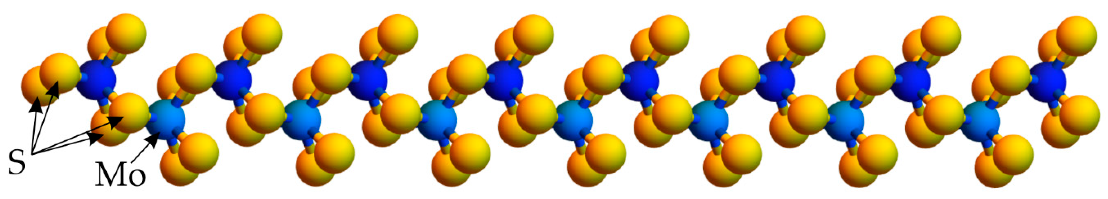
2.1. Ab Initio Calculations of the Flat and Corrugated MoS2 Nanolayer

We performed the calculations of the atomic position in the MoS2 nanolayer for the case of a flat layer and for 1–10% corrugated layers with a 1% step in corrugation within the DFT [51] in the generalized gradient approximation, implemented in the Quantum Espresso code [52]. We used ultrasoft Perdew-Burke-Ernzerhof pseudopotentials [53], which include 14 valence electrons for molybdenum and six valence electrons for sulfur. An integration of the Brillouin zone was performed using 1 × 14 × 1 k-points mesh centered on Γ in the Brillouin zone, generated by Monkhorst-Pack scheme [54], and Methfessel-Paxton smearing [55] with a parameter of 0.005 Ry. We applied 50 Ry cutoff for smooth part of the wave function and 350 Ry for the augmented charge density to ensure a sufficient convergence of the results.
The MoS2 monolayer was modeled by a supercell approach with 25 Å of vacuum layer added to avoid a coulomb interaction between the periodic images. Initial (flat) layer was built with experimental value of the lattice constant of 3.161 Å and contained 48 atoms (Figure 1). For the corrugated layers, we reduced the lattice constant of the supercell in x-direction and modulated the atomic z (out-of-plane) coordinates by suitable sinusoidal distribution to match an integer value of corrugation. After that, all the systems were relaxed through all the internal coordinates until the Hellmann-Feynman forces became less than 10−4 atomic units, and at this point, all the necessary quantities (atomic coordinates and wave functions) were extracted. The difference between the initial corrugation and that obtained for the corresponding relaxed system does not exceed few percentages of their values. Therefore, the calculations revealed that the bending in the z-direction is sinusoidal along the x-axis (Figure 2).
In addition to the position of the atoms, the Bader charges [56] were computed. The distribution of the charges appeared to be uniform in a flat system and equal to Q M o = 1.083 e for molybdenum atoms and is Q S = 0.5415   e for sulfur atoms, where e = 1.60217662   · 10 19 C is the elementary charge. For strongly curved layers with a bending of 8–10%, a harmonic dependence of the charges on the x coordinate was observed (as shown in Figure 3). However, the difference between the maximal and minimal charges appeared to be small (see the scale in Figure 3) and close to the magnitude of expected numerical error. The effect of such a distribution on the electrophysical parameters of the layer is neglected hereinafter. This means that we neglect the terms proportional to the deformation potential in Equation (1), as the first approximation, and extract the terms proportional to the net flexoelectric coefficient, f i j k l , from the DFT results. The charge variations can be found as the second approximation, which becomes important for large curvatures only [32].
To the best of our knowledge, Figure 3 calculated for MoS2 has only qualitative analogue in the literature. Namely, the redistribution of Bader charges caused by the bending of phosphorene [33] and graphene [34] nanoribbons was calculated, and it appeared that the symmetries of Bader charges are broken under the applied strain gradient. This symmetry breaking is almost absent for the studied MoS2 (compare Figure 3 in this work with Figure 2 from [33] and Figure 4 from [34]), but evidently present for the phosphorene and graphene nanoribbons. The possible reason is the small discrepancy in the net Bader charges of sulfur in a bended MoS2 monolayer, which are smaller than the charge discrepancy in phosphorene [33] and graphene [34].

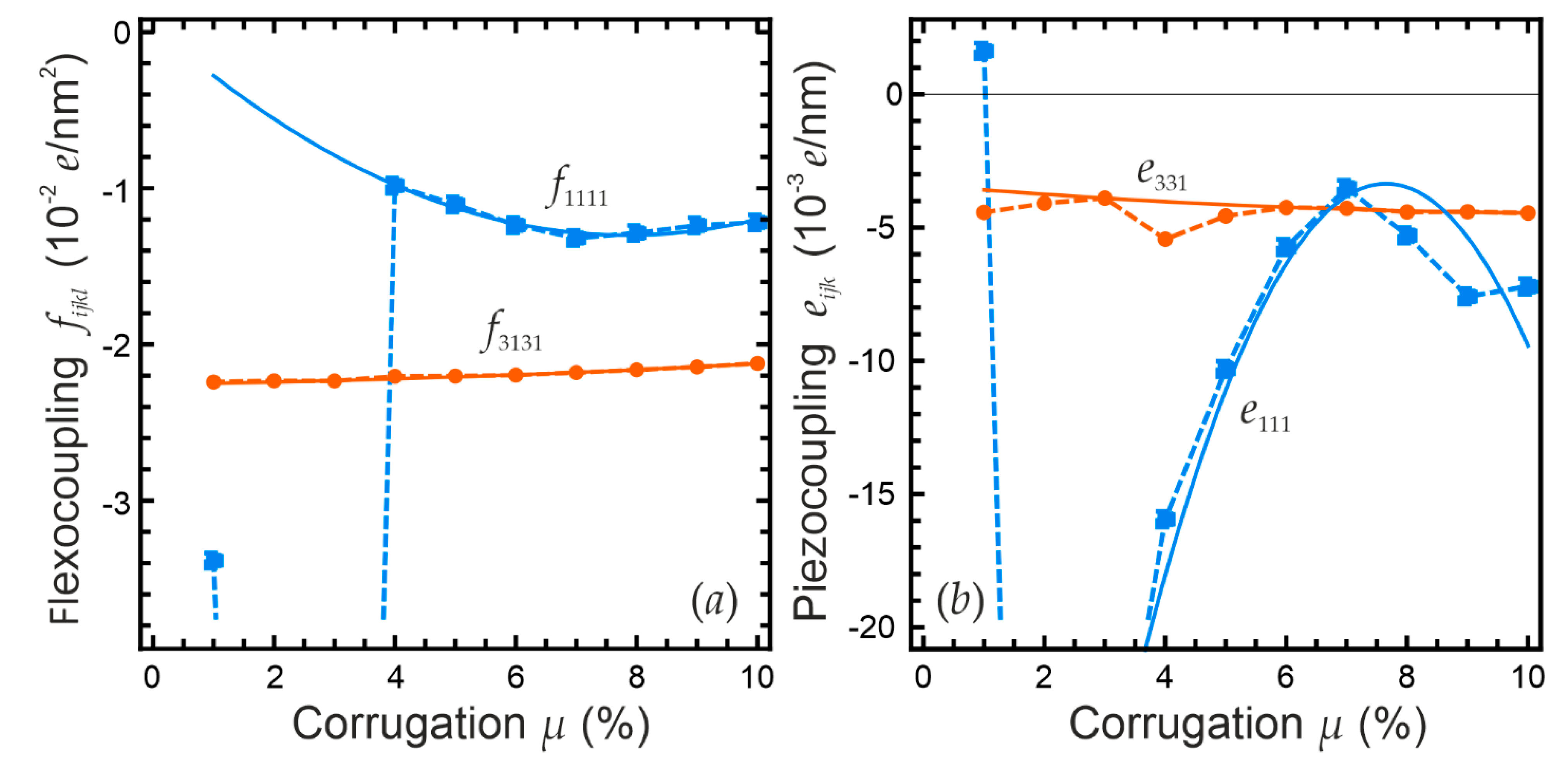
2.2. Determination of the Flexoelectric Coefficients from Ab Initio Calculations

The components of the piezoelectric and flexoelectric tensors for the 2H-MoS2 that belong to the point symmetry group 6/mmm can be determined from the equations:
d z ( x ) = e z z x u z x ( x ) + e z x x u x x ( x ) + f z x z x u z x , x ( x ) + f z x x x u x x , x ( x ) ,
d x ( x ) = e x z x u z x ( x ) + e x x x u x x ( x ) + f x x x z u x z , x ( x ) + f x x x x u x x , x ( x ) ,
where d i is projection of the elementary dipole moment on the axis i; u i j and u i j , k are strain tensor and strain gradient, respectively; e i j k and f i j k l are the components of the piezoelectric and flexoelectric tensors in Cartesian coordinates.
All nonzero components of d i , u i j and u i j , k were calculated in Mathematica 12.2 ®Wolfram Research notebook [57] based on the DFT results. In particular, the effective elementary dipole moment d of each dipole (see Figure 4) was calculated from the following equation:
d i = r Mo i | Q Mo | k = 1 6 r S i k | Q S 3 | ,
where r Mo i = { x Mo , y Mo , z Mo } i and r S i k = { x S , y S , z S } i k is a radius vector of the Mo and S atoms, respectively.
Further dependences were plotted on the x coordinate of the mass center of the dipole, and its radius vector was determined by the equation:
r ( j , i ) = 1 m Mo + 6   m S ( r Mo ( j , i ) m Mo +   k = 1 6 r S k ( j , i ) m S ) ,
where “ j ” is the percentage of corrugation, “ i ” is the dipole number, m M o = 95.9 g mol and m S = 32   g mol are atomic masses of molybdenum and sulfur, respectively. The points in Figure 5b and Figure 6b show the dependence of x-axis and y-axis projection of the dipole moment on x-coordinate of the dipole mass center.
Using the radius vector, the elementary displacement of the mass centers is calculated from the equation:
U ( j , i ) = r ( 0 , i ) r ( j , i ) ,
where r ( 0 , i ) is the radius vector of i-th dipole of the undeformed layer, r ( j , i ) is the radius vector of i-th dipole of the layer with corrugation j%. The dependences of the x-axis and y-axis projections of the displacement vector U ( j ) on x coordinate of the mass center (5) are shown in Figure 5a and Figure 6a, respectively.
Solid curves in Figure 5a,b and Figure 6a,b are harmonic (sinusoidal and co-sinusoidal) functions, which were selected in the form:
d z = d z c cos ( k x ) + d z s sin ( k x ) ,
d x = d x s   sin ( 2 k x ) + d x c   cos ( 2 k x ) + c .
Here, the coefficients d z c , d z s , d x s , d x c and c are fitting parameters. Theirs numerical values are selected to reach the best fit of the points in Figure 5b and Figure 6b.
The dependence of the displacement projections on x-axis was approximated by the functions:
U z ( x ) U 0 cos ( k x ) ,
U x ( x ) V 0 x + W 0 cos ( 2 k x ) .
Here, the coefficients U 0 , V 0 , and W 0 are fitting parameters. Theirs numerical values are selected to reach the best fit of the points in Figure 5a and Figure 6a.
The displacement causes the strain tensor u j k = 1 2 ( U k j + U j k ) , whose components (shown in Figure 5c and Figure 6c) are given by the following equations:
u z x ( x ) = u x z ( x ) = 1 2 U z x = U 0 2 k   sin ( k x ) ,
u x x ( x ) = U x x = V 0 + 2 W 0 k cos ( 2 k x ) .
Their nonzero derivatives (shown in Figure 5d and Figure 6d) are equal to:
u z x , x ( x ) = u x z , x ( x ) = U 0 2 k 2   cos ( k x ) ,
u x x , x ( x ) = u x x x = 4 W 0 k 2   sin ( 2 k x ) .
The values d z s , d z c , d x s , d x c , c , U 0 , V 0 , W 0 and k in Equations (6)–(8) are constants, which are different for each layer. The values of these coefficients are given in Table 1, and the dependences given by Equations (9) and (10) are shown in Figure 5c,d and Figure 6c,d.
Analyzing the dependences shown in Figure 5a, we can conclude that the projection of the atomic displacements on the z-axis at the top and bottom of corrugation profile are maximal and minimal and equal to each other by the absolute value. This is due to the created curvature of the MoS2 layer. Moreover, the bending is caused not only by a shift of unit cells relative to the initial state, but also by their deformation. Thus, the S atoms, which are inside the bend line, shift closer to each other under the action of mechanical forces, and accordingly they are closer to Mo atoms. Therefore, the S atoms outside the bend repulse and, as a result, move away from Mo atoms. Since the opposite electric charges are moving away from each other, the dipole moment in this direction also increases, which can be seen from Figure 5b.
The linear component of the projection of the offset on the x-axis (shown in Figure 6a) is explained by the conservation of the total length of the unit cell, and the projection of the length decreases in the x-direction. The presence of a harmonic component is explained by the fact that atoms located exactly on the top and bottom of the corrugation profile are exposed to electrostatic forces only in the z-direction and remain in place in the x-direction (excluding the linear shift). In addition, those atoms that are in places, where there is a change in the bend of corrugation, do not have a shift in either in the y-direction or in the x-direction (excluding the linear shift). All other atoms change their position under the action of electrostatic and elastic forces in order to achieve equilibrium. Based on the amplitude of the dipole moment (shown in Figure 6b), we can conclude that the deformation of the unit cell in x-direction is negligible, and the presence of the dipole moment in the absence of deformation is explained by the fact that the calculated dipole moment has the third order symmetry axis and, accordingly, is not symmetric in the x-direction in the Cartesian coordinate frame.
Substituting the functions from Equations (7)–(10) to Equations (2) and (3), we obtain:
d z c cos ( k x ) + d z s sin ( k x ) = e 331 U 0 2 k   sin ( k x ) + e 311 [ V 0 + 2 W 0 k cos ( 2 k x ) ] f 3131 U 0 2 k 2   cos ( k x ) f 3111 4 W 0 k 2 sin ( 2 k x ) ,
d x s   sin ( 2 k x ) + d x c   cos ( 2 k x ) + c = e 131 U 0 2 k sin ( k x ) + e 111 [ V 0 + 2 W 0 k cos ( 2 k x ) ] f 1113 U 0 2 k 2 cos ( k x ) f 1111 4 W 0 k 2 sin ( 2 k x ) ,  
The components of flexoelectric and piezoelectric tensors can be obtained from the above expressions in the following form:
f 3131 = 2 d z c U 0 k 2 , e 331 = 2 d z s U 0 k , e 311 = 0 , f 3111 = 0 .
f 1111 = d x s 4 W 0 k 2 , e 111 = d x c 2 W 0 k , e 131 = 0 , f 1113 = 0 .
The values of f 3131 , f 1111 , e 111 and e 331 , calculated according to Equation (12), considering the values of Table 1, are given in Table 2.
Dependences of the flexoelectric and piezoelectric tensors components on the corrugation of the MoS2 monolayer, which are determined from the DFT calculations, are shown in Figure 7. Let us underline the dominant contributions of the flexoelectric effect over the piezoelectric effect in both x and z directions, namely | f i j k l | | e i j k l | ( 5 30 ) 1 n m . This means that a realistic strain gradient of about 1 n m can induce an order of magnitude higher flexoelectric response in comparison with a piezoelectric reaction. In addition, the dilatational flexoelectric coefficient | f 1111 | is almost two times smaller than the shear component | f 1313 | for all corrugations of more than 1%; moreover, both values, f 1111 and f 1313 , are negative (Figure 7a). The inequality | e 331 | > | e 111 | is valid for all corrugations of more than 1% except for 7% (see Figure 7b). All components of the flexoelectric and piezoelectric tensors can be described by an empirical parabolic dependence, A μ 2 + B μ + C of the corrugation “ μ ” (see Figure A1 in Appendix A). Components f 3131 and e 331 weakly depend on corrugation magnitude and slightly and linearly change with corrugation around a constant value. Components f 1111 and e 111 have an extremum at the corrugation 7% and reach high absolute values at small corrugations μ < 4 % . These unreasonably high values originated from the fitting error of the dipole moment projection d x ( x ) (see Figure A2 in Appendix A); thus, these points should be disregarded.
To the best of our knowledge, experimental results, which can reliably determine the flexoelectric and piezoelectric properties of a monolayer 2H-MoS2, are lacking. Kang et.al. [23] studied MoTe2 nanoflakes on a corrugated gold substrate and have shown that the effective piezoelectric response linearly depends on the tip bias (Figure 3 in ref. [23]). They also analyzed different contributions to the dependence of the effective piezoresponse on the flake thickness and concluded that the flexoelectric contribution dominates (Figure 4 in ref. [23]). These results are in a complete qualitative agreement with our calculations for a monolayer MoS2.
In addition, there are few DFT calculations of the piezoelectric coefficients in a flat centrosymmetric MX2. In particular, e 31 s was estimated as several −2.4 pC/m for a reconstructed SL-MoS2 in the 1T’ phase [5]. The value is much smaller than in-plane components, e 1 j k s ~(300–500) pC/m, estimated for H-MoS2 and MoSTe (see Table 1 in Ref. [28]). The values of e 331 s , calculated in this work, are around −0.7 pC/m, which is several times smaller than −2.4 pC/m [5]. The values of e 111 s , calculated in this work, vary from −1 to −12 pC/m for different corrugations, which is one to two orders smaller than the values listed in Table 1 from Ref. [28]. The discrepancy can be related with different symmetry (monolayer 2H-MoS2 via H-MoS2) and, more likely, with different configurations of the layer (flat configuration via bended layer). The components of the flexoelectric (in mC/m2) and piezoelectric (in mC/m2) coefficients, recalculated from Table 2, are listed in Table A1 in the end of Appendix A.

3. Conclusions

Using the phenomenological Landau approach combined with DFT ab initio calculations, we consider the atomic displacements and charge state of the curved 2H-MoS2 monolayer and determine the effective components of its flexoelectric and piezoelectric coupling tensors, f i j k l and e i j k , as a function of the layer corrugation varying from 0% to 10%.
It appears that the components of effective flexoelectric and piezoelectric couplings can be described by parabolic dependences of the corrugation. In particular, the components f 3131 and e 331 weakly depend on the corrugation magnitude and slightly change with the corrugation around an almost constant value. The components f 1111 and e 111 have an extremum at the corrugation 7% and reach unreasonably high absolute values at small corrugations < 4 % , which are related with the fitting error of the dipole moment projection.
Our calculations reveal the dominant contributions of the flexoelectric effect over the piezoelectric effect in both in-plane and out-of-plane directions of the monolayer. This means that a realistic strain gradient of about 1 nm−1 can induce an order of magnitude higher flexoelectric response in comparison with a piezoelectric reaction. The dilatational flexoelectric coefficient f 1111 is almost two times smaller than the shear component f 1313 , while | e 331 | > | e 111 | for the most of corrugations.
Obtained quantitative results can be useful for elaboration of nanoscale flexible electronic devices based on the bended MX2 layers. In particular, the bended monolayers are promising candidates for the ultra-small diodes and bipolar transistor on MX2, for which the principal schemes are presented in Ref. [45]. Here, the bending profile of the layers controls the sharpness of p–n junctions between the regions with n-type (electron) and p-type (hole) conductivity.

Author Contributions

H.V.S. performed the mathematical treatment and fitting of the DFT results and prepared figures. S.O.Y. stated the problem for DFT calculations, evolved the procedure of their physical treatment, and interpret the results. I.K. performed DFT calculations. A.N.M. and S.O.Y. generated the research idea. A.N.M. evolved the analytical model, interpreted the results, and wrote the manuscript draft. G.I.D. and Y.K. worked on the manuscript improvement. All authors have read and agreed to the published version of the manuscript.

Funding

This research (H.V.S., S.O.Y., G.I.D., and A.N.M.) was supported by the National Research Fundation of Ukraine (project “Low-dimensional graphene-like transition metal dichalcogenides with controllable polar and electronic properties for advanced nanoelectronics and biomedical applications”, grant application 2020.02/0027). Y.K. research was supported by the Basic Science Research Program through the National Research Foundation of Korea (NRF), funded by the Ministry of Education (no. 2019R1A6A1A03033215).

Data Availability Statement

Data supporting reported results can be found at The Notebook Archive Entitled “Flexoelectric and Piezoelectric Coupling in a Bended MoS2 Monolayer”. Available online: https://notebookarchive.org/2021-10-9pn1x0f (accessed on 24 October 2021).

Acknowledgments

A.N.M. is grateful to Eugene A. Eliseev for useful discussions.

Conflicts of Interest

The authors declare no conflict of interest.

Appendix A. Additional Figures

Figure A1. Dependences of the flexoelectric (a,b) and piezoelectric (c,d) tensor components on the corrugation of MoS2 layer, which are determined from the DFT calculations. Solid lines present Ax2+Bx+C fitting. Red dotted circles ( Symmetry 13 02086 i001) indicate points, which were ignored during the fitting.
Symmetry 13 02086 g0a1
Figure A2. Dependences of the x-axis projections of the elementary displacement on the x coordinate of the effective elementary dipole mass center for small corrugations 0–4%.
Symmetry 13 02086 g0a2
Table A1. Components of flexoelectric (in mC/m2) and piezoelectric (in pC/m) coefficients, recalculated from Table 2.
Curvature, % f 3131 ,   m C / m 2 e 331 ,   p C / m f 1111 ,   m C / m 2 e 111 ,   p C / m
1−3.59−0.71−5.420.261
2−3.58−0.655−21−12.3
3−3.58−0.624−25.1−4.67
4−3.53−0.871−1.58−2.55
5−3.53−0.731−1.77−1.65
6−3.52−0.681−1.98−0.918
7−3.49−0.685−2.11−0.563
8−3.47−0.708−2.06−0.848
9−3.44−0.706−1.98−1.22
10−3.4−0.713−1.95−1.15

References

  1. Xu, Z.; Yang, H.; Song, X.; Chen, Y.; Yang, H.; Liu, M.; Huang, Z.; Zhang, Q.; Sun, J.; Liu, L.; et al. Topical review: Recent progress of charge density waves in 2D transition metal dichalcogenide-based heterojunctions and their applications. Nanotechnology 2021, 32, 492001. [Google Scholar] [CrossRef]
  2. Meng, L.; Li, Y.; Wu, J.; Zhao, L.; Zhong, J. A type of novel Weyl semimetal candidate: Layered transition metal monochalcogenides Mo 2 XY (X, Y = S, Se, Te, X ≠ Y). Nanoscale 2020, 12, 4602. [Google Scholar] [CrossRef]
  3. Wu, W.; Wang, L.; Li, Y.; Zhang, F.; Lin, L.; Niu, S.; A Chenet, D.; Zhang, X.; Hao, Y.; Heinz, T.F.; et al. Piezoelectricity of single-atomic-layer MoS2 for energy conversion and piezotronics. Nature 2014, 514, 470–474. [Google Scholar] [CrossRef]
  4. Yuan, S.; Luo, X.; Chan, H.L.; Xiao, C.; Dai, Y.; Xie, M.; Hao, J. Room-temperature ferroelectricity in MoTe2 down to the atomic monolayer limit. Nat. Commun. 2019, 10, 1–6. [Google Scholar] [CrossRef] [Green Version]
  5. Choi, J.H.; Jhi, S.H. Origin of robust out-of-plane ferroelectricity in d1T-MoS2 monolayer. J. Phys. Cond. Matt. 2020, 32, 045702. [Google Scholar] [CrossRef] [PubMed]
  6. Duerloo, K.-A.N.; Li, Y.; Reed, E.J. Structural phase transitions in two-dimensional Mo- and W-dichalcogenide monolayers. Nat. Commun. 2014, 5, 4214. [Google Scholar] [CrossRef] [PubMed] [Green Version]
  7. Enyashin, A.N.; Yadgarov, L.; Houben, L.; Popov, I.; Weidenbach, M.; Tenne, R.; Bar Sadan, M.; Seifert, G. New route for stabilization of 1T-WS2 and MoS2 phases. J. Phys. Chem. C 2011, 115, 24586. [Google Scholar] [CrossRef] [Green Version]
  8. Eda, G.; Fujita, T.; Yamaguchi, H.; Voiry, D.; Chen, M.; Chhowalla, M. Coherent atomic and electronic heterostructures of single-layer MoS2. ACS Nano 2012, 6, 7311. [Google Scholar] [CrossRef] [PubMed]
  9. Kawakami, T.; Sugawara, K.; Kato, T.; Taguchi, T.; Souma, S.; Takahashi, T.; Sato, T. Electronic states of multilayer VTe2: Quasi-one-dimensional Fermi surface and implications for charge density waves. Phys. Rev. B 2021, 104, 045136. [Google Scholar] [CrossRef]
  10. Kang, S.; Kim, S.; Jeon, S.; Jang, W.-S.; Seol, D.; Kim, Y.-M.; Lee, J.; Yang, H.; Kim, Y. Atomic-scale symmetry breaking for out-of-plane piezoelectricity in two-dimensional transition metal dichalcogenides. Nano Energy 2019, 58, 57. [Google Scholar] [CrossRef]
  11. Grasset, R.; Gallais, Y.; Sacuto, A.; Cazayous, M.; Mañas-Valero, S.; Coronado, E.; Méasson, M.-A. Pressure-induced collapse of the charge density wave and Higgs mode visibility in 2 H− TaS2. Phys. Rev. Lett. 2019, 122, 127001. [Google Scholar] [CrossRef] [Green Version]
  12. Qi, Y.; Shi, W.; Naumov, P.G.; Kumar, N.; Sankar, R.; Schnelle, W.; Shekhar, C.; Chou, F.-C.; Felser, C.; Yan, B.; et al. Topological quantum phase transition and superconductivity induced by pressure in the Bismuth Tellurohalide BiTeI. Adv. Mater. 2017, 29, 1605965. [Google Scholar] [CrossRef] [PubMed] [Green Version]
  13. Dong, L.; Lou, J.; Shenoy, V.B. Large in-plane and vertical piezoelectricity in janus transition metal dichalchogenides. ACS Nano 2017, 11, 8242. [Google Scholar] [CrossRef] [PubMed]
  14. Eliseev, E.A.; Morozovska, A.N.; Strikha, M.V. Strain engineering of ferromagnetic-graphene-ferroelectric nanostructures. Phys. Rev. Appl. 2020, 14, 024081. [Google Scholar] [CrossRef]
  15. Bukharaev, A.A.; Zvezdin, A.; Pyatakov, A.; Fetisov, Y. Straintronics: A new trend in micro-, nanoelectronics, and material science. Physics-Uspekhi 2018, 61, 1175. [Google Scholar] [CrossRef]
  16. Catalan, G.; Seidel, J.; Ramesh, R.; Scott, J.F. Domain wall nanoelectronics. Rev. Mod. Phys. 2012, 84, 119. [Google Scholar] [CrossRef] [Green Version]
  17. Pyatakov, A.P.; Zvezdin, A.K. Magnetoelectric and multiferroic media. Phys. Usp. 2012, 52, 557–581. [Google Scholar] [CrossRef]
  18. Sando, D.; Agbelele, A.; Rahmedov, D.; Liu, J.; Rovillain, P.; Toulouse, C.; Infante, I.C.; Pyatakov, A.P.; Fusil, S.; Jacquet, E.; et al. Crafting the magnonic and spintronic response of BiFeO3 films by epitaxial strain. Nat. Mat. 2013, 12, 641. [Google Scholar] [CrossRef]
  19. Kurchak, A.I.; Eliseev, E.A.; Kalinin, S.V.; Strikha, M.V.; Morozovska, A.N. P-N junctions dynamics in graphene channel induced by ferroelectric domains motion. Phys. Rev. Appl. 2017, 8, 024027. [Google Scholar] [CrossRef] [Green Version]
  20. Kurchak, A.I.; Morozovska, A.N.; Eliseev, E.A.; Kalinin, S.V.; Strikha, M.V. Nontrivial temperature behavior of the carrier concentration in the nanostructure “graphene channel on ferroelectric substrate with domain walls”. Acta Mater. 2018, 155, 302. [Google Scholar] [CrossRef]
  21. Johari, P.; Shenoy, V.B. Tuning the Electronic properties of semiconducting transition metal dichalcogenides by applying mechanical strains. ACS Nano 2012, 6, 5449. [Google Scholar] [CrossRef] [PubMed]
  22. Berry, J.; Zhou, S.; Han, J.; Srolovitz, D.J.; Haataja, M.P. Domain morphology and mechanics of the H/T′ transition metal dichalcogenide monolayers. Phys. Rev. Mater. 2018, 2, 114002. [Google Scholar] [CrossRef]
  23. Kang, S.; Jeon, S.; Kim, S.; Seol, D.; Yang, H.; Lee, J.; Kim, Y. Tunable out-of-plane piezoelectricity in thin-layered MoTe2 by surface corrugation-mediated flexoelectricity. ACS Appl. Mater. Interfaces 2018, 10, 27424. [Google Scholar] [CrossRef] [PubMed]
  24. Berry, J.; Zhou, S.; Han, J.; Srolovitz, D.J.; Haataja, M.P. Dynamic Phase Engineering of Bendable Transition Metal Dichalcogenide Monolayers. Nano Lett. 2017, 17, 2473. [Google Scholar] [CrossRef]
  25. Song, S.; Keum, D.H.; Cho, S.; Perello, D.; Kim, Y.; Lee, Y.H. Room temperature semiconductor–metal transition of MoTe2 thin films engineered by strain. Nano Lett. 2016, 16, 188. [Google Scholar] [CrossRef] [PubMed]
  26. Zhu, H.; Wang, Y.; Xiao, J.; Liu, M.; Xiong, S.; Wong, Z.J.; Ye, Z.; Ye, Y.; Yin, X.; Zhang, X. Observation of piezoelectricity in free-standing monolayer MoS2. Nat. Nanotechnol. 2015, 10, 151. [Google Scholar] [CrossRef] [PubMed]
  27. Ghasemian, M.B.; Daeneke, T.; Shahrbabaki, Z.; Yang, J.; Kalantar-Zadeh, K. Peculiar piezoelectricity of atomically thin planar structures. Nanoscale 2020, 12, 2875. [Google Scholar] [CrossRef]
  28. Xiao, W.-Z.; Luo, H.-J.; Xu, L. Elasticity, piezoelectricity, and mobility in two-dimensional BiTeI from a first-principles study. J. Phys. D Appl. Phys. 2020, 53, 245301. [Google Scholar] [CrossRef]
  29. Morozovska, A.N.; Eliseev, E.A.; Stubbs, K.D.; Vasudevan, R.; Kim, Y.; Kalinin, S.V. Phase diagrams of single-layer two-dimensional transition metal dichalcogenides: Landau theory. Phys. Rev. B 2020, 101, 195424. [Google Scholar] [CrossRef]
  30. Boukhvalov, D.W.; Katsnelson, M.I. Enhancement of chemical activity in corrugated graphene. J. Phys. Chem. C 2009, 113, 14176. [Google Scholar] [CrossRef] [Green Version]
  31. Kalinin, S.V.; Meunier, V. Electronic flexoelectricity in low-dimensional systems. Phys. Rev. B 2008, 77, 033403. [Google Scholar] [CrossRef] [Green Version]
  32. Springolo, M.; Royo, M.; Stengel, M. Flexoelectricity in two-dimensional materials. arXiv Prepr. 2020, arXiv:2010.08470. [Google Scholar]
  33. Pandey, T.; Covaci, L.; Peeters, F. Tuning flexoelectricty and electronic properties of zig-zag graphene nanoribbons by functionalization. Carbon 2021, 171, 551. [Google Scholar] [CrossRef]
  34. Pandey, T.; Covaci, L.; Milošević, M.V.; Peeters, F.M. Flexoelectricity and transport properties of phosphorene nanoribbons under mechanical bending. Phys. Rev. B 2021, 103, 235406. [Google Scholar] [CrossRef]
  35. Dumitrică, T.; Landis, C.M.; Yakobson, B.I. Curvature-induced polarization in carbon nanoshells. Chem. Phys. Lett. 2002, 360, 182. [Google Scholar] [CrossRef]
  36. Naumov, I.; Bratkovsky, A.M.; Ranjan, V. Unusual Flexoelectric Effect in Two-Dimensional Noncentrosymmetric sp2-Bonded Crystals. Phys. Rev. Lett. 2009, 102, 217601. [Google Scholar] [CrossRef] [PubMed]
  37. Shi, W.; Guo, Y.; Zhang, Z.; Guo, W. Flexoelectricity in monolayer transition metal dichalcogenides. J. Phys. Chem. Lett. 2018, 9, 6841. [Google Scholar] [CrossRef]
  38. Blonsky, M.N.; Zhuang, H.L.; Singh, A.K.; Hennig, R.G. Ab initio prediction of piezoelectricity in two-dimensional materials. ACS Nano 2015, 9, 9885. [Google Scholar] [CrossRef] [PubMed]
  39. Alyörük, M.M.; Aierken, Y.; Çakır, D.; Peeters, F.M.; Sevik, C. Promising piezoelectric performance of single layer transition-metal dichalcogenides and dioxides. J. Phys. Chem. C 2015, 119, 23231. [Google Scholar] [CrossRef]
  40. Wang, L.; Liu, S.; Feng, X.; Zhang, C.; Zhu, L.; Zhai, J.; Qin, Y.; Wang, Z.L. Flexoelectronics of centrosymmetric semiconductors. Nat. Nanotechnol. 2020, 15, 661–667. [Google Scholar] [CrossRef]
  41. Zhao, M.; Liu, X.; Fan, C.; Lu, C.; Wang, B. Theoretical analysis on the extension of a piezoelectric semi-conductor nanowire: Effects of flexoelectricity and strain gradient. J. Appl. Phys. 2020, 127, 085707. [Google Scholar] [CrossRef]
  42. Yang, M.-M.; Kim, D.J.; Alexe, M. Flexo-photovoltaic effect. Science 2018, 360, 904–907. [Google Scholar] [CrossRef] [PubMed] [Green Version]
  43. Shu, L.; Ke, S.; Fei, L.; Huang, W.; Wang, Z.; Gong, J.; Jiang, X.; Wang, L.; Li, F.; Lei, S.; et al. Photoflexoelectric effect in halide perovskites. Nat. Mater. 2020, 19, 605–609. [Google Scholar] [CrossRef]
  44. Morozovska, A.N.; Eliseev, E.A.; Dovbeshko, G.I.; Glinchuk, M.D.; Kim, Y.; Kalinin, S.V. Flexo-induced ferroelectricity in low dimensional transition metal dichalcogenides. Phys. Rev. B 2020, 102, 075417. [Google Scholar] [CrossRef]
  45. Morozovska, A.N.; Eliseev, E.A.; Shevliakova, H.V.; Lopatina, Y.Y.; Dovbeshko, G.I.; Glinchuk, M.D.; Kim, Y.; Kalinin, S.V. Correlation between corrugation-induced flexoelectric polarization and conductivity of low-dimensional transition metal dichalcogenides. Phys. Rev. Appl. 2021, 15, 044051. [Google Scholar] [CrossRef]
  46. Yudin, P.V.; Tagantsev, A.K. Fundamentals of flexoelectricity in solids. Nanotechnology 2013, 24, 432001. [Google Scholar] [CrossRef] [PubMed]
  47. Mashkevich, V.S.; Tolpygo, K.B. Electrical, optical and elastic properties of diamond type crystals. I. Zh. Eksp. Teor. Fiz. 1957, 32, 520–525, [Sov. Phys. JETP 1957, 5(3), 435–439]. Available online: http://www.jetp.ras.ru/cgi-bin/r/index/r/32/3/p520?a=list (accessed on 24 October 2021).
  48. Kogan, S.M. Piezoelectric effect under an inhomogeneous strain and an acoustic scattering of carriers of current in crystals. Solid State Phys. 1963, 5, 2829. [Google Scholar]
  49. Glinchuk, M.; Morozovska, A.N.; Eliseev, E. Ferroelectric thin films phase diagrams with self-polarized phase and electret state. J. Appl. Phys. 2006, 99, 114102. [Google Scholar] [CrossRef] [Green Version]
  50. Glinchuk, M.; Morozovska, A.N. The internal electric field originating from the mismatch effect and its influence on ferroelectric thin film properties. J. Phys. Condens. Matter 2004, 16, 3517. [Google Scholar] [CrossRef] [Green Version]
  51. Kohn, W.; Sham, L. Self-consistent equations including exchange and correlation effects. Phys. Rev. 1965, 140, A1133. [Google Scholar] [CrossRef] [Green Version]
  52. Giannozzi, P.; Andreussi, O.; Brumme, T.; Bunau, O.; Nardelli, M.B.; Calandra, M.; Car, R.; Cavazzoni, C.; Ceresoli, D.; Cococcioni, M.; et al. Advanced capabilities for materials modelling with Quantum ESPRESSO. J. Phys. Condens. Matter 2017, 29, 465901. [Google Scholar] [CrossRef] [Green Version]
  53. Perdew, J.P.; Burke, K.; Ernzerhof, M. Generalized gradient approximation made simple. Phys. Rev. Lett. 1996, 77, 3865. [Google Scholar] [CrossRef] [PubMed] [Green Version]
  54. Pack, J.D.; Monkhorst, H.J. “Special points for Brillouin-zone integrations”—A reply. Phys. Rev. B 1977, 16, 1748. [Google Scholar] [CrossRef]
  55. Methfessel, M.; Paxton, A.T. High-precision sampling for Brillouin-zone integration in metals. Phys. Rev. B 1989, 40, 3616. [Google Scholar] [CrossRef] [Green Version]
  56. Yu, M.; Trinkle, D. Accurate and efficient algorithm for Bader charge integration. J. Chem. Phys. 2011, 134, 064111. [Google Scholar] [CrossRef] [Green Version]
  57. The Notebook Archive Entitled “Flexoelectric and Piezoelectric Coupling in a Bended MoS2 Monolayer”. Available online: https://notebookarchive.org/2021-10-9pn1x0f (accessed on 24 October 2021).
Figure 1. MoS2 monolayer, where yellow spheres are sulfur (S) atoms and blue spheres are molybdenum (Mo) atoms.
Symmetry 13 02086 g001
Figure 2. Side view of the MoS2 monolayer (a) without bending and (b) with 10% bending.
Symmetry 13 02086 g002
Figure 3. Charge distribution near sulfur (S) atoms along the chain for a 10% corrugation.
Symmetry 13 02086 g003
Figure 4. The atomic system for which the i-th effective dipole moment was calculated.
Symmetry 13 02086 g004
Figure 5. The dependences on the x coordinate of (a) the elementary displacement U z ; (b) the elementary dipole moment d z ; (c) the strain tensor component u z x calculated according to Equation (9a) and (d) the strain gradient component u z x , x calculated according to Equation (10a). The points in the plots (a,b) are discrete values calculated from Equations (4)–(6), solid curves are the approximations of these values according to Equations (7a) and (8a). All dependences correspond to the effective elementary dipole mass center. The parameters are given in Table 1.
Symmetry 13 02086 g005
Figure 6. The dependences on the x coordinate of (a) the elementary displacement U x ; (b) the elementary dipole moment d x ; (c) the strain tensor component u x x calculated according to Equation (9b) and (d) the strain gradient component u x x , x calculated according to Equation (10b). The points in the plots (a,b) are discrete values calculated from Equations (4)–(6), solid curves are the approximations of these values according to Equations (7b) and (8b). All dependences correspond to the effective elementary dipole mass center. The parameters are given in Table 1.
Symmetry 13 02086 g006
Figure 7. Dependences of the flexoelectric (a) and piezoelectric (b) tensor components on the corrugation μ of MoS2 monolayer, which are determined from the DFT calculations. Symbols and solid curves correspond to the f 1111 and e 111 (blue color), f 3131 and e 331 (orange color) dependences determined from DFT calculations and fitted by analytical formulae A μ 2 + B μ + C , respectively.
Symmetry 13 02086 g007
Table 1. Fitting parameters.
Corrugation1%2%3%4%5%6%7%8%9%10%
k , 1/nm1.441.4411.4431.4461.4491.4531.4571.4631.4681.475
d x s , 10−3e·nm0.0060.0280.0590.1070.1910.3010.4320.5530.6780.826
d x c , 10−3e·nm0.0001−0.006−0.004−0.059−0.062−0.048−0.039−0.078−0.142−0.166
c , 10−3e·nm−0.997−0.979−0.979−0.982−0.978−1.018−1.058−1.043−1.002−1.017
d z s , 10−3e·nm0.0660.1220.1740.3250.3410.3820.4480.5300.5960.67
d z c , 10−3e·nm0.4810.9591.4411.9062.3892.8673.3343.7974.2584.707
V 0 , 10−3 a.u.−0.238−0.97−2.193−3.905−6.1−8.775−11.93−15.55−19.62−24.16
W 0 , 10−3 nm0.020.02580.04491.2962.062.8833.8525.0196.3567.791
U 0 , 10−3 nm20.7141.3561.9482.76103.3123.7144164.1184.2204
Table 2. The components of flexoelectric and piezoelectric coefficients.
Curvature, % f 3131 ,   e / n m 2 e 331 ,   e / n m f 1111 ,   e / n m 2 e 111 ,   e / n m
1−0.0224−0.00443−0.03380.00163
2−0.0223−0.00409−0.131−0.0766
3−0.0223−0.00389−0.156−0.0292
4−0.022−0.00544−0.00983−0.0159
5−0.022−0.00456−0.011−0.0103
6−0.022−0.00425−0.0124−0.00573
7−0.0218−0.00427−0.0132−0.00352
8−0.0216−0.00442−0.0129−0.00529
9−0.0214−0.00441−0.0124−0.00759
10−0.0212−0.00445−0.0122−0.00721
Publisher’s Note: MDPI stays neutral with regard to jurisdictional claims in published maps and institutional affiliations.

