Characterisation and Manipulation of Polarisation Response in Plasmonic and Magneto-Plasmonic Nanostructures and Metamaterials


Abstract
:1. Introduction
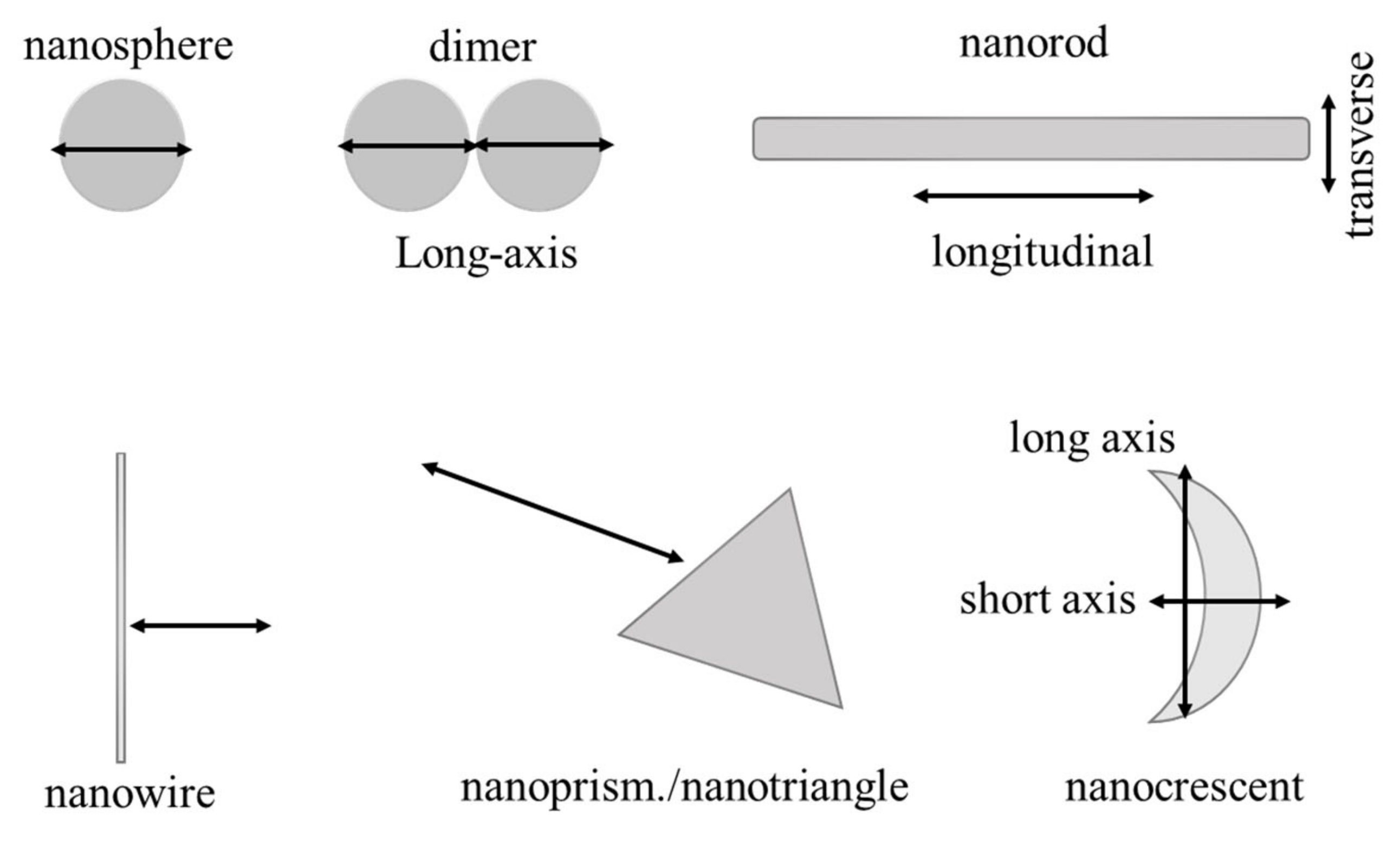
2. Tailoring between LSPR Scattering and Symmetry of Plasmonic Nanostructures
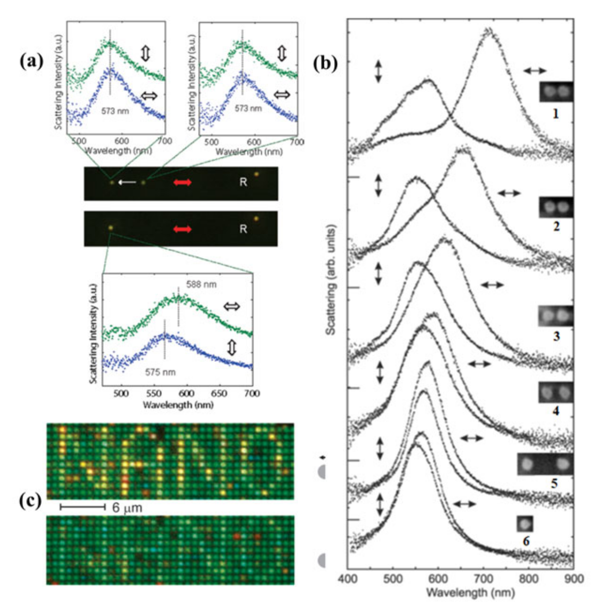
2.1. Single Nanosphere and Dimer
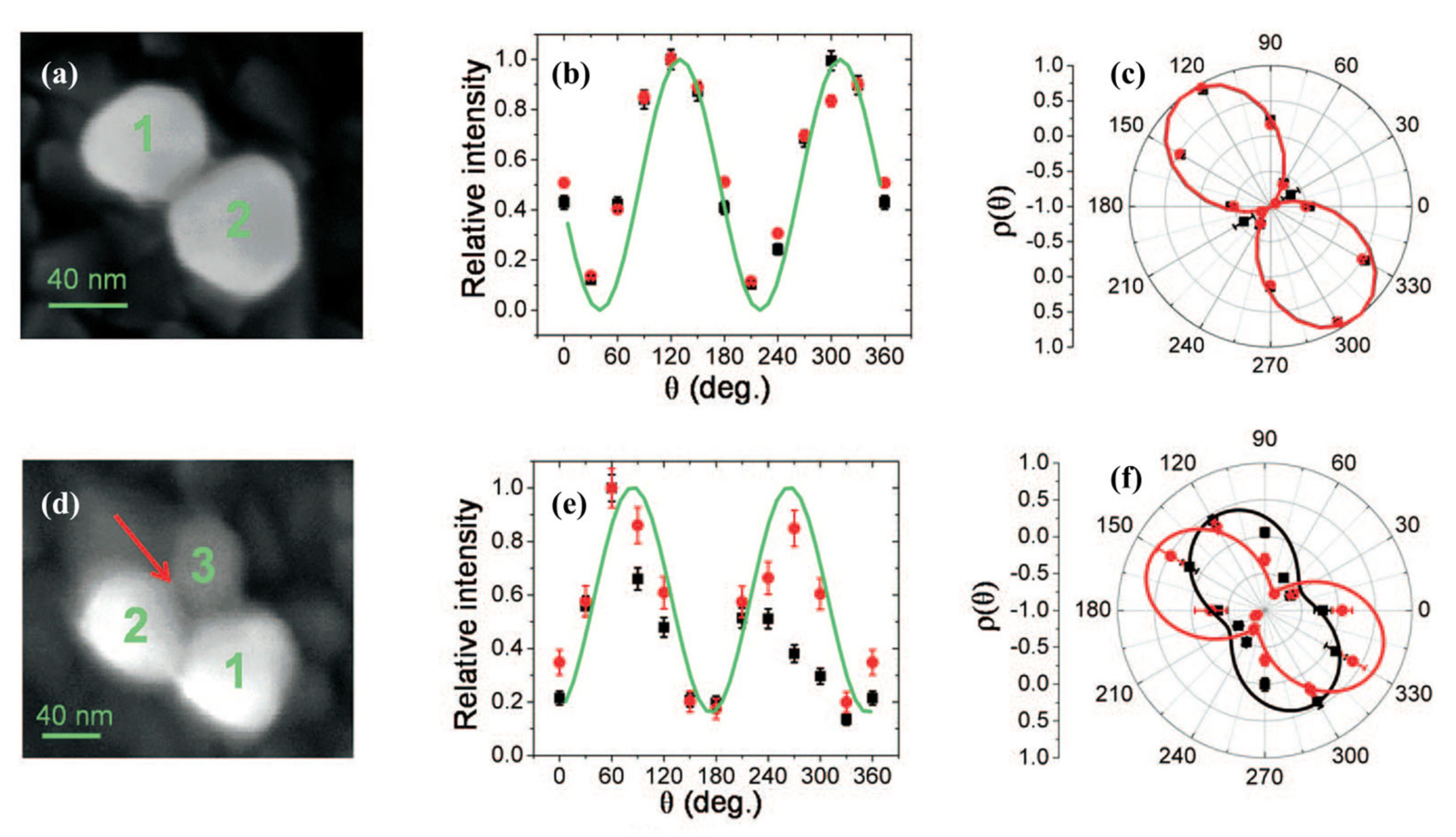
2.2. Nanosphere Trimer
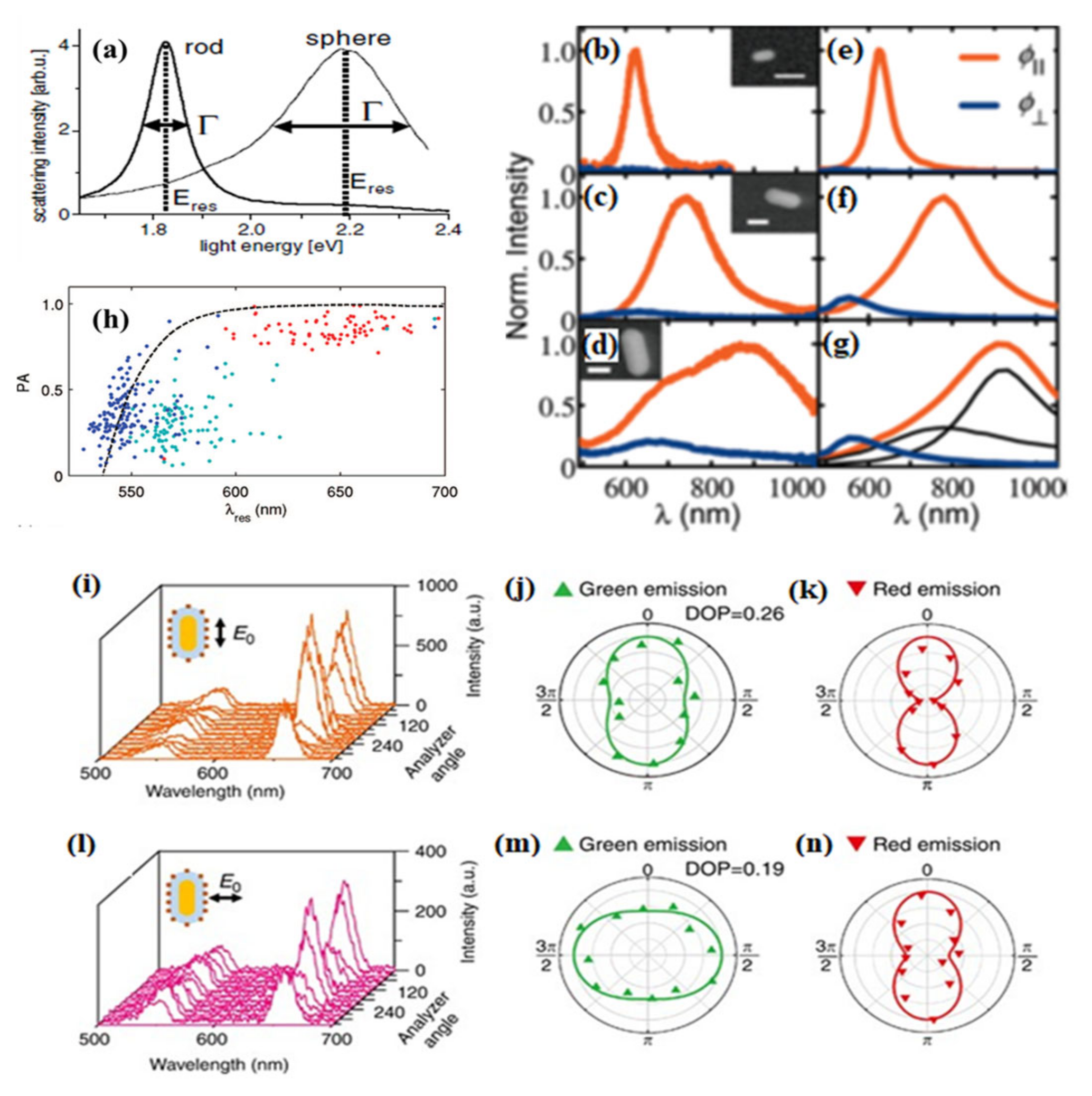
2.3. Nanorod
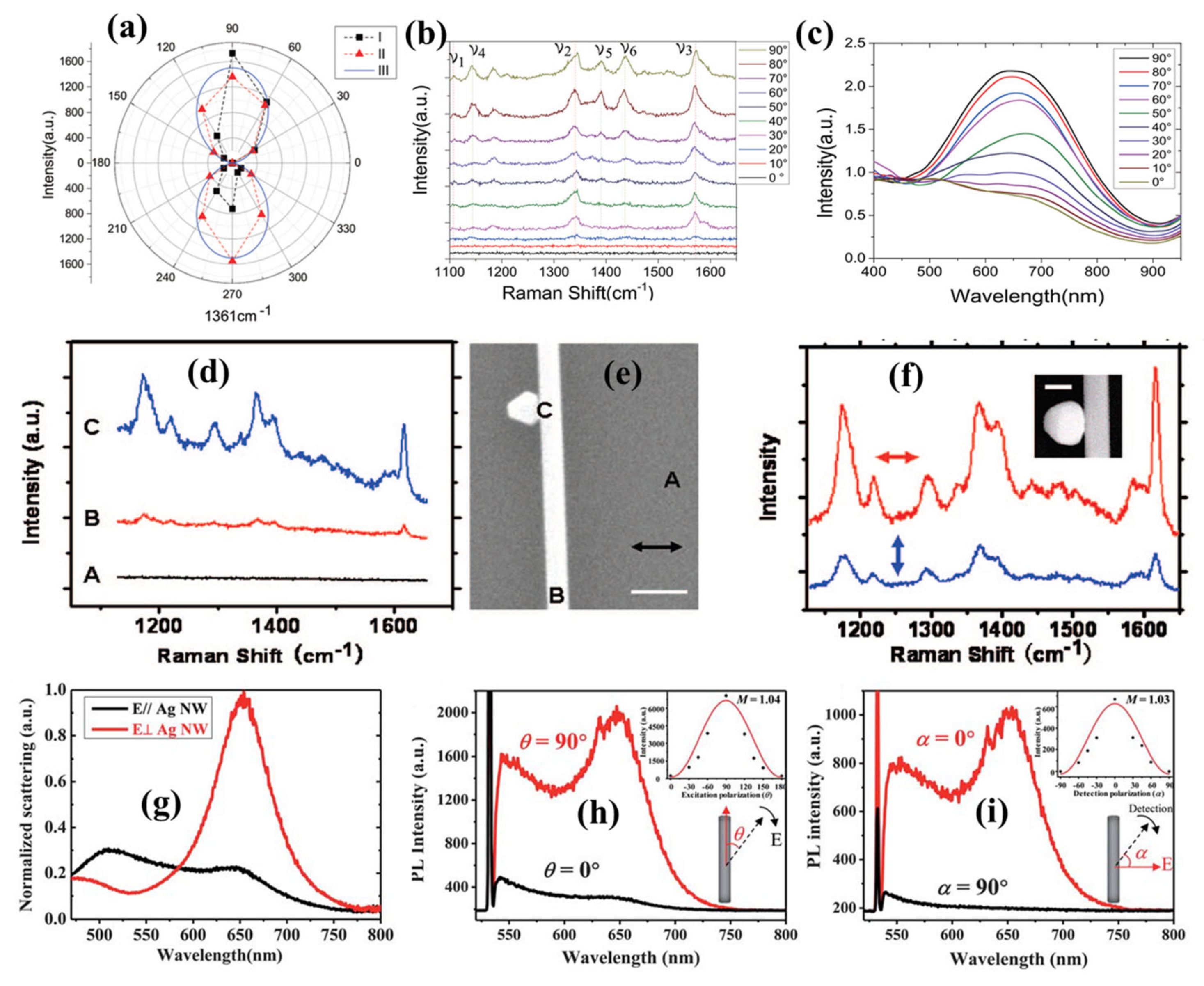
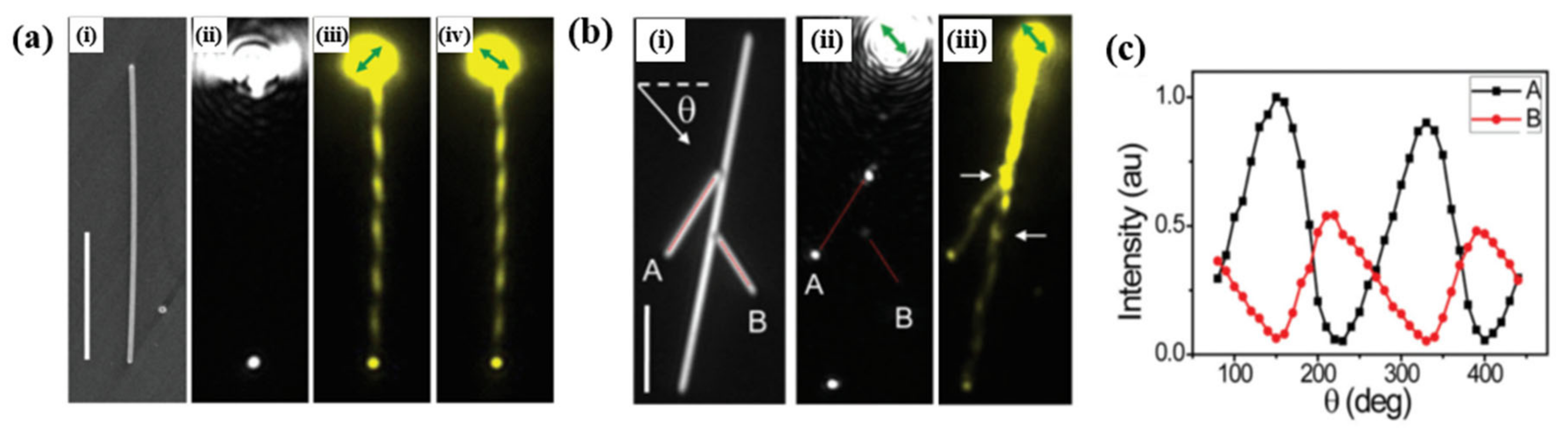
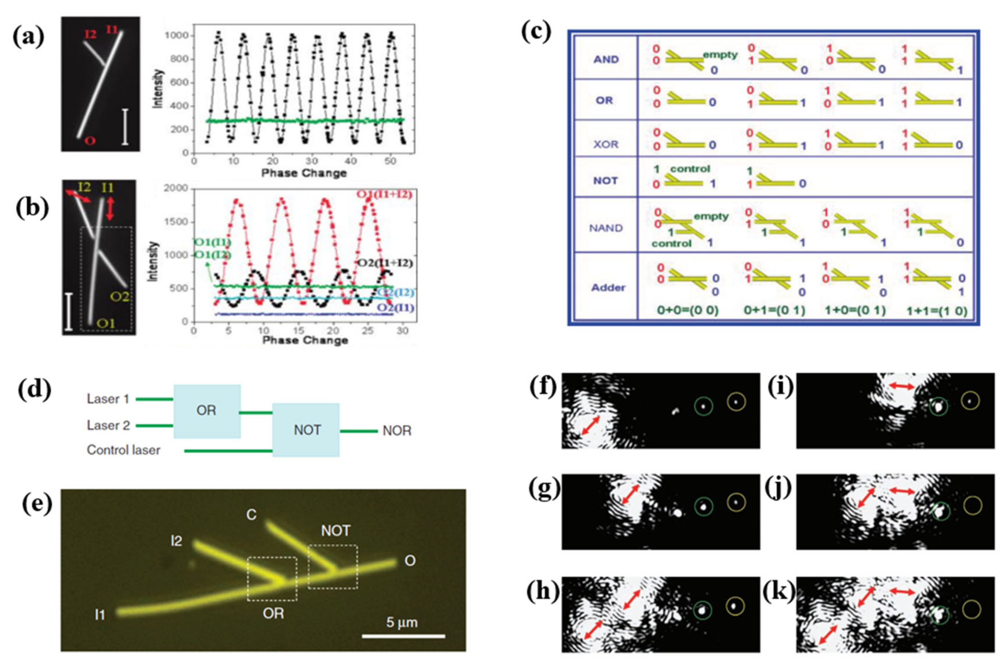
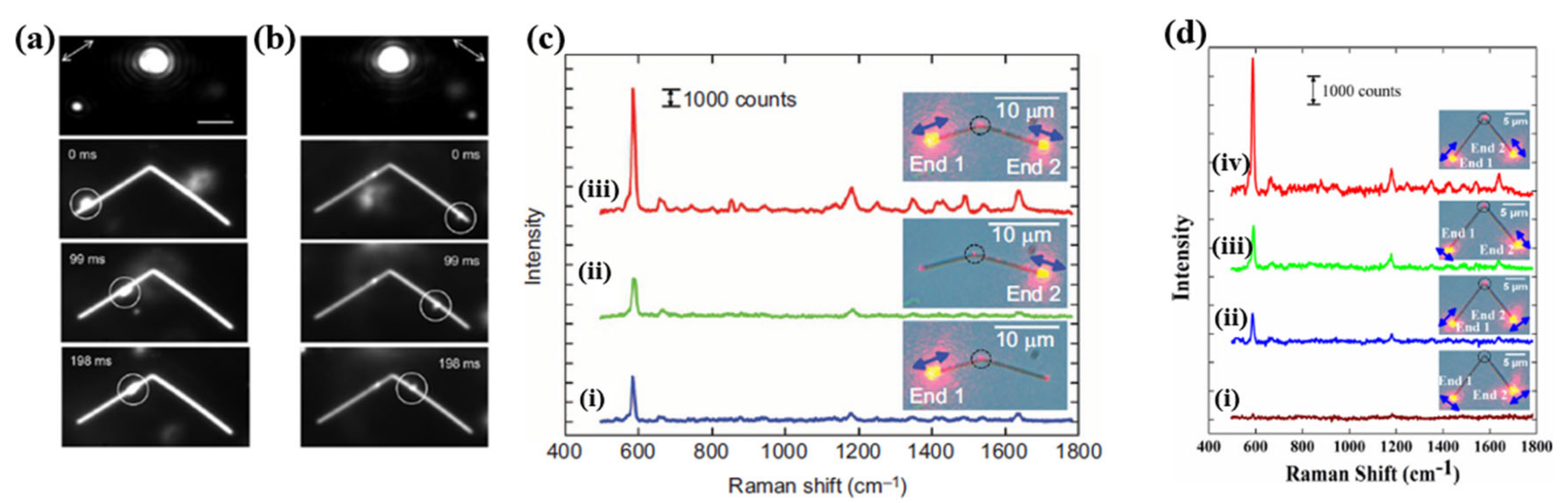
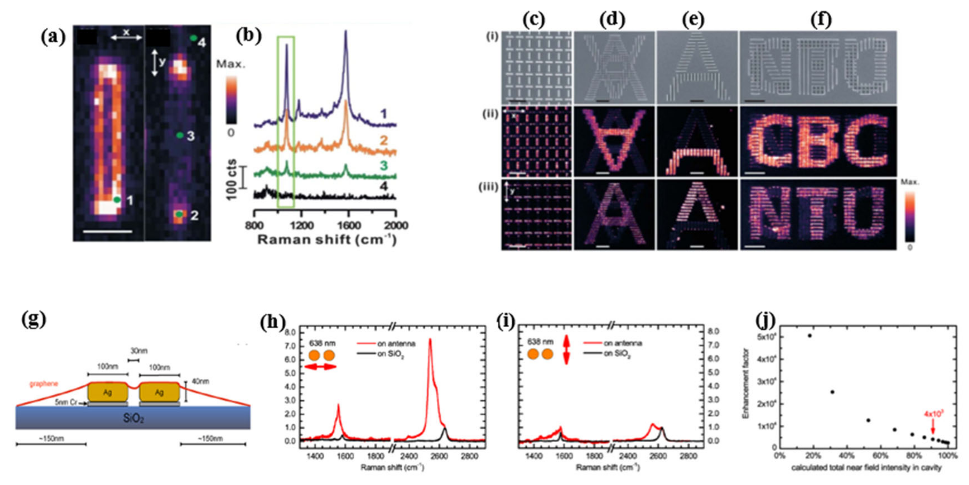
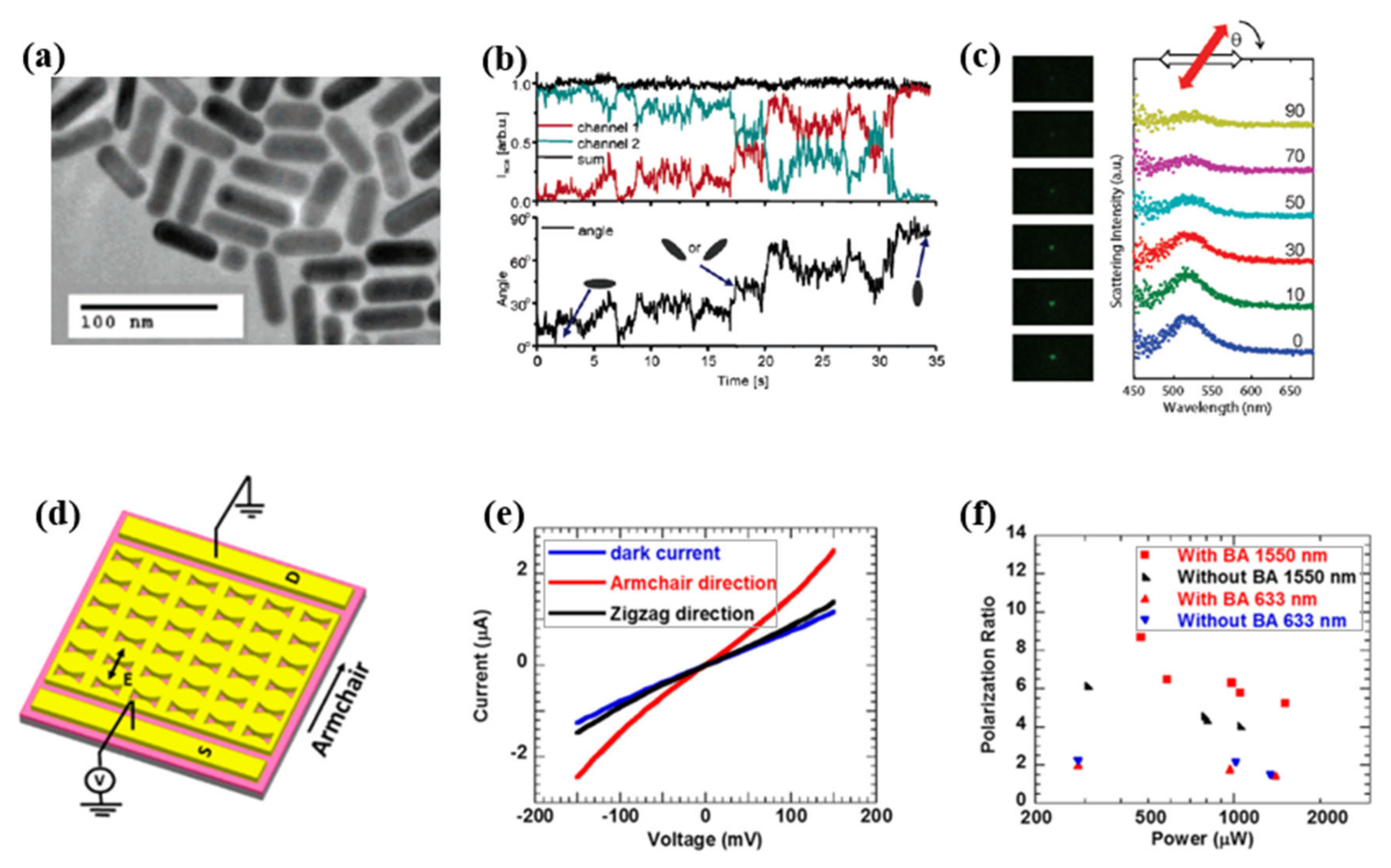
2.4. Nanowire
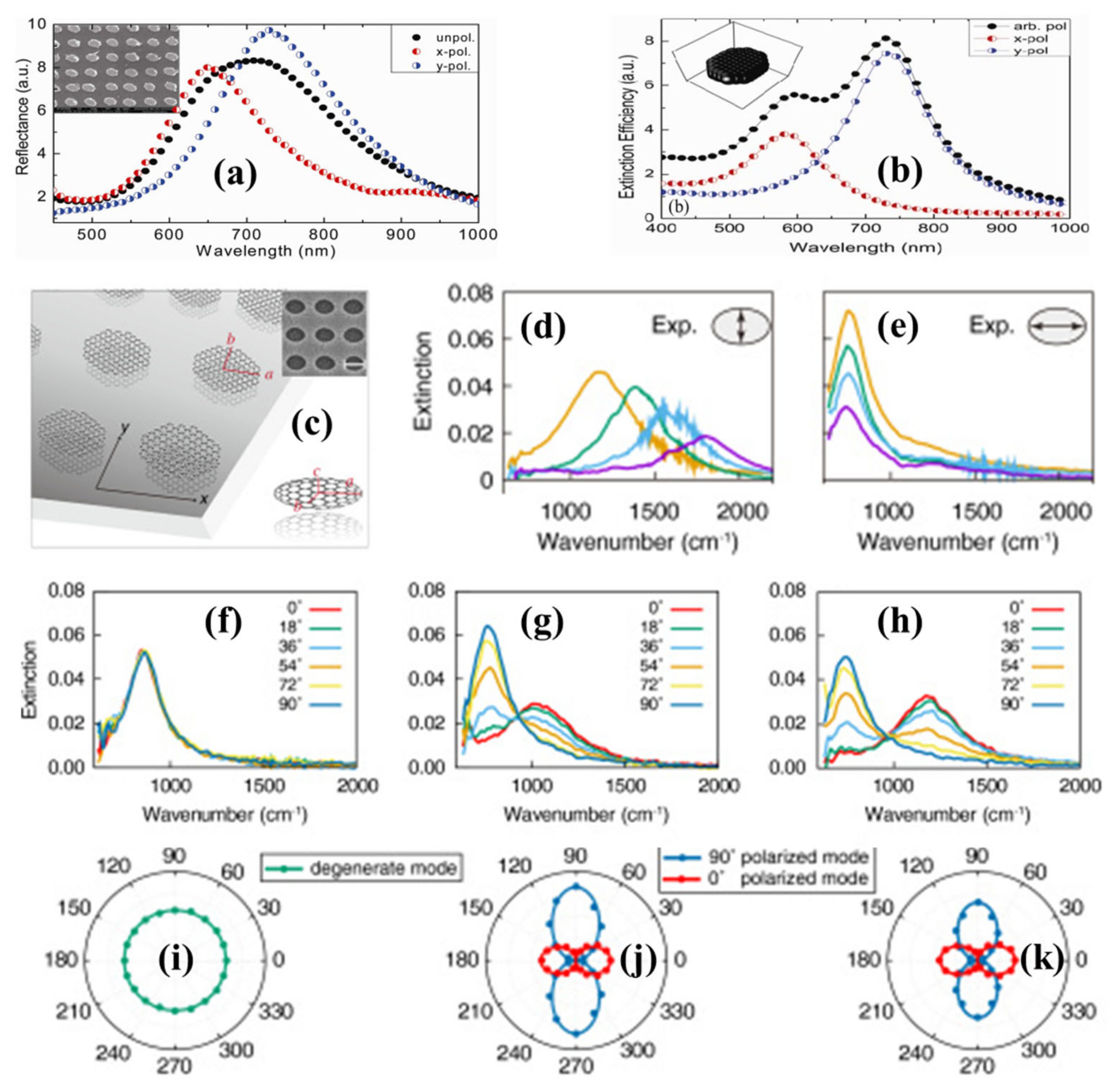
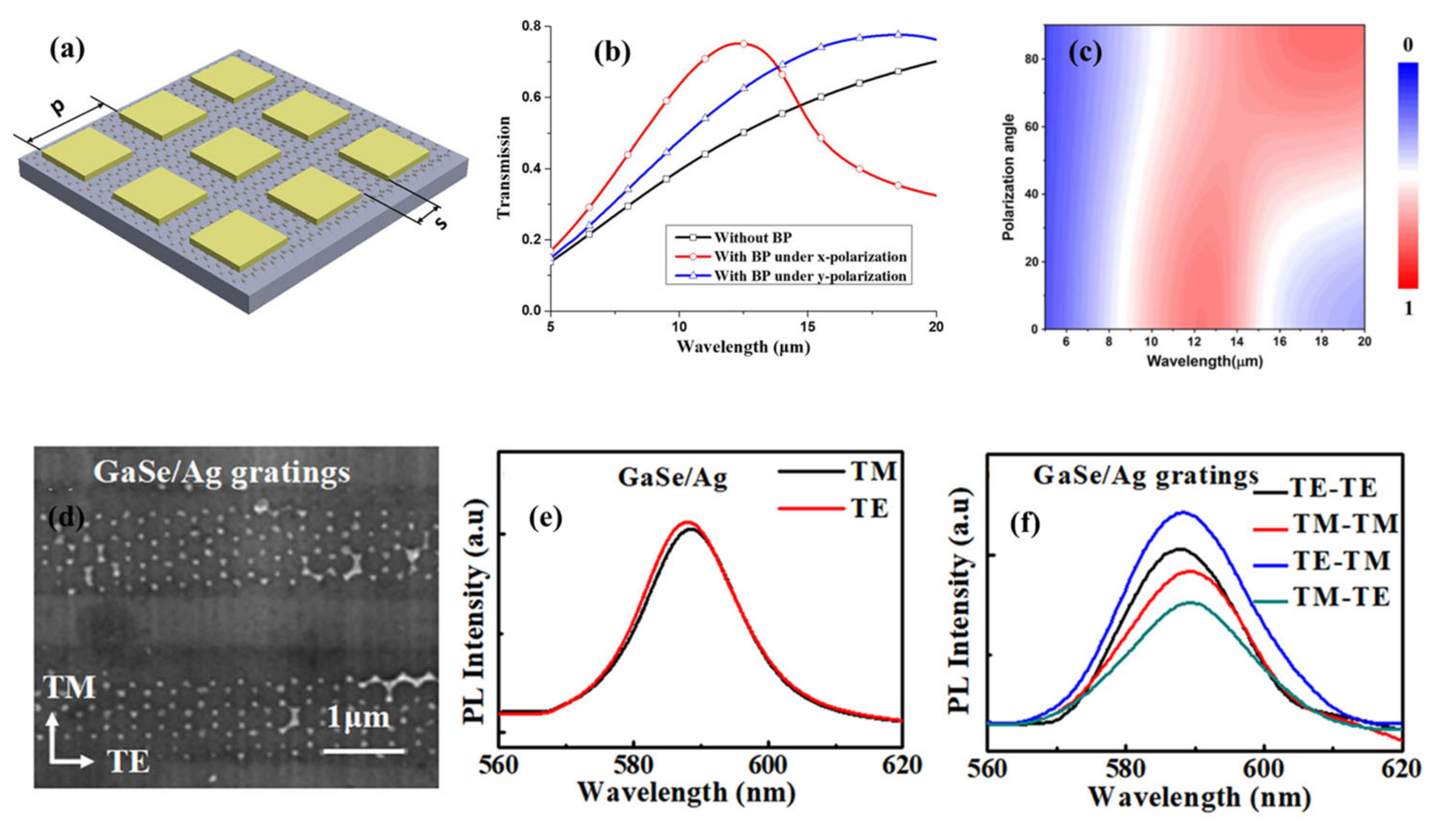
2.5. Nanohole and Nanoellipse
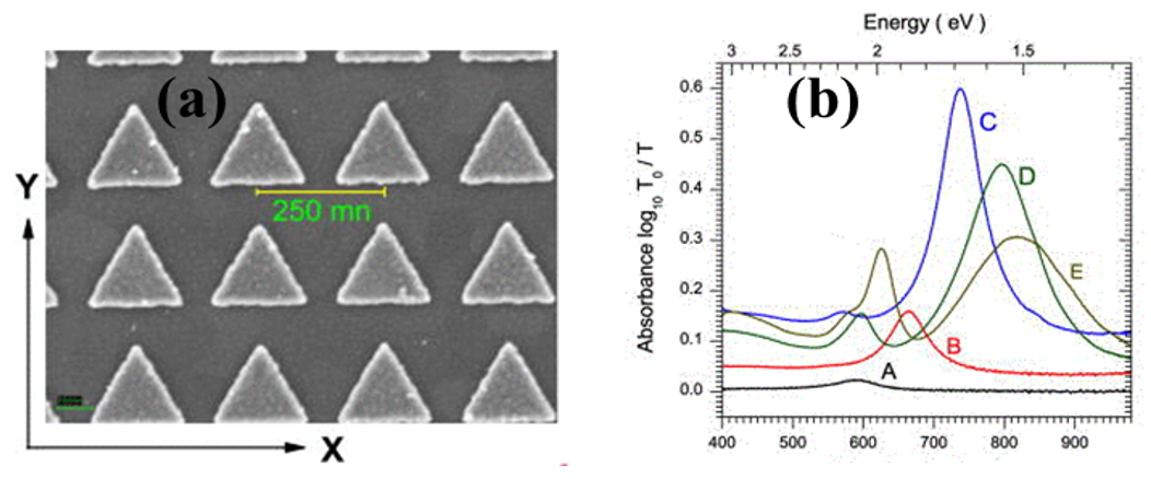
2.6. Nanoprism and Nanotriangle
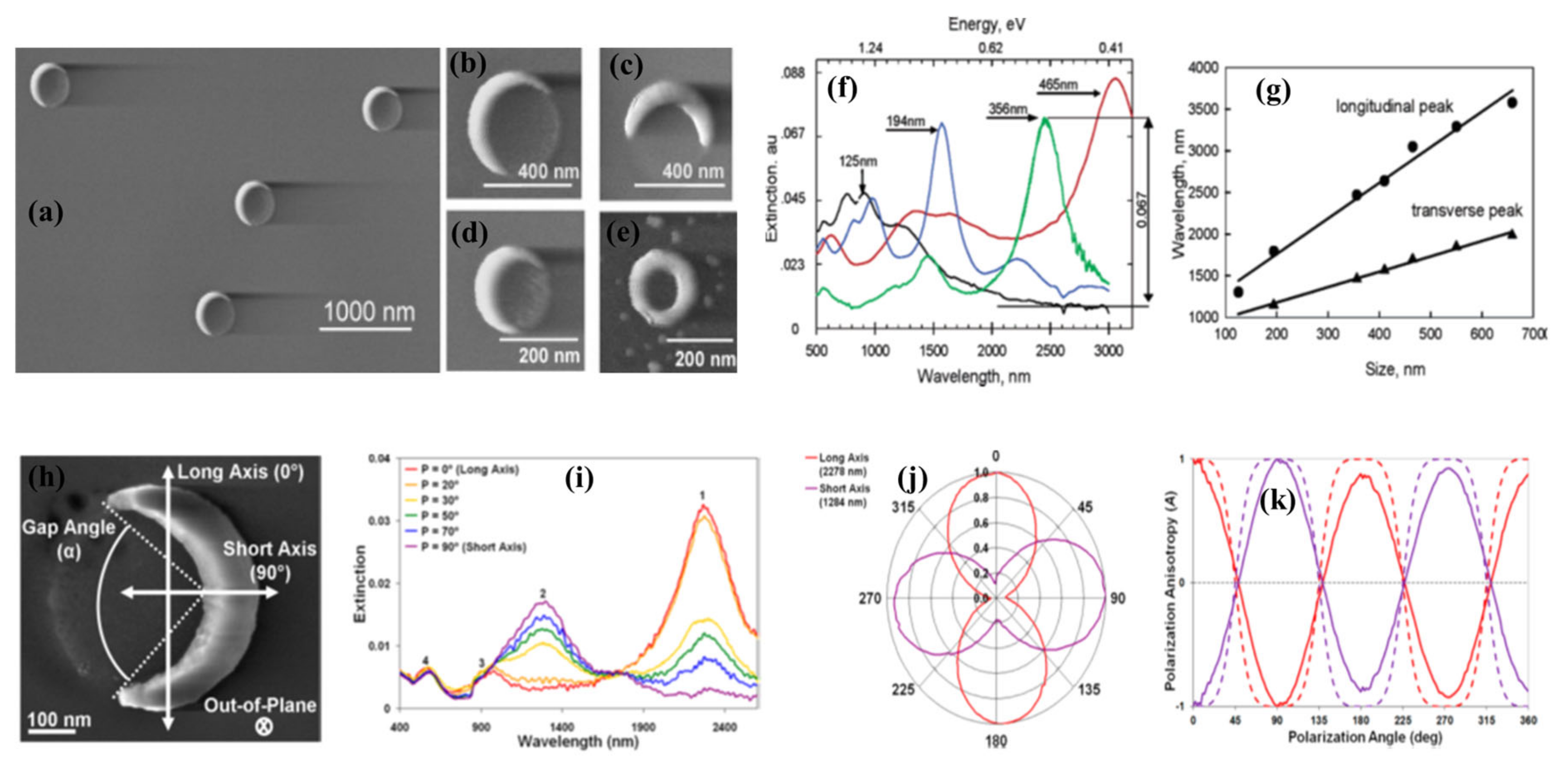
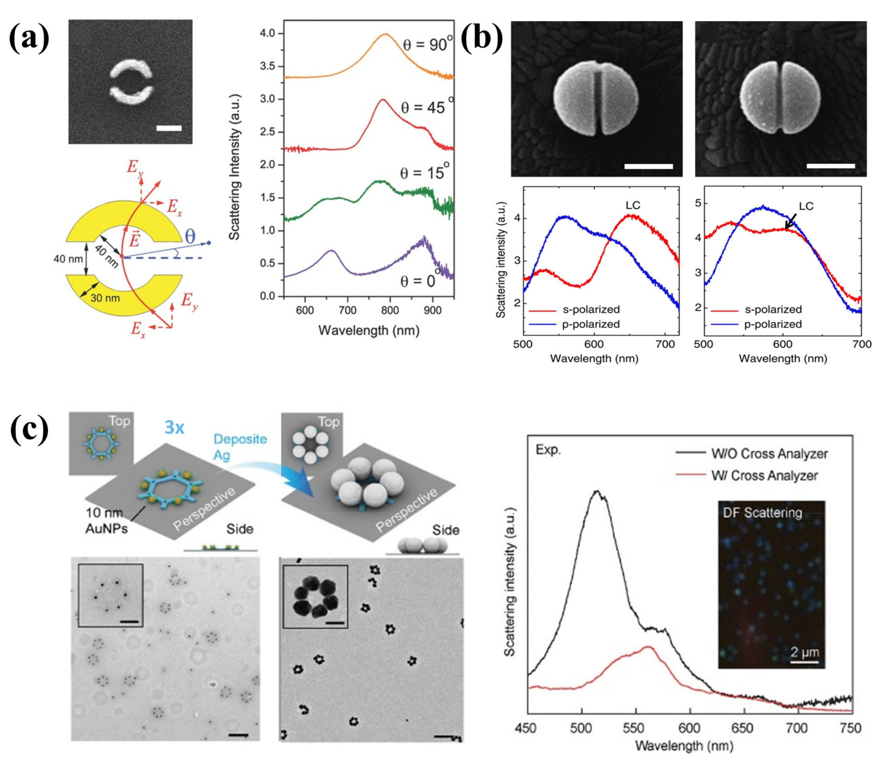
2.7. Nanocrescent
2.8. Hybrid Plasmonic Nanostructures
2.9. Selected Applications
3. Manipulating Polarisation State via Metamaterials
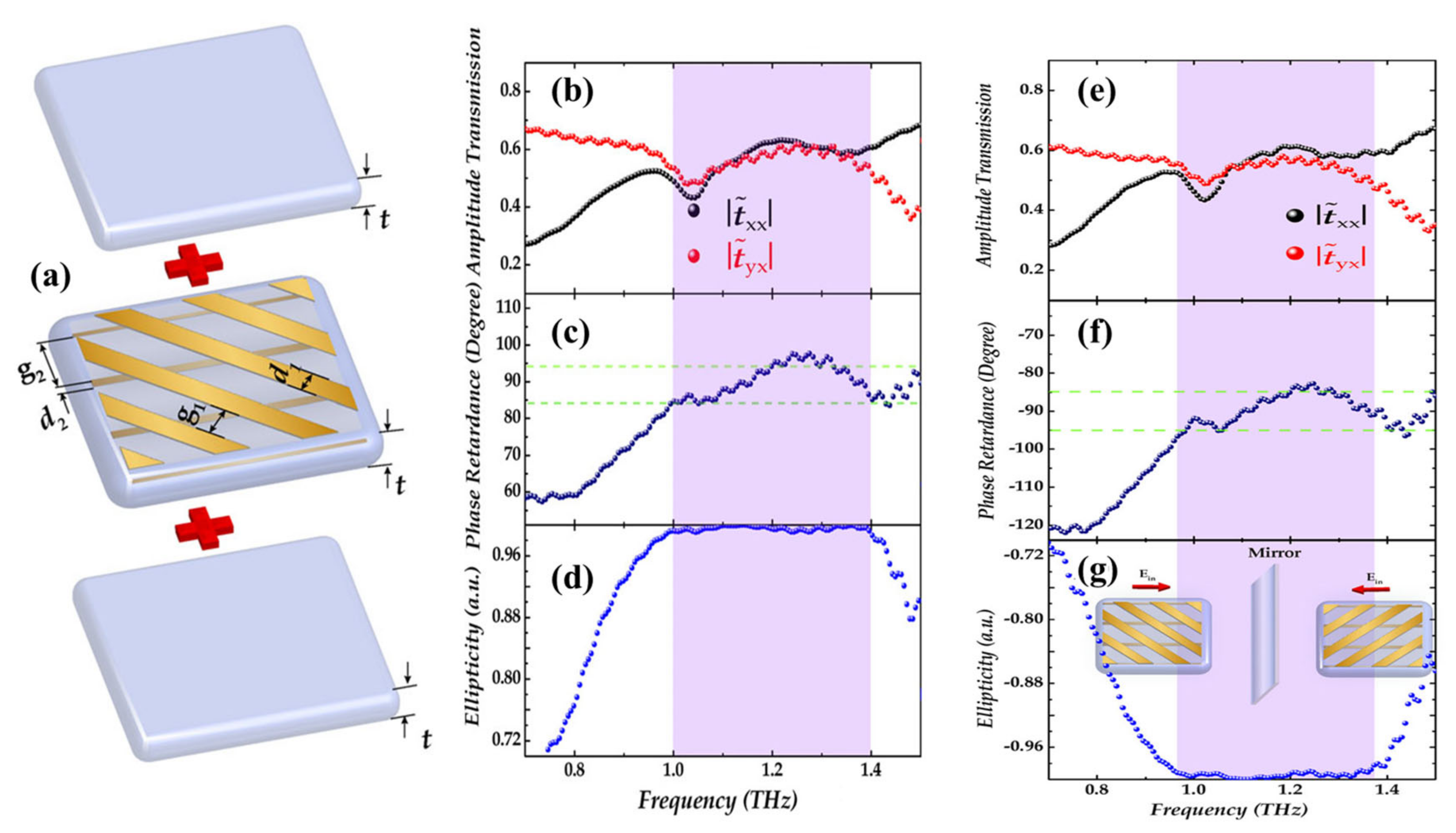
3.1. Multifunctional QWP
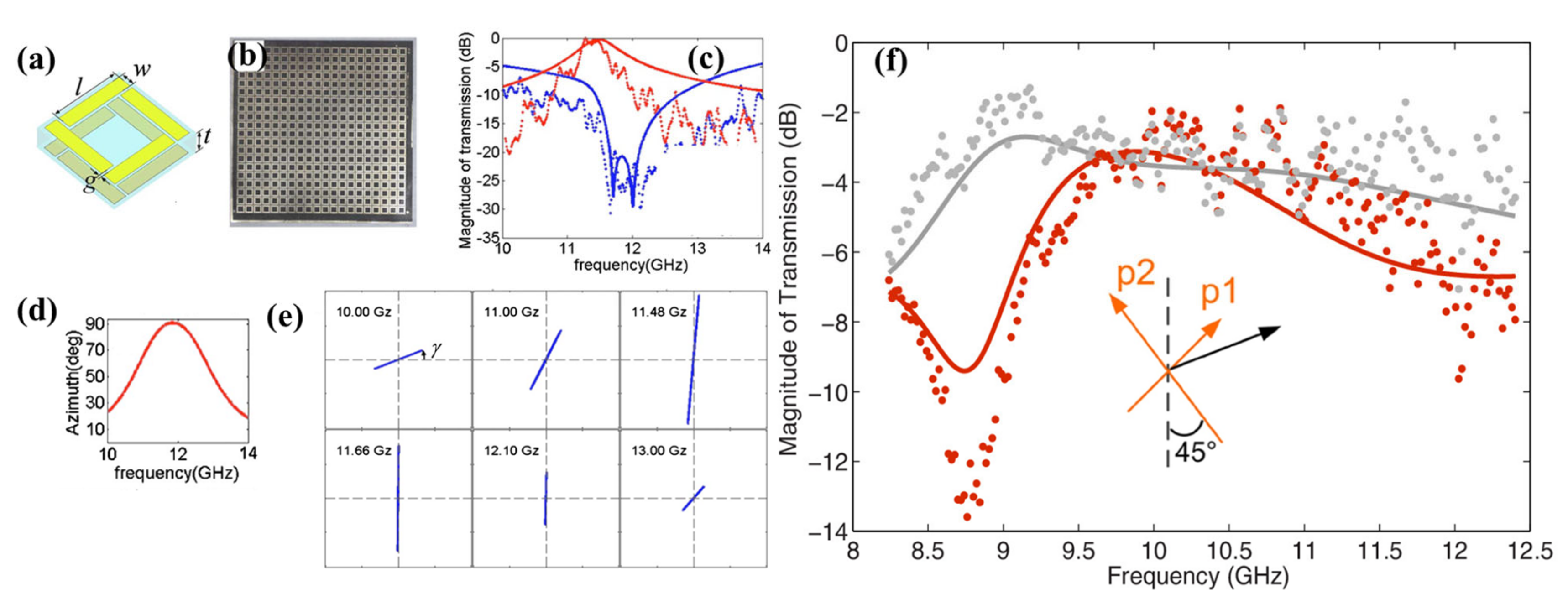
3.2. Linear to Cross Polarisation Conversion
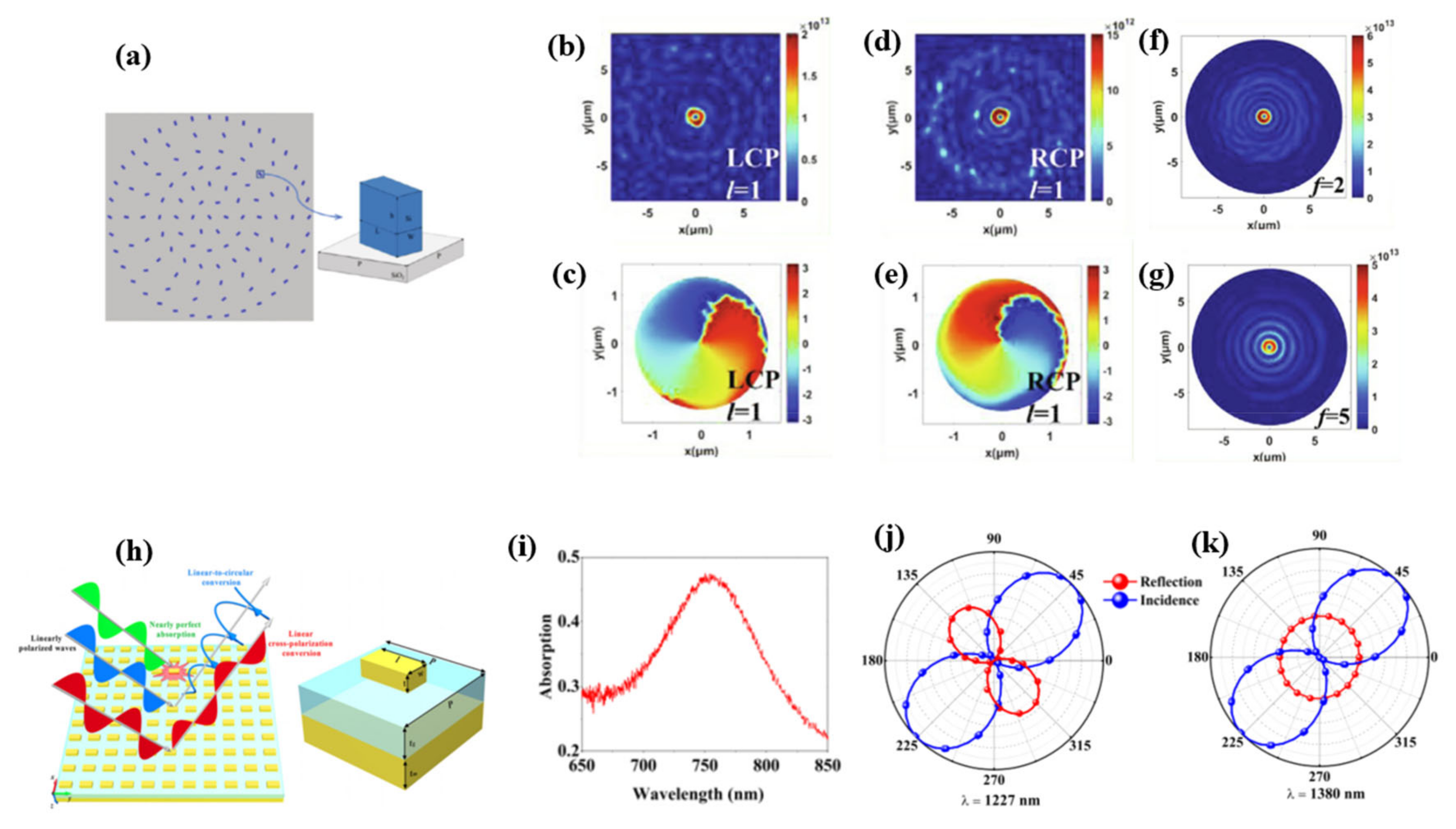
3.3. Linear to Left and Right Circular Polarisation Conversion
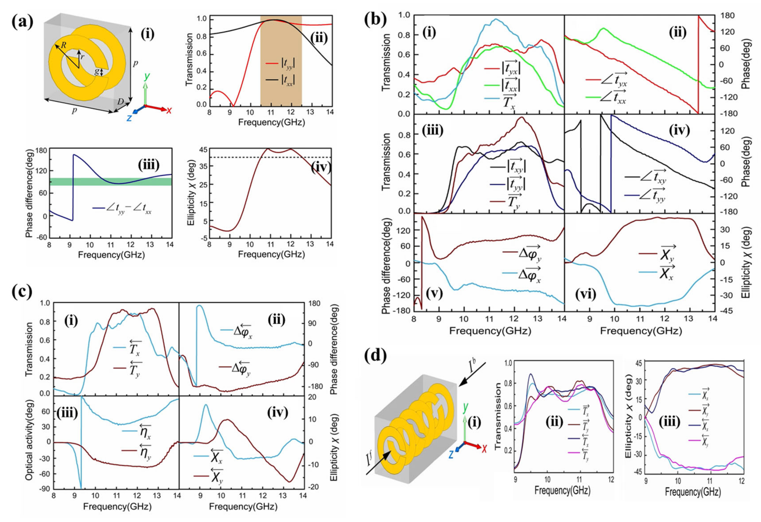
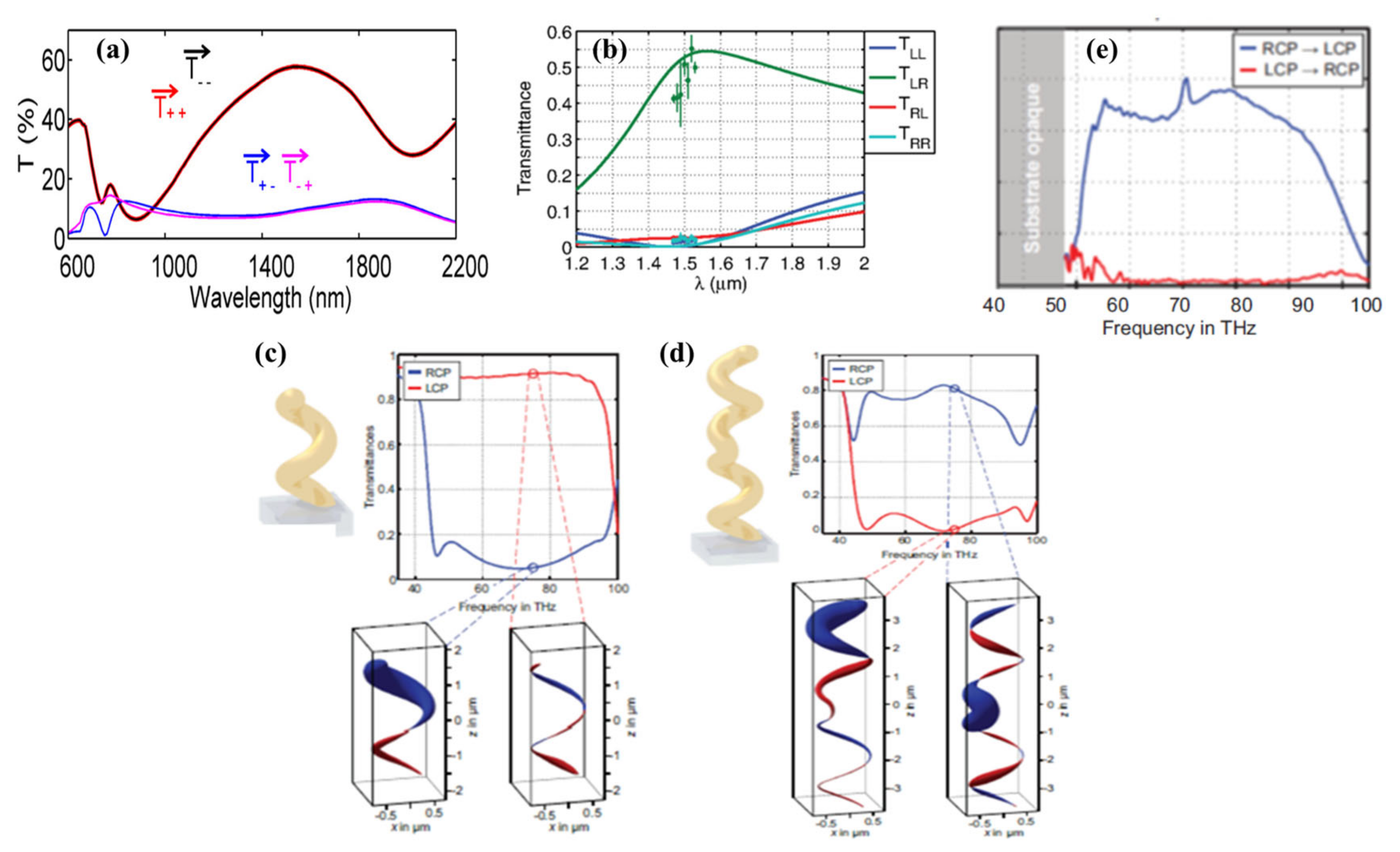
3.4. Circular Polarisation Conversion Using Helical Metamaterials
3.5. Selected Applications of Metamaterials
4. Polarisation Measurements of Magnetic-Plasmonic Nanostructures
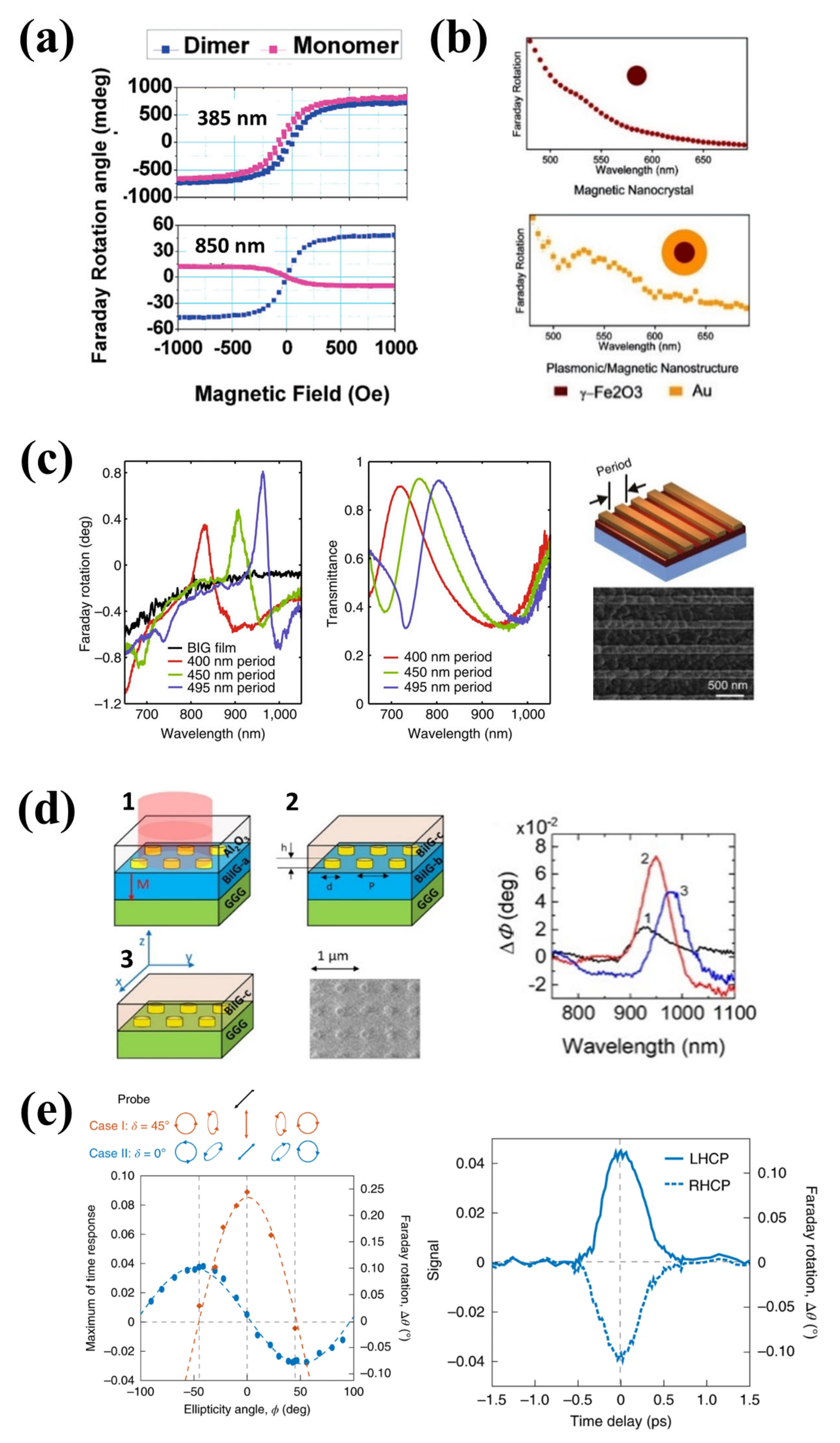
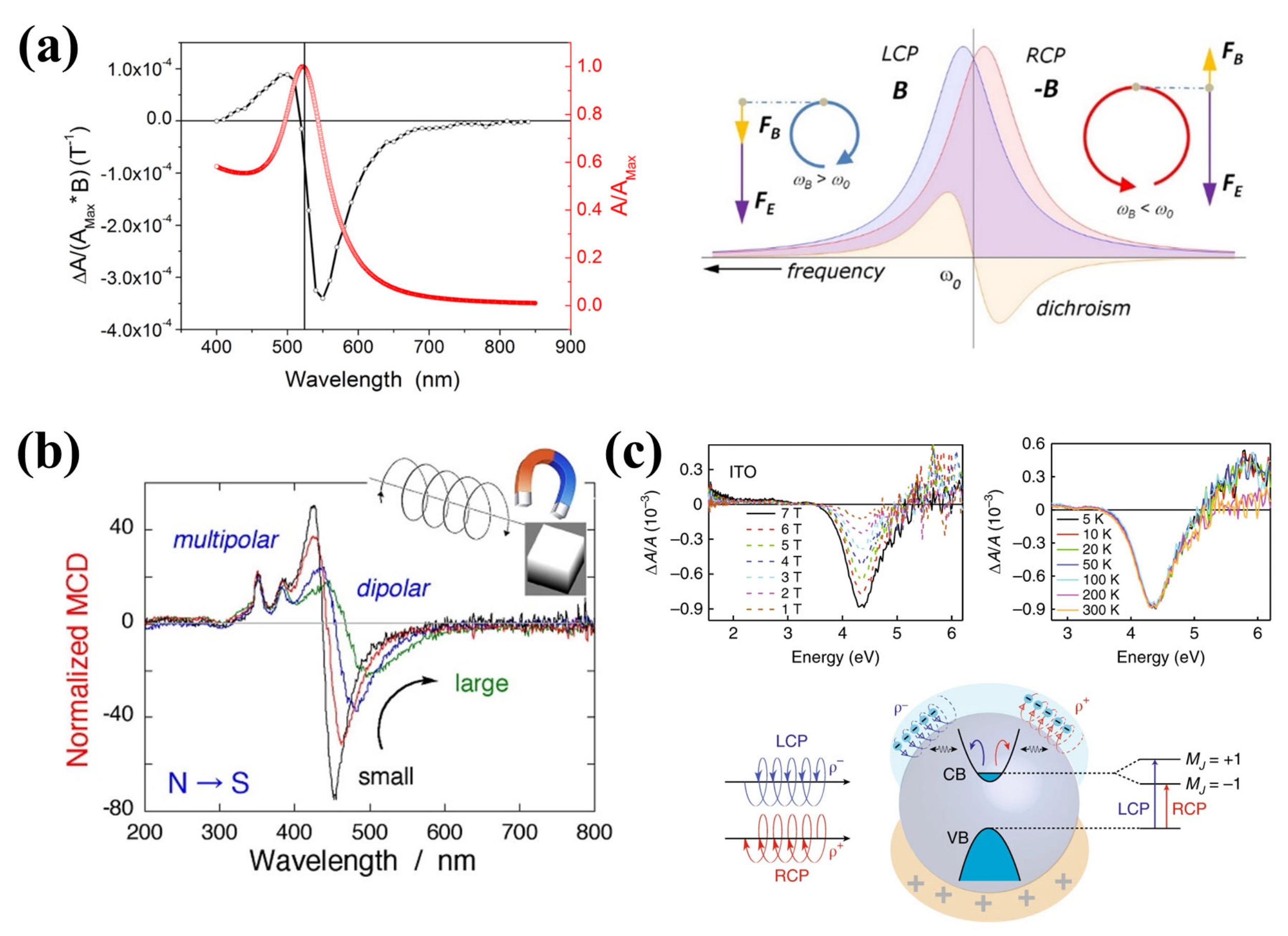
4.1. Faraday Effect and Inverse Faraday Effect
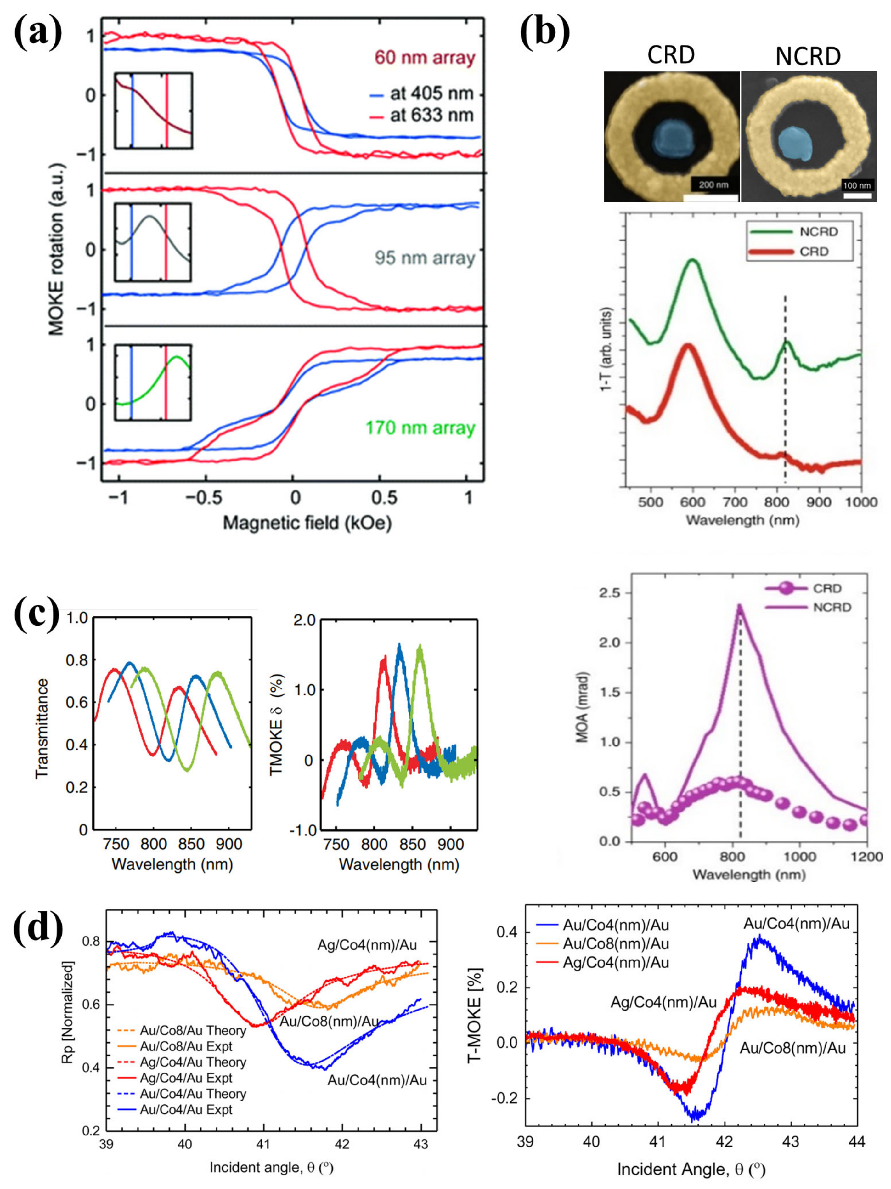
4.2. Magneto-Optic Kerr Effect
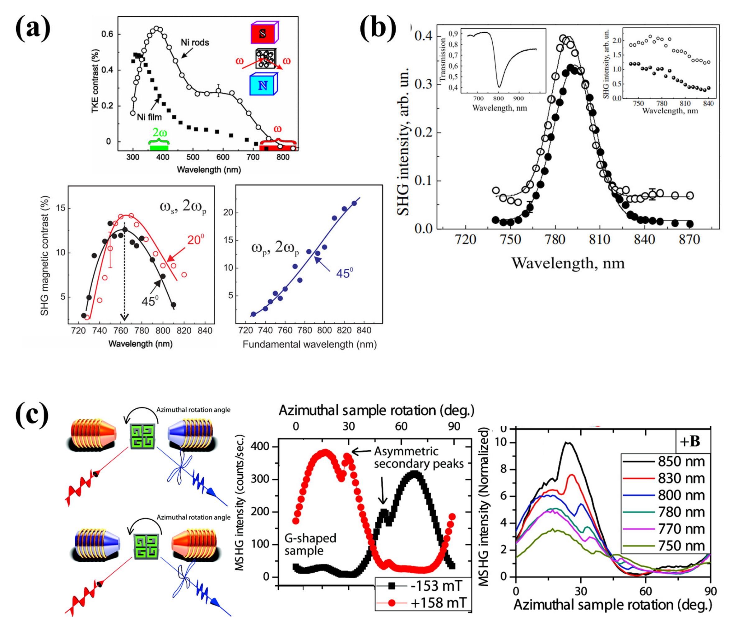
4.3. Magnetic Plasmon Resonances
4.4. Second-Harmonic Generation (SHG)
4.5. Magnetic Circular Dichroism
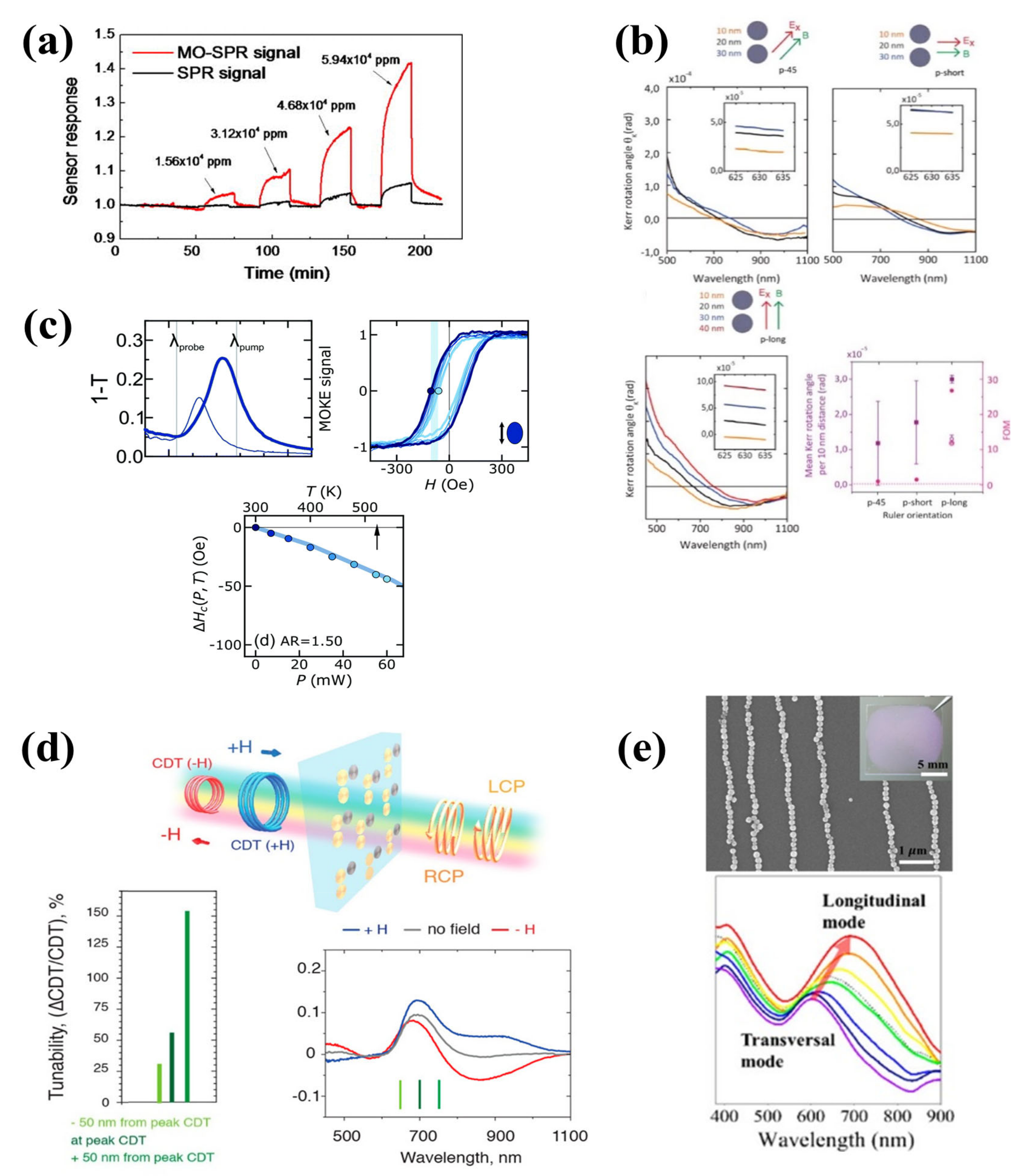
4.6. Applications of Magneto-Plasmonics
5. Conclusions and Perspectives
Author Contributions
Funding
Conflicts of Interest
References
- Jiang, N.; Zhuo, X.; Wang, J. Active Plasmonics: Principles, Structures, and Applications. Chem. Rev. 2018, 118, 3054–3099. [Google Scholar] [CrossRef] [PubMed]
- Stockman, M.I.; Kneipp, K.; Bozhevolnyi, S.I.; Saha, S.; Dutta, A.; Ndukaife, J.; Kinsey, N.; Reddy, H.; Guler, U.; Shalaev, V.M.; et al. Roadmap on plasmonics. J. Opt. 2018, 20. [Google Scholar] [CrossRef] [Green Version]
- Harutyunyan, H.; Martinson, A.B.; Rosenmann, D.; Khorashad, L.K.; Besteiro, L.V.; Govorov, A.O.; Wiederrecht, G.P. Anomalous ultrafast dynamics of hot plasmonic electrons in nanostructures with hot spots. Nat. Nanotechnol. 2015, 10, 770–774. [Google Scholar] [CrossRef]
- Baffou, G.; Quidant, R. Nanoplasmonics for chemistry. Chem. Soc. Rev. 2014, 43, 3898–3907. [Google Scholar] [CrossRef] [PubMed]
- Willets, K.A.; Van Duyne, R.P. Localized surface plasmon resonance spectroscopy and sensing. Annu. Rev. Phys. Chem. 2007, 58, 267–297. [Google Scholar] [CrossRef] [Green Version]
- Huang, W.; Wang, J.; Bian, L.; Zhao, C.; Liu, D.; Guo, C.; Yang, B.; Cao, W. Oxygen vacancy induces self-doping effect and metalloid LSPR in non-stoichiometric tungsten suboxide synergistically contributing to the enhanced photoelectrocatalytic performance of WO3-x/TiO2-x heterojunction. Phys. Chem. Chem. Phys. 2018, 20, 17268–17278. [Google Scholar] [CrossRef]
- Leonhardt, U. Optical conformal mapping. Science 2006, 312, 1777–1780. [Google Scholar] [CrossRef]
- Wei, H.; Pan, D.; Xu, H. Routing of surface plasmons in silver nanowire networks controlled by polarization and coating. Nanoscale 2015, 7, 19053–19059. [Google Scholar] [CrossRef]
- Mejia-Salazar, J.R.; Oliveira, O.N., Jr. Plasmonic Biosensing. Chem. Rev. 2018, 118, 10617–10625. [Google Scholar] [CrossRef]
- Yu, C.; Irudayaraj, J. Multiplex Biosensor Using Gold Nanorods. Anal. Chem. 2007, 79, 572–579. [Google Scholar] [CrossRef]
- Tian, F.; Bonnier, F.; Casey, A.; Shanahan, A.E.; Byrne, H.J. Surface enhanced Raman scattering with gold nanoparticles: Effect of particle shape. Anal. Methods 2014, 6, 9116–9123. [Google Scholar] [CrossRef] [Green Version]
- Ringe, E.; Langille, M.R.; Sohn, K.; Zhang, J.; Huang, J.; Mirkin, C.A.; Van Duyne, R.P.; Marks, L.D. Plasmon Length: A Universal Parameter to Describe Size Effects in Gold Nanoparticles. J. Phys. Chem. Lett. 2012, 3, 1479–1483. [Google Scholar] [CrossRef] [PubMed]
- Li, D. Femtosecond polarization switching. Nat. Photonics 2017, 11, 336–337. [Google Scholar] [CrossRef]
- Yang, Y.; Kelley, K.; Sachet, E.; Campione, S.; Luk, T.S.; Maria, J.-P.; Sinclair, M.B.; Brener, I. Femtosecond optical polarization switching using a cadmium oxide-based perfect absorber. Nat. Photonics 2017, 11, 390–395. [Google Scholar] [CrossRef]
- Schubert, O.; Becker, J.; Carbone, L.; Khalavka, Y.; Provalska, T.; Zins, I.; Sonnichsen, C. Mapping the polarization pattern of plasmon modes reveals nanoparticle symmetry. Nano Lett. 2008, 8, 2345–2350. [Google Scholar] [CrossRef]
- Kumbhar, A.S.; Kinnan, M.K.; Chumanov, G. Multipole plasmon resonances of submicron silver particles. J. Am. Chem. Soc. 2005, 127, 12444–12445. [Google Scholar] [CrossRef]
- Tian, X.; Zhou, Y.; Thota, S.; Zou, S.; Zhao, J. Plasmonic Coupling in Single Silver Nanosphere Assemblies by Polarization-Dependent Dark-Field Scattering Spectroscopy. J. Phys. Chem. C 2014, 118, 13801–13808. [Google Scholar] [CrossRef]
- Shegai, T.; Li, Z.; Dadosh, T.; Zhang, Z.; Xu, H.; Haran, G. Managing light polarization via plasmon-molecule interactions within an asymmetric metal nanoparticle trimer. Proc. Natl. Acad. Sci. USA 2008, 105, 16448–16453. [Google Scholar] [CrossRef] [Green Version]
- Luo, M.; Huang, H.; Choi, S.I.; Zhang, C.; da Silva, R.R.; Peng, H.C.; Li, Z.Y.; Liu, J.; He, Z.; Xia, Y. Facile Synthesis of Ag Nanorods with No Plasmon Resonance Peak in the Visible Region by Using Pd Decahedra of 16 nm in Size as Seeds. ACS Nano 2015, 9, 10523–10532. [Google Scholar] [CrossRef]
- Shuford, K.L.; Ratner, M.A.; Schatz, G.C. Multipolar excitation in triangular nanoprisms. J. Chem. Phys. 2005, 123, 114713. [Google Scholar] [CrossRef]
- Felidj, N.; Grand, J.; Laurent, G.; Aubard, J.; Levi, G.; Hohenau, A.; Galler, N.; Aussenegg, F.R.; Krenn, J.R. Multipolar surface plasmon peaks on gold nanotriangles. J. Chem. Phys. 2008, 128, 094702. [Google Scholar] [CrossRef] [PubMed]
- Bukasov, R.; Shumaker-Parry, J.S. Highly tunable infrared extinction properties of gold nanocrescents. Nano Lett. 2007, 7, 1113–1118. [Google Scholar] [CrossRef] [PubMed]
- Li, G.C.; Zhang, Y.L.; Lei, D.Y. Hybrid plasmonic gap modes in metal film-coupled dimers and their physical origins revealed by polarization resolved dark field spectroscopy. Nanoscale 2016, 8, 7119–7126. [Google Scholar] [CrossRef] [PubMed] [Green Version]
- Chen, W.; Shi, H.; Wan, F.; Wang, P.; Gu, Z.; Li, W.; Ke, L.; Huang, Y. Substrate influence on the polarization dependence of SERS in crossed metal nanowires. J. Mater. Chem. C 2017, 5, 7028–7034. [Google Scholar] [CrossRef]
- Wei, H.; Hao, F.; Huang, Y.; Wang, W.; Nordlander, P.; Xu, H. Polarization dependence of surface-enhanced Raman scattering in gold nanoparticle-nanowire systems. Nano Lett. 2008, 8, 2497–2502. [Google Scholar] [CrossRef]
- Deng, G.; Dereshgi, S.A.; Song, X.; Aydin, K. Polarization dependent, plasmon-enhanced infrared transmission through gold nanoslits on monolayer black phosphorus. J. Opt. Soc. Am. B 2019, 36. [Google Scholar] [CrossRef]
- Liu, C.; Bai, Y.; Zhou, J.; Zhao, Q.; Yang, Y.; Chen, H.; Qiao, L. High-performance bifunctional polarization switch chiral metamaterials by inverse design method. npj Comput. Mater. 2019, 5. [Google Scholar] [CrossRef] [Green Version]
- Kaschke, J.; Blume, L.; Wu, L.; Thiel, M.; Bade, K.; Yang, Z.; Wegener, M. A Helical Metamaterial for Broadband Circular Polarization Conversion. Adv. Opt. Mater. 2015, 3, 1411–1417. [Google Scholar] [CrossRef]
- Kruk, S.; Hopkins, B.; Kravchenko, I.I.; Miroshnichenko, A.; Neshev, D.N.; Kivshar, Y.S. Invited Article: Broadband highly efficient dielectric metadevices for polarization control. APL Photonics 2016, 1. [Google Scholar] [CrossRef] [Green Version]
- Chen, S.; Liu, W.; Li, Z.; Cheng, H.; Tian, J. Polarization State Manipulation of Electromagnetic Waves with Metamaterials and Its Applications in Nanophotonics. In Metamaterials—Devices and Applications; IntechOpen Limited: London, UK, 2017. [Google Scholar] [CrossRef] [Green Version]
- Bi, K.; Yang, D.; Chen, J.; Wang, Q.; Wu, H.; Lan, C.; Yang, Y. Experimental demonstration of ultra-large-scale terahertz all-dielectric metamaterials. Photonics Res. 2019, 7, 457–463. [Google Scholar] [CrossRef]
- Soukoulis, C.M.; Wegener, M. Past achievements and future challenges in the development of three-dimensional photonic metamaterials. Nat. Photonics 2011, 5, 523–530. [Google Scholar] [CrossRef] [Green Version]
- Tong, L.; Miljkovic, V.D.; Kall, M. Alignment, rotation, and spinning of single plasmonic nanoparticles and nanowires using polarization dependent optical forces. Nano Lett. 2010, 10, 268–273. [Google Scholar] [CrossRef] [PubMed]
- Gunnarsson, L.; Rindzevicius, T.; Prikulis, J.; Kasemo, B.; Kall, M.; Zou, S.; Schatz, G.C. Confined plasmons in nanofabricated single silver particle pairs: Experimental observations of strong interparticle interactions. J. Phys. Chem. B 2005, 109, 1079–1087. [Google Scholar] [CrossRef] [PubMed]
- Dort, K.; Kroth, K.; Klar, P.J. A surface-enhanced Raman-spectroscopic study: Verification of the interparticle gap dependence of field enhancement by triangulation of spherical gold nanoparticle trimers. J. Raman Spectrosc. 2019, 50, 1807–1816. [Google Scholar] [CrossRef] [Green Version]
- Steinigeweg, D.; Schutz, M.; Schlucker, S. Single gold trimers and 3D superstructures exhibit a polarization-independent SERS response. Nanoscale 2013, 5, 110–113. [Google Scholar] [CrossRef]
- Wang, H.; Li, Z.; Zhang, H.; Wang, P.; Wen, S. Giant local circular dichroism within an asymmetric plasmonic nanoparticle trimer. Sci. Rep. 2015, 5, 8207. [Google Scholar] [CrossRef]
- Mohamed, M.B.; Volkov, V.; Link, S.; El-Sayed, M.A. The ‘lightning’ gold nanorods: Fluorescence enhancement of over a million compared to the gold metal. Chem. Phys. Lett. 2000, 317, 517–523. [Google Scholar] [CrossRef]
- Sonnichsen, C.; Franzl, T.; Wilk, T.; von Plessen, G.; Feldmann, J.; Wilson, O.; Mulvaney, P. Drastic reduction of plasmon damping in gold nanorods. Phys. Rev. Lett. 2002, 88, 077402. [Google Scholar] [CrossRef]
- Slaughter, L.S.; Chang, W.-S.; Swanglap, P.; Tcherniak, A.; Khanal, B.P.; Zubarev, E.R.; Link, S. Single-Particle Spectroscopy of Gold Nanorods beyond the Quasi-Static Limit: Varying the Width at Constant Aspect Ratio. J. Phys. Chem. C 2010, 114, 4934–4938. [Google Scholar] [CrossRef]
- He, J.; Zheng, W.; Ligmajer, F.; Chan, C.F.; Bao, Z.; Wong, K.L.; Chen, X.; Hao, J.; Dai, J.; Yu, S.F.; et al. Plasmonic enhancement and polarization dependence of nonlinear upconversion emissions from single gold nanorod@SiO2@CaF2:Yb(3+),Er(3+) hybrid core-shell-satellite nanostructures. Light Sci. Appl. 2017, 6, e16217. [Google Scholar] [CrossRef]
- Khlebtsov, B.N.; Khlebtsov, N.G. Multipole Plasmons in Metal Nanorods: Scaling Properties and Dependence on Particle Size, Shape, Orientation, and Dielectric Environment. J. Phys. Chem. C 2007, 111, 11516–11527. [Google Scholar] [CrossRef]
- Aizpurua, J.; Bryant, G.W.; Richter, L.J.; García de Abajo, F.J.; Kelley, B.K.; Mallouk, T. Optical properties of coupled metallic nanorods for field-enhanced spectroscopy. Phys. Rev. B 2005, 71, 235420. [Google Scholar] [CrossRef] [Green Version]
- Ming, T.; Zhao, L.; Yang, Z.; Chen, H.; Sun, L.; Wang, J.; Yan, C. Strong polarization dependence of plasmon-enhanced fluorescence on single gold nanorods. Nano Lett. 2009, 9, 3896–3903. [Google Scholar] [CrossRef] [PubMed]
- Yguerabide, J.; Yguerabide, E.E. Light-Scattering Submicroscopic Particles as Highly Fluorescent Analogs and Their Use as Tracer Labels in Clinical and Biological Applications: I. Theory. Anal. Biochem. 1998, 262, 137–156. [Google Scholar] [CrossRef]
- Zijlstra, P.; Chon, J.W.; Gu, M. Five-dimensional optical recording mediated by surface plasmons in gold nanorods. Nature 2009, 459, 410–413. [Google Scholar] [CrossRef]
- Diefenbach, S.; Erhard, N.; Schopka, J.; Martin, A.; Karnetzky, C.; Iacopino, D.; Holleitner, A.W. Polarization dependent, surface plasmon induced photoconductance in gold nanorod arrays. Phys. Status Solidi (RRL)—Rapid Res. Lett. 2014, 8, 264–268. [Google Scholar] [CrossRef] [Green Version]
- Ruan, Q.; Fang, C.; Jiang, R.; Jia, H.; Lai, Y.; Wang, J.; Lin, H.Q. Highly enhanced transverse plasmon resonance and tunable double Fano resonances in gold@titania nanorods. Nanoscale 2016, 8, 6514–6526. [Google Scholar] [CrossRef]
- Zhang, M.; Li, C.; Wang, C.; Zhang, C.; Wang, Z.; Han, Q.; Zheng, H. Polarization dependence of plasmon enhanced fluorescence on Au nanorod array. Appl. Opt. 2017, 56, 375–379. [Google Scholar] [CrossRef] [PubMed]
- Sun, M.; Zhang, Z.; Wang, P.; Li, Q.; Ma, F.; Xu, H. Remotely excited Raman optical activity using chiral plasmon propagation in Ag nanowires. Light Sci. Appl. 2013, 2, e112. [Google Scholar] [CrossRef]
- Kim, S.; Bailey, S.; Liu, M.; Yan, R. Decoupling co-existing surface plasmon polariton (SPP) modes in a nanowire plasmonic waveguide for quantitative mode analysis. Nano Res. 2017, 10, 2395–2404. [Google Scholar] [CrossRef]
- Vasista, A.B.; Jog, H.; Heilpern, T.; Sykes, M.E.; Tiwari, S.; Sharma, D.K.; Chaubey, S.K.; Wiederrecht, G.P.; Gray, S.K.; Kumar, G.V.P. Differential Wavevector Distribution of Surface-Enhanced Raman Scattering and Fluorescence in a Film-Coupled Plasmonic Nanowire Cavity. Nano Lett. 2018, 18, 650–655. [Google Scholar] [CrossRef] [PubMed]
- Zhang, Z.; Fang, Y.; Wang, W.; Chen, L.; Sun, M. Propagating Surface Plasmon Polaritons: Towards Applications for Remote-Excitation Surface Catalytic Reactions. Adv. Sci. (Weinh) 2016, 3, 1500215. [Google Scholar] [CrossRef] [PubMed]
- Mohanty, P.; Yoon, I.; Kang, T.; Seo, K.; Varadwaj, K.S.K.; Choi, W.; Park, Q.H.; Ahn, J.P.; Suh, Y.D.; Ihee, H.; et al. Simple Vapor-Phase Synthesis of Single-Crystalline Ag Nanowires and Single-Nanowire Surface-Enhanced Raman Scattering. J. Am. Chem. Soc. 2007, 129, 9576–9577. [Google Scholar] [CrossRef] [PubMed] [Green Version]
- Li, Z.; Gao, Y.; Zhang, L.; Fang, Y.; Wang, P. Polarization-dependent surface plasmon-driven catalytic reaction on a single nanowire monitored by SERS. Nanoscale 2018, 10, 18720–18727. [Google Scholar] [CrossRef] [PubMed]
- Hao, F.; Nordlander, P. Plasmonic coupling between a metallic nanosphere and a thin metallic wire. Appl. Phys. Lett. 2006, 89, 103101. [Google Scholar] [CrossRef]
- Hu, H.; Akimov, Y.A.; Duan, H.; Li, X.; Liao, M.; Tan, R.L.; Wu, L.; Chen, H.; Fan, H.; Bai, P.; et al. Photoluminescence via gap plasmons between single silver nanowires and a thin gold film. Nanoscale 2013, 5, 12086–12091. [Google Scholar] [CrossRef]
- Yang, M.; Cai, W.; Wang, Y.; Sun, M.; Shang, G. Orientation-and polarization-dependent optical properties of the single Ag nanowire/glass substrate system excited by the evanescent wave. Sci. Rep. 2016, 6, 25633. [Google Scholar] [CrossRef] [Green Version]
- Lee, S.J.; Baik, J.M.; Moskovits, M. Polarization-dependent surface-enhanced Raman scattering from a silver-nanoparticle-decorated single silver nanowire. Nano Lett. 2008, 8, 3244–3247. [Google Scholar] [CrossRef]
- Fang, Y.; Li, Z.; Huang, Y.; Zhang, S.; Nordlander, P.; Halas, N.J.; Xu, H. Branched silver nanowires as controllable plasmon routers. Nano Lett. 2010, 10, 1950–1954. [Google Scholar] [CrossRef]
- Liu, N.; Li, Z.; Xu, H. Polarization-dependent study on propagating surface plasmons in silver nanowires launched by a near-field scanning optical fiber tip. Small 2012, 8, 2641–2646. [Google Scholar] [CrossRef]
- Chen, L.; Rong, Y.; Ren, M.; Wu, W.; Qin, M.; Pan, C.; Ma, Q.; Liu, S.; Wu, B.; Wu, E.; et al. Selective Polarization Modification of Upconversion Luminescence of NaYF4:Yb3+,Er3+ Nanoparticles by Plasmonic Nanoantenna Arrays. J. Phys. Chem. C 2018, 122, 15666–15672. [Google Scholar] [CrossRef]
- Mobini, E.; Rahimzadegan, A.; Alaee, R.; Rockstuhl, C. Optical alignment of oval graphene flakes. Opt. Lett. 2017, 42, 1039–1042. [Google Scholar] [CrossRef] [PubMed] [Green Version]
- Chen, J.; Zeng, Y.; Xu, X.; Chen, X.; Zhou, Z.; Shi, P.; Yi, Z.; Ye, X.; Xiao, S.; Yi, Y. Plasmonic Absorption Enhancement in Elliptical Graphene Arrays. Nanomaterials 2018, 8, 175. [Google Scholar] [CrossRef] [Green Version]
- Guler, U.; Turan, R. Effect of particle properties and light polarization on the plasmonic resonances in metallic nanoparticles. Opt. Express 2010, 18, 17322–17338. [Google Scholar] [CrossRef] [PubMed]
- Xia, Y.; Dai, Y.; Wang, B.; Chen, A.; Zhang, Y.; Zhang, Y.; Guan, F.; Liu, X.; Shi, L.; Zi, J. Polarization dependent plasmonic modes in elliptical graphene disk arrays. Opt. Express 2019, 27, 1080–1089. [Google Scholar] [CrossRef]
- Gordon, R.; Brolo, A.G.; McKinnon, A.; Rajora, A.; Leathem, B.; Kavanagh, K.L. Strong Polarization in the Optical Transmission through Elliptical Nanohole Arrays. Phys. Rev. Lett. 2004, 92, 037401. [Google Scholar] [CrossRef] [Green Version]
- Sepulveda, B.; Alaverdyan, Y.; Alegret, J.; Kall, M.; Johansson, P. Shape effects in the localized surface plasmon resonance of single nanoholes in thin metal films. Opt. Express 2008, 16, 5609–5616. [Google Scholar] [CrossRef]
- Petronijevic, E.; Ali, H.; Zaric, N.; Belardini, A.; Leahu, G.; Cesca, T.; Mattei, G.; Andreani, L.C.; Sibilia, C. Chiral effects in low-cost plasmonic arrays of elliptic nanoholes. Opt. Quantum Electron. 2020, 52, 176. [Google Scholar] [CrossRef]
- Hermoso, W.; Alves, T.V.; de Oliveira, C.C.S.; Moriya, E.G.; Ornellas, F.R.; Camargo, P.H.C. Triangular metal nanoprisms of Ag, Au, and Cu: Modeling the influence of size, composition, and excitation wavelength on the optical properties. Chem. Phys. 2013, 423, 142–150. [Google Scholar] [CrossRef]
- Sherry, L.J.; Jin, R.; Mirkin, C.A.; Schatz, G.C.; Van Duyne, R.P. Localized Surface Plasmon Resonance Spectroscopy of Single Silver Triangular Nanoprisms. Nano Lett. 2006, 6, 2060–2065. [Google Scholar] [CrossRef]
- Shahjamali, M.M.; Bosman, M.; Cao, S.; Huang, X.; Saadat, S.; Martinsson, E.; Aili, D.; Tay, Y.Y.; Liedberg, B.; Loo, S.C.J.; et al. Gold Coating of Silver Nanoprisms. Adv. Funct. Mater. 2012, 22, 849–854. [Google Scholar] [CrossRef]
- Sweeney, C.M.; Stender, C.L.; Nehl, C.L.; Hasan, W.; Shuford, K.L.; Odom, T.W. Optical properties of tipless gold nanopyramids. Small 2011, 7, 2032–2036. [Google Scholar] [CrossRef] [PubMed] [Green Version]
- Gao, M.; Zheng, X.; Khan, I.; Cai, H.; Lan, J.; Liu, J.; Wang, J.; Wu, J.; Huang, S.; Li, S.; et al. Resonant light absorption and plasmon tunability of lateral triangular Au nanoprisms array. Phys. Lett. A 2019, 383. [Google Scholar] [CrossRef]
- Banholzer, M.J.; Harris, N.; Millstone, J.E.; Schatz, G.C.; Mirkin, C.A. Abnormally Large Plasmonic Shifts in Silica-Protected Gold Triangular Nanoprisms. J. Phys. Chem. C 2010, 114, 7521–7526. [Google Scholar] [CrossRef]
- Love, J.C.; Gates, B.D.; Wolfe, D.B.; Paul, K.E.; Whitesides, G.M. Fabrication and Wetting Properties of Metallic Half-Shells with Submicron Diameters. Nano Lett. 2002, 2, 891–894. [Google Scholar] [CrossRef]
- Lu, Y.; Liu, G.L.; Kim, J.; Mejia, Y.X.; Lee, L.P. Nanophotonic Crescent Moon Structures with Sharp Edge for Ultrasensitive Biomolecular Detection by Local Electromagnetic Field Enhancement Effect. Nano Lett. 2005, 5, 119–124. [Google Scholar] [CrossRef]
- Shumaker-Parry, J.S.; Rochholz, H.; Kreiter, M. Fabrication of Crescent-Shaped Optical Antennas. Adv. Mater. 2005, 17, 2131–2134. [Google Scholar] [CrossRef]
- Cooper, C.T.; Rodriguez, M.; Blair, S.; Shumaker-Parry, J.S. Polarization Anisotropy of Multiple Localized Plasmon Resonance Modes in Noble Metal Nanocrescents. J. Phys. Chem. C 2013, 118, 1167–1173. [Google Scholar] [CrossRef]
- Won Ha, J.; Sun, W.; Wang, G.; Fang, N. Differential interference contrast polarization anisotropy for tracking rotational dynamics of gold nanorods. Chem. Commun. 2011, 47, 7743–7745. [Google Scholar] [CrossRef]
- Goerlitzer, E.S.A.; Speichermann, L.E.; Mirza, T.A.; Mohammadi, R.; Vogel, N. Addressing the plasmonic hotspot region by site-specific functionalization of nanostructures. Nanoscale Adv. 2020, 2, 394–400. [Google Scholar] [CrossRef] [Green Version]
- Zhang, Y.; Jia, T.Q.; Zhang, S.A.; Feng, D.H.; Xu, Z.Z. Dipole, quadrupole and octupole plasmon resonance modes in non-concentric nanocrescent/nanodisk structure: Local field enhancement in the visible and near infrared regions. Opt. Express 2012, 20, 2924–2931. [Google Scholar] [CrossRef] [PubMed]
- Garoli, D.; Mosconi, D.; Miele, E.; Maccaferri, N.; Ardini, M.; Giovannini, G.; Dipalo, M.; Agnoli, S.; De Angelis, F. Hybrid plasmonic nanostructures based on controlled integration of MoS2 flakes on metallic nanoholes. Nanoscale 2018, 10, 17105–17111. [Google Scholar] [CrossRef] [Green Version]
- Late, D.J.; Liu, B.; Luo, J.; Yan, A.; Matte, H.S.; Grayson, M.; Rao, C.N.; Dravid, V.P. GaS and GaSe ultrathin layer transistors. Adv. Mater. 2012, 24, 3549–3554. [Google Scholar] [CrossRef] [PubMed]
- Hu, P.; Wang, L.; Yoon, M.; Zhang, J.; Feng, W.; Wang, X.; Wen, Z.; Idrobo, J.C.; Miyamoto, Y.; Geohegan, D.B.; et al. Highly Responsive Ultrathin GaS Nanosheet Photodetectors on Rigid and Flexible Substrates. Nano Lett. 2013, 13, 1649–1654. [Google Scholar] [CrossRef]
- Gan, X.-T.; Zhao, C.-Y.; Hu, S.-Q.; Wang, T.; Song, Y.; Li, J.; Zhao, Q.-H.; Jie, W.-Q.; Zhao, J.-L. Microwatts continuous-wave pumped second harmonic generation in few- and mono-layer GaSe. Light Sci. Appl. 2018, 7, 17126. [Google Scholar] [CrossRef] [PubMed] [Green Version]
- Ding, S.-Y.; Yi, J.; Li, J.-F.; Ren, B.; Wu, D.-Y.; Panneerselvam, R.; Tian, Z.-Q. Nanostructure-based plasmon-enhanced Raman spectroscopy for surface analysis of materials. Nat. Rev. Mater. 2016, 1, 16021. [Google Scholar] [CrossRef]
- Seo, S.; Chang, T.-W.; Liu, G.L. 3D Plasmon Coupling Assisted Sers on Nanoparticle-Nanocup Array Hybrids. Sci. Rep. 2018, 8, 3002. [Google Scholar] [CrossRef] [Green Version]
- Najmaei, S.; Mlayah, A.; Arbouet, A.; Girard, C.; Léotin, J.; Lou, J. Plasmonic Pumping of Excitonic Photoluminescence in Hybrid MoS2–Au Nanostructures. ACS Nano 2014, 8, 12682–12689. [Google Scholar] [CrossRef]
- Rodin, A.S.; Carvalho, A.; Castro Neto, A.H. Strain-induced gap modification in black phosphorus. Phys. Rev. Lett. 2014, 112, 176801. [Google Scholar] [CrossRef] [Green Version]
- Qiao, J.; Kong, X.; Hu, Z.X.; Yang, F.; Ji, W. High-mobility transport anisotropy and linear dichroism in few-layer black phosphorus. Nat. Commun. 2014, 5, 4475. [Google Scholar] [CrossRef] [Green Version]
- Jappor, H.R. Electronic structure of novel GaS/GaSe heterostructures based on GaS and GaSe monolayers. Phys. B Condens. Matter 2017, 524, 109–117. [Google Scholar] [CrossRef]
- Wan, W.; Yin, J.; Wu, Y.; Zheng, X.; Yang, W.; Wang, H.; Zhou, J.; Chen, J.; Wu, Z.; Li, X.; et al. Polarization-Controllable Plasmonic Enhancement on the Optical Response of Two-Dimensional GaSe Layers. ACS Appl. Mater. Interfaces 2019, 11, 19631–19637. [Google Scholar] [CrossRef] [PubMed]
- Ozbay, E. Plasmonics: Merging photonics and electronics at nanoscale dimensions. Science 2006, 311, 189–193. [Google Scholar] [CrossRef] [PubMed]
- Liang, Z.; Sun, J.; Jiang, Y.; Jiang, L.; Chen, X. Plasmonic Enhanced Optoelectronic Devices. Plasmonics 2014, 9, 859–866. [Google Scholar] [CrossRef]
- Dionne, J.A.; Sweatlock, L.A.; Sheldon, M.T.; Alivisatos, A.P.; Atwater, H.A. 2010_Silicon-Based Plasmonics for On-Chip Photonics.pdf. IEEE J. Sel. Top. Quantum Electron. 2010, 16, 295–306. [Google Scholar] [CrossRef]
- Špačková, B.; Wrobel, P.; Bocková, M.; Homola, J. Optical Biosensors Based on Plasmonic Nanostructures: A Review. Proc. IEEE 2016, 104, 2380–2408. [Google Scholar] [CrossRef]
- Strobbia, P.; Languirand, E.; Cullum, B.M. Recent advances in plasmonic nanostructures for sensing: A review. Opt. Eng. 2015, 54, 100902. [Google Scholar] [CrossRef] [Green Version]
- Guo, X.; Ma, Y.; Wang, Y.; Tong, L. Nanowire plasmonic waveguides, circuits and devices. Laser Photonics Rev. 2013, 7, 855–881. [Google Scholar] [CrossRef]
- Fang, Y.; Sun, M. Nanoplasmonic waveguides: Towards applications in integrated nanophotonic circuits. Light Sci. Appl. 2015, 4, 1–11. [Google Scholar] [CrossRef] [Green Version]
- Kleinman, S.L.; Ringe, E.; Valley, N.; Wustholz, K.L.; Phillips, E.; Scheidt, K.A.; Schatz, G.C.; Van Duyne, R.P. Single-molecule surface-enhanced raman spectroscopy of crystal violet isotopologues: Theory and experiment. J. Am. Chem. Soc. 2011, 133, 4115–4122. [Google Scholar] [CrossRef]
- Zhang, Y.; Zhen, Y.R.; Neumann, O.; Day, J.K.; Nordlander, P.; Halas, N.J. Coherent anti-Stokes Raman scattering with single-molecule sensitivity using a plasmonic Fano resonance. Nat. Commun. 2014, 5, 1–7. [Google Scholar] [CrossRef] [PubMed]
- Zheng, Y.; Soeriyadi, A.H.; Rosa, L.; Ng, S.H.; Bach, U.; Justin Gooding, J. Reversible gating of smart plasmonic molecular traps using thermoresponsive polymers for single-molecule detection. Nat. Commun. 2015, 6, 1–8. [Google Scholar] [CrossRef] [PubMed] [Green Version]
- Brandl, D.W.; Mirin, N.A.; Nordlander, P. Plasmon modes of nanosphere trimers and quadrumers. J. Phys. Chem. B 2006, 110, 12302–12310. [Google Scholar] [CrossRef]
- Lee, H.; Kim, G.H.; Lee, J.H.; Kim, N.H.; Nam, J.M.; Suh, Y.D. Quantitative Plasmon Mode and Surface-Enhanced Raman Scattering Analyses of Strongly Coupled Plasmonic Nanotrimers with Diverse Geometries. Nano Lett. 2015, 15, 4628–4636. [Google Scholar] [CrossRef] [PubMed]
- Thomas, R.; Swathi, R.S. Linear and Polygonal Assemblies of Plasmonic Nanoparticles: Incident Light Polarization Dictates Hot Spots. J. Phys. Chem. C 2016, 120, 18733–18740. [Google Scholar] [CrossRef]
- Sönnichsen, C.; Alivisatos, A.P. Gold nanorods as novel nonbleaching plasmon-based orientation sensors for polarized single-particle microscopy. Nano Lett. 2005, 5, 301–304. [Google Scholar] [CrossRef] [PubMed]
- Wei, H.; Li, Z.; Tian, X.; Wang, Z.; Cong, F.; Liu, N.; Zhang, S.; Nordlander, P.; Halas, N.J.; Xu, H. Quantum dot-based local field imaging reveals plasmon-based interferometric logic in silver nanowire networks. Nano Lett. 2011, 11, 471–475. [Google Scholar] [CrossRef]
- Wei, H.; Wang, Z.; Tian, X.; Käll, M.; Xu, H. Cascaded logic gates in nanophotonic plasmon networks. Nat. Commun. 2011, 2, 385–387. [Google Scholar] [CrossRef] [Green Version]
- Ditlbacher, H.; Hohenau, A.; Wagner, D.; Kreibig, U.; Rogers, M.; Hofer, F.; Aussenegg, F.R.; Krenn, J.R. Silver nanowires as surface plasmon resonators. Phys. Rev. Lett. 2005, 95, 1–4. [Google Scholar] [CrossRef]
- Ma, Y.; Li, X.; Yu, H.; Tong, L.; Gu, Y.; Gong, Q. Direct measurement of propagation losses in silver nanowires. Opt. Lett. 2010, 35, 1160–1162. [Google Scholar] [CrossRef] [PubMed]
- Sanders, A.W.; Routenberg, D.A.; Wiley, B.J.; Xia, Y.; Dufresne, E.R.; Reed, M.A. Observation of plasmon propagation, redirection, and fan-out in silver nanowires. Nano Lett. 2006, 6, 1822–1826. [Google Scholar] [CrossRef] [PubMed]
- Wei, H.; Xu, H. Controlling surface plasmon interference in branched silver nanowire structures. Nanoscale 2012, 4, 7149–7154. [Google Scholar] [CrossRef] [PubMed] [Green Version]
- Righini, M.; Zelenina, A.S.; Girard, C.; Quidant, R. Parallel and selective trapping in a patterned plasmonic landscape. Nat. Phys. 2007, 3, 477–480. [Google Scholar] [CrossRef]
- Daly, M.; Truong, V.G.; Chormaic, S.N. Evanescent field trapping of nanoparticles using nanostructured ultrathin optical fibers. Opt. Express 2016, 24, 14470. [Google Scholar] [CrossRef] [PubMed] [Green Version]
- Tsai, W.Y.; Huang, J.S.; Huang, B.C. Selective trapping or rotation of isotropic dielectric microparticles by optical near field in a plasmonic archimedes spiral. Nano Lett. 2014, 14, 547–552. [Google Scholar] [CrossRef]
- Wang, K.; Schonbrun, E.; Steinvurzel, P.; Crozier, K.B. Trapping and rotating nanoparticles using a plasmonic nano-tweezer with an integrated heat sink. Nat. Commun. 2011, 2. [Google Scholar] [CrossRef] [Green Version]
- Yang, C.; Pan, D.; Tong, L.; Xu, H. Guided transport of nanoparticles by plasmonic nanowires. Nanoscale 2016, 8, 19195–19199. [Google Scholar] [CrossRef]
- Dasgupta, A.; Singh, D.; Pavan Kumar, V.G. Dual-path remote-excitation surface enhanced Raman microscopy with plasmonic nanowire dimer. Appl. Phys. Lett. 2013, 103. [Google Scholar] [CrossRef]
- Kumar, G.V.P. Plasmonic nano-architectures for surface enhanced Raman scattering: A review. J. Nanophotonics 2012, 6, 064503. [Google Scholar] [CrossRef] [Green Version]
- Ru, L.E.C.; Blackie, E.; Meyer, M.; Etchegoin, P.G. Surface Enhanced Raman Scattering Enhancement Factors: A Comprehensive Study. J. Phys. Chem. C 2007, 111, 13794. [Google Scholar] [CrossRef]
- Wang, A.X.; Kong, X. Review of recent progress of plasmonic materials and nano-structures for surface-enhanced raman scattering. Materials 2015, 8, 3024–3052. [Google Scholar] [CrossRef] [PubMed]
- Huang, Y.; Fang, Y.; Zhang, Z.; Zhu, L.; Sun, M. Nanowire-supported plasmonic waveguide for remote excitation of surface-enhanced Raman scattering. Light Sci. Appl. 2014, 3. [Google Scholar] [CrossRef] [Green Version]
- Cui, Y.; Hegde, R.S.; Phang, I.Y.; Lee, H.K.; Ling, X.Y. Encoding molecular information in plasmonic nanostructures for anti-counterfeiting applications. Nanoscale 2014, 6, 282–288. [Google Scholar] [CrossRef] [PubMed]
- Cui, Y.; Phang, I.Y.; Lee, Y.H.; Lee, M.R.; Zhang, Q.; Ling, X.Y. Multiplex plasmonic anti-counterfeiting security labels based on surface-enhanced Raman scattering. Chem. Commun. 2015, 51, 5363–5366. [Google Scholar] [CrossRef]
- Heeg, S.; Fernandez-Garcia, R.; Oikonomou, A.; Schedin, F.; Narula, R.; Maier, S.A.; Vijayaraghavan, A.; Reich, S. Polarized plasmonic enhancement by Au nanostructures probed through raman scattering of suspended graphene. Nano Lett. 2013, 13, 301–308. [Google Scholar] [CrossRef] [Green Version]
- Venuthurumilli, P.K.; Ye, P.D.; Xu, X. Plasmonic Resonance Enhanced Polarization-Sensitive Photodetection by Black Phosphorus in Near Infrared. ACS Nano 2018, 12, 4861–4867. [Google Scholar] [CrossRef]
- Li, Q.; Lu, J.; Gupta, P.; Qiu, M. Engineering Optical Absorption in Graphene and Other 2D Materials: Advances and Applications. Adv. Opt. Mater. 2019, 7, 1900595. [Google Scholar] [CrossRef]
- Yuan, H.; Liu, X.; Afshinmanesh, F.; Li, W.; Xu, G.; Sun, J.; Lian, B.; Curto, A.G.; Ye, G.; Hikita, Y.; et al. Polarization-sensitive broadband photodetector using a black phosphorus vertical p-n junction. Nat. Nanotechnol. 2015, 10, 707–713. [Google Scholar] [CrossRef] [Green Version]
- Kinzel, E.C.; Xu, X. Extraordinary infrared transmission through a periodic bowtie aperture array. Opt. Lett. 2010, 35, 992. [Google Scholar] [CrossRef] [Green Version]
- Zheludev, N.I. Applied physics. The road ahead for metamaterials. Science 2010, 328, 582–583. [Google Scholar] [CrossRef]
- Zheludev, N.I. Applied physics. Obtaining optical properties on demand. Science 2015, 348, 973–974. [Google Scholar] [CrossRef] [PubMed] [Green Version]
- Li, J.; Yu, P.; Cheng, H.; Liu, W.; Li, Z.; Xie, B.; Chen, S.; Tian, J. Optical Polarization Encoding Using Graphene-Loaded Plasmonic Metasurfaces. Adv. Opt. Mater. 2016, 4, 91–98. [Google Scholar] [CrossRef]
- Shen, N.H.; Massaouti, M.; Gokkavas, M.; Manceau, J.M.; Ozbay, E.; Kafesaki, M.; Koschny, T.; Tzortzakis, S.; Soukoulis, C.M. Optically implemented broadband blueshift switch in the terahertz regime. Phys. Rev. Lett. 2011, 106, 037403. [Google Scholar] [CrossRef]
- Valmorra, F.; Scalari, G.; Maissen, C.; Fu, W.; Schönenberger, C.; Choi, J.W.; Park, H.G.; Beck, M.; Faist, J. Low-Bias Active Control of Terahertz Waves by Coupling Large-Area CVD Graphene to a Terahertz Metamaterial. Nano Lett. 2013, 13, 3193–3198. [Google Scholar] [CrossRef] [PubMed]
- Liu, Y.; Ling, X.; Yi, X.; Zhou, X.; Chen, S.; Ke, Y.; Luo, H.; Wen, S. Photonic spin Hall effect in dielectric metasurfaces with rotational symmetry breaking. Opt. Lett. 2015, 40, 756–759. [Google Scholar] [CrossRef] [Green Version]
- Shu, W.; Ke, Y.; Liu, Y.; Ling, X.; Luo, H.; Yin, X. Radial spin Hall effect of light. Phys. Rev. A 2016, 93, 013839. [Google Scholar] [CrossRef]
- Barry, R.M. Fundamentals of Photonics, Second Edition. J. Biomed. Opt. 2008, 13, 1–4. [Google Scholar] [CrossRef] [Green Version]
- She, J.; Shen, S.; Wang, Q. Optimal design of achromatic quarter-wave plate using twisted nematic liquid crystal cells. Opt. Quantum Electron. 2005, 37, 625–634. [Google Scholar] [CrossRef]
- Shelby, R.A.; Smith, D.R.; Schultz, S. Experimental verification of a negative index of refraction. Science 2001, 292, 77–79. [Google Scholar] [CrossRef] [PubMed] [Green Version]
- Pendry, J.B.; Schurig, D.; Smith, D.R. Controlling electromagnetic fields. Science 2006, 312, 1780–1782. [Google Scholar] [CrossRef] [Green Version]
- Ni, X.; Wong, Z.J.; Mrejen, M.; Wang, Y.; Zhang, X. An ultrathin invisibility skin cloak for visible light. Science 2015, 349, 1310. [Google Scholar] [CrossRef] [PubMed]
- Won, R. The rise of plasmonic metasurfaces. Nature Photonics 2017, 11, 462–464. [Google Scholar] [CrossRef]
- Kildishev, A.V.; Boltasseva, A.; Shalaev, V.M. Planar photonics with metasurfaces. Science 2013, 339, 1232009. [Google Scholar] [CrossRef] [PubMed] [Green Version]
- Liu, Z.; Li, Z.; Liu, Z.; Li, J.; Cheng, H.; Yu, P.; Liu, W.; Tang, C.; Gu, C.; Li, J.; et al. High-Performance Broadband Circularly Polarized Beam Deflector by Mirror Effect of Multinanorod Metasurfaces. Adv. Funct. Mater. 2015, 25, 5428–5434. [Google Scholar] [CrossRef]
- Pors, A.; Nielsen, M.G.; Della Valle, G.; Willatzen, M.; Albrektsen, O.; Bozhevolnyi, S.I. Plasmonic metamaterial wave retarders in reflection by orthogonally oriented detuned electrical dipoles. Opt. Lett. 2011, 36, 1626–1628. [Google Scholar] [CrossRef] [Green Version]
- Zhao, Y.; Alù, A. Tailoring the Dispersion of Plasmonic Nanorods to Realize Broadband Optical Meta-Waveplates. Nano Lett. 2013, 13, 1086–1091. [Google Scholar] [CrossRef]
- Ellenbogen, T.; Seo, K.; Crozier, K.B. Chromatic plasmonic polarizers for active visible color filtering and polarimetry. Nano Lett. 2012, 12, 1026–1031. [Google Scholar] [CrossRef]
- Li, T.; Liu, H.; Wang, S.-M.; Yin, X.-G.; Wang, F.-M.; Zhu, S.-N.; Zhang, X. Manipulating optical rotation in extraordinary transmission by hybrid plasmonic excitations. Appl. Phys. Lett. 2008, 93, 021110. [Google Scholar] [CrossRef]
- Sung, J.; Sukharev, M.; Hicks, E.M.; Van Duyne, R.P.; Seideman, T.; Spears, K.G. Nanoparticle Spectroscopy: Birefringence in Two-Dimensional Arrays of L-Shaped Silver Nanoparticles. J. Phys. Chem. C 2008, 112, 3252–3260. [Google Scholar] [CrossRef]
- Wu, S.; Zhang, Z.; Zhang, Y.; Zhang, K.; Zhou, L.; Zhang, X.; Zhu, Y. Enhanced Rotation of the Polarization of a Light Beam Transmitted through a Silver Film with an Array of Perforated $S$-Shaped Holes. Phys. Rev. Lett. 2013, 110, 207401. [Google Scholar] [CrossRef] [Green Version]
- Zhang, S.; Zhou, J.; Park, Y.S.; Rho, J.; Singh, R.; Nam, S.; Azad, A.K.; Chen, H.T.; Yin, X.; Taylor, A.J.; et al. Photoinduced handedness switching in terahertz chiral metamolecules. Nat. Commun. 2012, 3, 942. [Google Scholar] [CrossRef] [PubMed] [Green Version]
- Yin, X.; Schaferling, M.; Michel, A.K.; Tittl, A.; Wuttig, M.; Taubner, T.; Giessen, H. Active Chiral Plasmonics. Nano Lett. 2015, 15, 4255–4260. [Google Scholar] [CrossRef] [PubMed]
- Jiang, Z.H.; Lin, L.; Ma, D.; Yun, S.; Werner, D.H.; Liu, Z.; Mayer, T.S. Broadband and wide field-of-view plasmonic metasurface-enabled waveplates. Sci. Rep. 2014, 4, 7511. [Google Scholar] [CrossRef] [PubMed]
- Wu, C.; Arju, N.; Kelp, G.; Fan, J.A.; Dominguez, J.; Gonzales, E.; Tutuc, E.; Brener, I.; Shvets, G. Spectrally selective chiral silicon metasurfaces based on infrared Fano resonances. Nat. Commun. 2014, 5, 3892. [Google Scholar] [CrossRef]
- Stokes, G.G. On the Composition and Resolution of Streams of Polarized Light from different Sources. Trans. Camb. Philos. Soc. 1851, 9, 399. [Google Scholar]
- Ye, Y.; He, S. 90° polarization rotator using a bilayered chiral metamaterial with giant optical activity. Appl. Phys. Lett. 2010, 96, 203501. [Google Scholar] [CrossRef]
- Chin, J.Y.; Lu, M.; Cui, T.J. Metamaterial polarizers by electric-field-coupled resonators. Appl. Phys. Lett. 2008, 93, 251903. [Google Scholar] [CrossRef]
- Cui, J.; Huang, C.; Pan, W.; Pu, M.; Guo, Y.; Luo, X. Dynamical manipulation of electromagnetic polarization using anisotropic meta-mirror. Sci. Rep. 2016, 6, 30771. [Google Scholar] [CrossRef] [PubMed]
- Federici, J.F.; Schulkin, B.; Huang, F.; Gary, D.; Barat, R.; Oliveira, F.; Zimdars, D. THz imaging and sensing for security applications—explosives, weapons and drugs. Semicond. Sci. Technol. 2005, 20, S266–S280. [Google Scholar] [CrossRef]
- Piesiewicz, R.; Kleine-Ostmann, T.; Krumbholz, N.; Mittleman, D.; Koch, M.; Schoebel, J.; Kurner, T. Short-Range Ultra-Broadband Terahertz Communications: Concepts and Perspectives. IEEE Antennas Propag. Mag. 2007, 49, 24–39. [Google Scholar] [CrossRef]
- Ho, I.C.; Guo, X.; Zhang, X.C. Design and performance of reflective terahertz air-biased-coherent-detection for time-domain spectroscopy. Opt. Express 2010, 18, 2872–2883. [Google Scholar] [CrossRef] [PubMed]
- Cong, L.; Cao, W.; Tian, Z.; Gu, J.; Han, J.; Zhang, W. Manipulating polarization states of terahertz radiation using metamaterials. New J. Phys. 2012, 14, 115013. [Google Scholar] [CrossRef]
- Cong, L.; Cao, W.; Zhang, X.; Tian, Z.; Gu, J.; Singh, R.; Han, J.; Zhang, W. A perfect metamaterial polarization rotator. Appl. Phys. Lett. 2013, 103, 171107. [Google Scholar] [CrossRef]
- Zhao, Y.; Alù, A. Manipulating light polarization with ultrathin plasmonic metasurfaces. Phys. Rev. B 2011, 84, 205428. [Google Scholar] [CrossRef]
- Cong, L.; Xu, N.; Gu, J.; Singh, R.; Han, J.; Zhang, W. Highly flexible broadband terahertz metamaterial quarter-wave plate. Laser Photonics Rev. 2014, 8, 626–632. [Google Scholar] [CrossRef]
- Jiang, Y.; Zhao, H.; Wang, L.; Wang, J.; Cao, W.; Wang, Y. Broadband linear-to-circular polarization converter based on phosphorene metamaterial. Opt. Mater. Express 2019, 9. [Google Scholar] [CrossRef]
- Pan, C.; Ren, M.; Li, Q.; Fan, S.; Xu, J. Broadband asymmetric transmission of optical waves from spiral plasmonic metamaterials. Appl. Phys. Lett. 2014, 104. [Google Scholar] [CrossRef]
- Pfeiffer, C.; Zhang, C.; Ray, V.; Guo, L.J.; Grbic, A. High Performance Bianisotropic Metasurfaces: Asymmetric Transmission of Light. Phys. Rev. Lett. 2014, 113. [Google Scholar] [CrossRef]
- Sonsilphong, A.; Wongkasem, N. Mid-infrared circular polarization switching in helical metamaterials. J. Opt. 2016, 18. [Google Scholar] [CrossRef]
- Meinzer, N.; Barnes, W.L.; Hooper, I.R. Plasmonic meta-atoms and metasurfaces. Nat. Photonics 2014, 8, 889–898. [Google Scholar] [CrossRef] [Green Version]
- Estakhri, N.M.; Alù, A. Recent progress in gradient metasurfaces. J. Opt. Soc. Am. B 2016, 33, A21. [Google Scholar] [CrossRef]
- Zhu, A.Y.; Kuznetsov, A.I.; Luk’Yanchuk, B.; Engheta, N.; Genevet, P. Traditional and emerging materials for optical metasurfaces. Nanophotonics 2017, 6, 452–471. [Google Scholar] [CrossRef]
- Yu, N.; Capasso, F. Flat optics with designer metasurfaces. Nat. Mater. 2014, 13, 139–150. [Google Scholar] [CrossRef] [PubMed]
- Chen, S.; Liu, W.; Li, Z.; Cheng, H.; Tian, J. Metasurface-Empowered Optical Multiplexing and Multifunction. Adv. Mater. 2020, 32, 1805912. [Google Scholar] [CrossRef]
- Pfeiffer, C.; Grbic, A. Cascaded metasurfaces for complete phase and polarization control. Appl. Phys. Lett. 2013, 102. [Google Scholar] [CrossRef]
- Li, J.; Chen, S.; Yang, H.; Li, J.; Yu, P.; Cheng, H.; Gu, C.; Chen, H.T.; Tian, J. Simultaneous control of light polarization and phase distributions using plasmonic metasurfaces. Adv. Funct. Mater. 2015, 25, 704–710. [Google Scholar] [CrossRef]
- Wang, W.; Guo, C.; Zhao, Z.; Li, J.; Shi, Y. Polarization multiplexing and bifocal optical vortex metalens. Results Phys. 2020, 17, 103033. [Google Scholar] [CrossRef]
- Cheng, H.; Wei, X.; Yu, P.; Li, Z.; Liu, Z.; Li, J.; Chen, S.; Tian, J. Integrating polarization conversion and nearly perfect absorption with multifunctional metasurfaces. Appl. Phys. Lett. 2017, 110. [Google Scholar] [CrossRef]
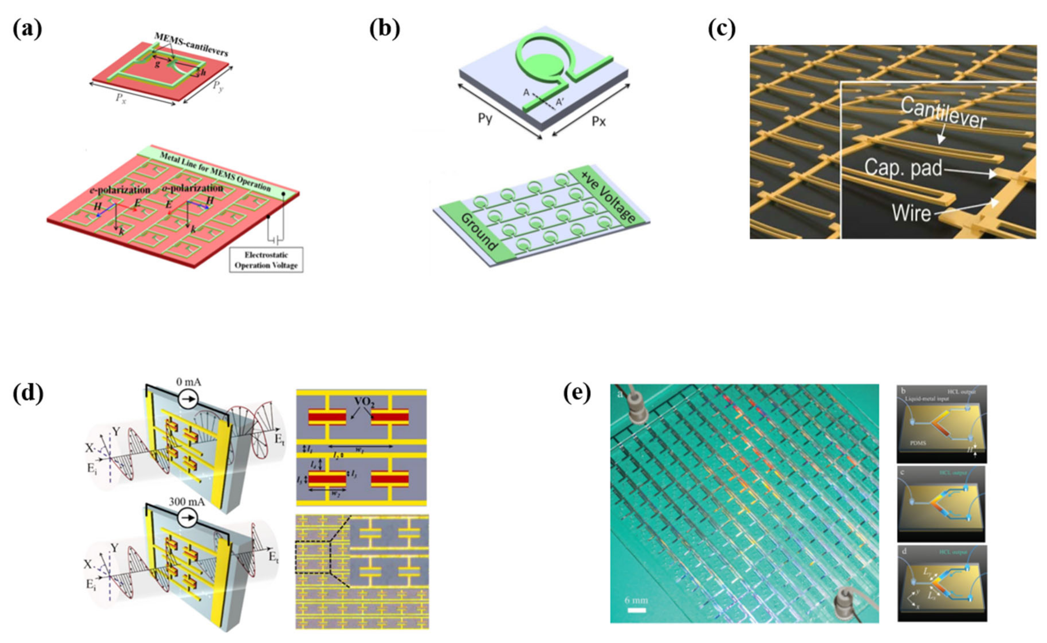
- Zheludev, N.I.; Plum, E. Reconfigurable nanomechanical photonic metamaterials. Nat. Nanotechnol. 2016, 11, 16–22. [Google Scholar] [CrossRef] [Green Version]
- Ho, C.P.; Pitchappa, P.; Lin, Y.S.; Huang, C.Y.; Kropelnicki, P.; Lee, C. Electrothermally actuated microelectromechanical systems based omega-ring terahertz metamaterial with polarization dependent characteristics. Appl. Phys. Lett. 2014, 104. [Google Scholar] [CrossRef] [Green Version]
- Zhao, X.; Schalch, J.; Zhang, J.; Seren, H.R.; Duan, G.; Averitt, R.D.; Zhang, X. Electromechanically tunable metasurface transmission waveplate at terahertz frequencies. Optica 2018, 5, 303. [Google Scholar] [CrossRef]
- Wu, P.C.; Zhu, W.; Shen, Z.X.; Chong, P.H.J.; Ser, W.; Tsai, D.P.; Liu, A.Q. Broadband Wide-Angle Multifunctional Polarization Converter via Liquid-Metal-Based Metasurface. Adv. Opt. Mater. 2017, 5, 1–7. [Google Scholar] [CrossRef]
- Ma, F.; Qian, Y.; Lin, Y.S.; Liu, H.; Zhang, X.; Liu, Z.; Ming-Lin Tsai, J.; Lee, C. Polarization-sensitive microelectromechanical systems based tunable terahertz metamaterials using three dimensional electric split-ring resonator arrays. Appl. Phys. Lett. 2013, 102. [Google Scholar] [CrossRef]
- Nouman, M.T.; Hwang, J.H.; Faiyaz, M.; Lee, K.-J.; Noh, D.-Y.; Jang, J.-H. Vanadium dioxide based frequency tunable metasurface filters for realizing reconfigurable terahertz optical phase and polarization control. Opt. Express 2018, 26, 12922. [Google Scholar] [CrossRef] [PubMed]
- Sugano, S.; Kojima, N. Magneto-Optics; Springer: Berlin/Heidelberg, Germany, 2000; ISBN 9783662041437. [Google Scholar]
- Misemer, D.K. The effect of spin-orbit interaction and exchange splitting on magneto-optic coefficients. J. Magn. Magn. Mater. 1988, 72, 267–274. [Google Scholar] [CrossRef]
- Stupakiewicz, A.; Chizhik, A.; Tekielak, M.; Zhukov, A.; Gonzalez, J.; Maziewski, A. Direct imaging of the magnetization reversal in microwires using all-MOKE microscopy. Rev. Sci. Instrum. 2014, 85, 103702. [Google Scholar] [CrossRef]
- McDaniel, T. Magneto-optical data storage. Commun. ACM 2000, 43, 56–63. [Google Scholar] [CrossRef]
- Shoji, Y.; Mizumoto, T.; Yokoi, H.; Hsieh, I.-W.; Osgood, R.M. Magneto-optical isolator with silicon waveguides fabricated by direct bonding. Appl. Phys. Lett. 2008, 92, 071117. [Google Scholar] [CrossRef]
- Tien, P.K.; Martin, R.J.; Wolfe, R.; Le Craw, R.C.; Blank, S.L. Switching and modulation of light in magneto-optic waveguides of garnet films. Appl. Phys. Lett. 1972, 21, 394–396. [Google Scholar] [CrossRef]
- Kim, S.; Hong, Y.-P.; Kim, Y.-G.; Lee, D.-J. Field-calibrated magneto-optic sensor based on off-axis optical probing of intense magnetic fields. Appl. Opt. 2017, 56, 1701. [Google Scholar] [CrossRef]
- Chiu, K.W.; Quinn, J.J. Magnetoplasma Surface Waves in Metals. Phys. Rev. B 1972, 5, 4707–4709. [Google Scholar] [CrossRef]
- Floess, D.; Giessen, H. Nonreciprocal hybrid magnetoplasmonics. Rep. Prog. Phys. 2018, 81, 116401. [Google Scholar] [CrossRef] [PubMed] [Green Version]
- Chen, J.; Albella, P.; Pirzadeh, Z.; Alonso-González, P.; Huth, F.; Bonetti, S.; Bonanni, V.; Åkerman, J.; Nogués, J.; Vavassori, P.; et al. Plasmonic Nickel Nanoantennas. Small 2011, 7, 2341–2347. [Google Scholar] [CrossRef] [PubMed] [Green Version]
- Tomitaka, A.; Arami, H.; Raymond, A.; Yndart, A.; Kaushik, A.; Jayant, R.D.; Takemura, Y.; Cai, Y.; Toborek, M.; Nair, M. Development of magneto-plasmonic nanoparticles for multimodal image-guided therapy to the brain. Nanoscale 2017, 9, 764–773. [Google Scholar] [CrossRef] [Green Version]
- Urries, I.; Muñoz, C.; Gomez, L.; Marquina, C.; Sebastian, V.; Arruebo, M.; Santamaria, J. Magneto-plasmonic nanoparticles as theranostic platforms for magnetic resonance imaging, drug delivery and NIR hyperthermia applications. Nanoscale 2014, 6, 9230. [Google Scholar] [CrossRef] [Green Version]
- Pineider, F.; Sangregorio, C. Nanomaterials for Magnetoplasmonics ☆. In Novel Magnetic Nanostructures; Elsevier: Amsterdam, The Netherlands, 2018; pp. 191–220. [Google Scholar]
- Li, Y.; Zhang, Q.; Nurmikko, A.V.; Sun, S. Enhanced Magnetooptical Response in Dumbbell-like Ag−CoFe 2 O 4 Nanoparticle Pairs. Nano Lett. 2005, 5, 1689–1692. [Google Scholar] [CrossRef]
- Jain, P.K.; Xiao, Y.; Walsworth, R.; Cohen, A.E. Surface Plasmon Resonance Enhanced Magneto-Optics (SuPREMO): Faraday Rotation Enhancement in Gold-Coated Iron Oxide Nanocrystals. Nano Lett. 2009, 9, 1644–1650. [Google Scholar] [CrossRef]
- Wang, L.; Clavero, C.; Huba, Z.; Carroll, K.J.; Carpenter, E.E.; Gu, D.; Lukaszew, R.A. Plasmonics and Enhanced Magneto-Optics in Core-Shell Co-Ag Nanoparticles. Nano Lett. 2011, 11, 37. [Google Scholar] [CrossRef] [Green Version]
- Chin, J.Y.; Steinle, T.; Wehlus, T.; Dregely, D.; Weiss, T.; Belotelov, V.I.; Stritzker, B.; Giessen, H. Nonreciprocal plasmonics enables giant enhancement of thin-film Faraday rotation. Nat. Commun. 2013, 4, 1599. [Google Scholar] [CrossRef] [Green Version]
- Fujikawa, R.; Baryshev, A.V.; Kim, J.; Uchida, H.; Inoue, M. Contribution of the surface plasmon resonance to optical and magneto-optical properties of a Bi:YIG-Au nanostructure. J. Appl. Phys. 2008, 103, 07D301. [Google Scholar] [CrossRef]
- Floess, D.; Chin, J.Y.; Kawatani, A.; Dregely, D.; Habermeier, H.-U.; Weiss, T.; Giessen, H. Tunable and switchable polarisation rotation with non-reciprocal plasmonic thin films at designated wavelengths. Light Sci. Appl. 2015, 4, e284. [Google Scholar] [CrossRef] [Green Version]
- Kuzmichev, A.N.; Sylgacheva, D.A.; Kozhaev, M.A.; Krichevsky, D.M.; Shaposhnikov, A.N.; Berzhansky, V.N.; Freire-Fernández, F.; Qin, H.J.; Popova, O.E.; Keller, N.; et al. Influence of the Plasmonic Nanodisk Positions Inside a Magnetic Medium on the Faraday Effect Enhancement. Phys. Status Solidi Rapid Res. Lett. 2020, 14, 1–4. [Google Scholar] [CrossRef]
- Crassee, I.; Levallois, J.; Walter, A.L.; Ostler, M.; Bostwick, A.; Rotenberg, E.; Seyller, T.; van der Marel, D.; Kuzmenko, A.B. Giant Faraday rotation in single- and multilayer graphene. Nat. Phys. 2011, 7, 48–51. [Google Scholar] [CrossRef] [Green Version]
- Tymchenko, M.; Nikitin, A.Y.; Martín-Moreno, L. Faraday Rotation Due to Excitation of Magnetoplasmons in Graphene Microribbons. ACS Nano 2013, 7, 9780–9787. [Google Scholar] [CrossRef] [Green Version]
- Kimel, A.V.; Kirilyuk, A.; Usachev, P.A.; Pisarev, R.V.; Balbashov, A.M.; Rasing, T. Ultrafast non-thermal control of magnetization by instantaneous photomagnetic pulses. Nature 2005, 435, 655–657. [Google Scholar] [CrossRef]
- Kruglyak, V.V.; Hicken, R.J.; Ali, M.; Hickey, B.J.; Pym, A.T.G.; Tanner, B.K. Ultrafast third-order optical nonlinearity of noble and transition metal thin films. J. Opt. A Pure Appl. Opt. 2005, 7. [Google Scholar] [CrossRef]
- Hansteen, F.; Kimel, A.; Kirilyuk, A.; Rasing, T. Nonthermal ultrafast optical control of the magnetization in garnet films. Phys. Rev. B–Condens. Matter Mater. Phys. 2006, 73, 014421. [Google Scholar] [CrossRef] [Green Version]
- Cheng, O.H.-C.; Son, D.H.; Sheldon, M. Light-induced magnetism in plasmonic gold nanoparticles. Nat. Photonics 2020, 1–4. [Google Scholar] [CrossRef] [Green Version]
- Bonanni, V.; Bonetti, S.; Pakizeh, T.; Pirzadeh, Z.; Chen, J.; Nogués, J.; Vavassori, P.; Hillenbrand, R.; Åkerman, J.; Dmitriev, A. Designer Magnetoplasmonics with Nickel Nanoferromagnets. Nano Lett. 2011, 11, 5333–5338. [Google Scholar] [CrossRef]
- Safarov, V.I.; Kosobukin, V.A.; Hermann, C.; Lampel, G.; Peretti, J.; Marlière, C. Magneto-optical effects enhanced by surface plasmons in metallic multilayer films. Phys. Rev. Lett. 1994, 73, 3584–3587. [Google Scholar] [CrossRef]
- González-Díaz, J.B.; García-Martín, A.; García-Martín, J.M.; Cebollada, A.; Armelles, G.; Sepúlveda, B.; Alaverdyan, Y.; Käll, M. Plasmonic Au/Co/Au Nanosandwiches with Enhanced Magneto-optical Activity. Small 2008, 4, 202–205. [Google Scholar] [CrossRef] [PubMed]
- López-Ortega, A.; Zapata-Herrera, M.; Maccaferri, N.; Pancaldi, M.; Garcia, M.; Chuvilin, A.; Vavassori, P. Enhanced magnetic modulation of light polarisation exploiting hybridization with multipolar dark plasmons in magnetoplasmonic nanocavities. Light Sci. Appl. 2020, 9. [Google Scholar] [CrossRef] [PubMed] [Green Version]
- Kreilkamp, L.E.; Belotelov, V.I.; Chin, J.Y.; Neutzner, S.; Dregely, D.; Wehlus, T.; Akimov, I.A.; Bayer, M.; Stritzker, B.; Giessen, H. Waveguide-Plasmon Polaritons Enhance Transverse Magneto-Optical Kerr Effect. Phys. Rev. X 2013, 3, 041019. [Google Scholar] [CrossRef] [Green Version]
- Manera, M.G.; Colombelli, A.; Taurino, A.; Martin, A.G.; Rella, R. Magneto-Optical properties of noble-metal nanostructures: Functional nanomaterials for bio sensing. Sci. Rep. 2018, 8, 12640. [Google Scholar] [CrossRef] [PubMed] [Green Version]
- Rizal, C.; Kapralov, P.O.; Ignatyeva, D.; Belotelov, V.; Pisana, S. Comparison of the effects of surface plasmon resonance and the transverse magneto-optic Kerr effect in magneto-optic plasmonic nanostructures. J. Phys. D Appl. Phys. 2020, 53, 02LT02. [Google Scholar] [CrossRef]
- Pendry, J.B.; Holden, A.J.; Robbins, D.J.; Stewart, W.J. Magnetism from conductors and enhanced nonlinear phenomena. IEEE Trans. Microw. Theory Tech. 1999, 47, 2075–2084. [Google Scholar] [CrossRef] [Green Version]
- Klein, M.W.; Enkrich, C.; Wegener, M.; Soukoulis, C.M.; Linden, S. Single-slit split-ring resonators at optical frequencies: Limits of size scaling. Opt. Lett. 2006, 31, 1259–1261. [Google Scholar] [CrossRef] [Green Version]
- Bao, Y.; Hu, Z.; Li, Z.; Zhu, X.; Fang, Z. Magnetic Plasmonic Fano Resonance at Optical Frequency. Small 2015, 11, 2177–2181. [Google Scholar] [CrossRef]
- Kuznetsov, A.I.; Miroshnichenko, A.E.; Hsing Fu, Y.; Viswanathan, V.; Rahmani, M.; Valuckas, V.; Ying Pan, Z.; Kivshar, Y.; Pickard, D.S.; Luk’Yanchuk, B. Split-ball resonator as a three-dimensional analogue of planar split-rings. Nat. Commun. 2014, 5, 1–8. [Google Scholar] [CrossRef] [Green Version]
- Wang, P.; Huh, J.; Lee, J.; Kim, K.; Park, K.J.; Lee, S.; Ke, Y. Magnetic Plasmon Networks Programmed by Molecular Self-Assembly. Adv. Mater. 2019, 31, 1901364. [Google Scholar] [CrossRef]
- Monticone, F.; Alù, A. The quest for optical magnetism: From split-ring resonators to plasmonic nanoparticles and nanoclusters. J. Mater. Chem. C 2014, 2, 9059–9072. [Google Scholar] [CrossRef]
- Calandrini, E.; Cerea, A.; De Angelis, F.; Zaccaria, R.P.; Toma, A. Magnetic hot-spot generation at optical frequencies: From plasmonic metamolecules to all-dielectric nanoclusters. Nanophotonics 2018, 8, 45–62. [Google Scholar] [CrossRef]
- Sandrock, M.L.; Pibel, C.D.; Geiger, F.M.; Foss, C.A. Synthesis and second-harmonic generation studies of noncentrosymmetric gold nanostructures. J. Phys. Chem. B 1999, 103, 2668–2673. [Google Scholar] [CrossRef]
- Lippitz, M.; Van Dijk, M.A.; Orrit, M. Third-harmonic generation from single gold nanoparticles. Nano Lett. 2005, 5, 799–802. [Google Scholar] [CrossRef]
- Kruk, S.; Weismann, M.; Bykov, A.Y.; Mamonov, E.A.; Kolmychek, I.A.; Murzina, T.; Panoiu, N.C.; Neshev, D.N.; Kivshar, Y.S. Enhanced Magnetic Second-Harmonic Generation from Resonant Metasurfaces. ACS Photonics 2015, 2, 1007–1012. [Google Scholar] [CrossRef] [Green Version]
- Ding, S.J.; Zhang, H.; Yang, D.J.; Qiu, Y.H.; Nan, F.; Yang, Z.J.; Wang, J.; Wang, Q.Q.; Lin, H.Q. Magnetic Plasmon-Enhanced Second-Harmonic Generation on Colloidal Gold Nanocups. Nano Lett. 2019, 19, 2005–2011. [Google Scholar] [CrossRef]
- Shcherbakov, M.R.; Neshev, D.N.; Hopkins, B.; Shorokhov, A.S.; Staude, I.; Melik-Gaykazyan, E.V.; Decker, M.; Ezhov, A.A.; Miroshnichenko, A.E.; Brener, I.; et al. Enhanced third-harmonic generation in silicon nanoparticles driven by magnetic response. Nano Lett. 2014, 14, 6488–6492. [Google Scholar] [CrossRef]
- Krutyanskiy, V.L.; Kolmychek, I.A.; Gan’shina, E.A.; Murzina, T.V.; Evans, P.; Pollard, R.; Stashkevich, A.A.; Wurtz, G.A.; Zayats, A.V. Plasmonic enhancement of nonlinear magneto-optical response in nickel nanorod metamaterials. Phys. Rev. B 2013, 87, 035116. [Google Scholar] [CrossRef] [Green Version]
- Kolmychek, I.A.; Shaimanov, A.N.; Baryshev, A.V.; Murzina, T. V Magnetization-induced effects in second harmonic generation under the lattice plasmon resonance excitation. Opt. Lett. 2016, 41, 5446. [Google Scholar] [CrossRef]
- Valev, V.K.; Silhanek, A.V.; Gillijns, W.; Jeyaram, Y.; Paddubrouskaya, H.; Volodin, A.; Biris, C.G.; Panoiu, N.C.; De Clercq, B.; Ameloot, M.; et al. Plasmons reveal the direction of magnetization in nickel nanostructures. ACS Nano 2011, 5, 91–96. [Google Scholar] [CrossRef] [Green Version]
- Pineider, F.; Campo, G.; Bonanni, V.; Fernández, C.D.J.; Mattei, G.; Caneschi, A.; Gatteschi, D.; Sangregorio, C. Circular magnetoplasmonic modes in gold nanoparticles. Nano Lett. 2013, 13, 4785–4789. [Google Scholar] [CrossRef] [PubMed]
- Melnikau, D.; Govyadinov, A.A.; Sánchez-Iglesias, A.; Grzelczak, M.; Liz-Marzán, L.M.; Rakovich, Y.P. Strong Magneto-Optical Response of Nonmagnetic Organic Materials Coupled to Plasmonic Nanostructures. Nano Lett. 2017, 17, 1808–1813. [Google Scholar] [CrossRef]
- Shiratsu, T.; Yao, H. Magnetic circular dichroism (MCD) in silver nanocubes with different sizes. Chem. Phys. Lett. 2018, 706, 607–612. [Google Scholar] [CrossRef]
- Yin, P.; Tan, Y.; Fang, H.; Hegde, M.; Radovanovic, P.V. Plasmon-induced carrier polarisation in semiconductor nanocrystals. Nat. Nanotechnol. 2018, 13, 463–467. [Google Scholar] [CrossRef] [PubMed]
- Pineider, F.; de Julián Fernández, C.; Videtta, V.; Carlino, E.; al Hourani, A.; Wilhelm, F.; Rogalev, A.; Cozzoli, P.D.; Ghigna, P.; Sangregorio, C. Spin-Polarisation Transfer in Colloidal Magnetic-Plasmonic Au/Iron Oxide Hetero-nanocrystals. ACS Nano 2013, 7, 857–866. [Google Scholar] [CrossRef]
- Sepúlveda, B.; Calle, A.; Lechuga, L.M.; Armelles, G. Highly sensitive detection of biomolecules with the magneto-optic surface-plasmon-resonance sensor. Opt. Lett. 2006, 31, 1085. [Google Scholar] [CrossRef] [PubMed]
- Rizal, C.; Pisana, S.; Hrvoic, I.; Fullerton, E.E. Microstructure and magneto-optical surface plasmon resonance of Co/Au multilayers. J. Phys. Commun. 2018, 2, 055010. [Google Scholar] [CrossRef]
- Manera, M.G.; Colombelli, A.; Rella, R.; Caricato, A.; Cozzoli, P.D.; Martino, M.; Vasanelli, L. TiO 2 brookite nanostructured thin layer on magneto-optical surface plasmon resonance transductor for gas sensing applications. J. Appl. Phys. 2012, 112, 053524. [Google Scholar] [CrossRef]
- Zubritskaya, I.; Lodewijks, K.; Maccaferri, N.; Mekonnen, A.; Dumas, R.K.; Åkerman, J.; Vavassori, P.; Dmitriev, A. Active Magnetoplasmonic Ruler. Nano Lett. 2015, 15, 3204–3211. [Google Scholar] [CrossRef] [PubMed] [Green Version]
- Wang, X.; Feng, J.; Yu, H.; Jin, Y.; Davidson, A.; Li, Z.; Yin, Y. Anisotropically Shaped Magnetic/Plasmonic Nanocomposites for Information Encryption and Magnetic-Field-Direction Sensing. Research 2018, 2018, 1–13. [Google Scholar] [CrossRef] [Green Version]
- Pancaldi, M.; Leo, N.; Vavassori, P. Selective and fast plasmon-assisted photo-heating of nanomagnets. Nanoscale 2019, 11, 7656–7666. [Google Scholar] [CrossRef] [PubMed]
- Belotelov, V.I.; Kreilkamp, L.E.; Akimov, I.A.; Kalish, A.N.; Bykov, D.A.; Kasture, S.; Yallapragada, V.J.; Gopal, A.V.; Grishin, A.M.; Khartsev, S.I.; et al. Plasmon-mediated magneto-optical transparency. Nat. Commun. 2013, 4, 1–7. [Google Scholar] [CrossRef] [PubMed] [Green Version]
- Zubritskaya, I.; Maccaferri, N.; Inchausti Ezeiza, X.; Vavassori, P.; Dmitriev, A. Magnetic Control of the Chiroptical Plasmonic Surfaces. Nano Lett. 2018, 18, 302–307. [Google Scholar] [CrossRef] [PubMed]
- Song, Y.; Tran, V.T.; Lee, J. Tuning Plasmon Resonance in Magnetoplasmonic Nanochains by Controlling Polarisation and Interparticle Distance for Simple Preparation of Optical Filters. ACS Appl. Mater. Interfaces 2017, 9, 24433–24439. [Google Scholar] [CrossRef]


| Material | Mechanism | Possible Application | References |
|---|---|---|---|
| Plasmonic nanowire on magnetic film | Faraday effect | Tunable and switchable polarisation rotation for optical isolators | [202,204] |
| Gold nanoparticles in solution | Inverse Faraday effect | Optical isolation without external magnetic fields | [211] |
| Plasmonic—magnetic film | Kerr effect | Magneto-optical surface plasmon resonance | [218,239] |
| Nickel nanodiscs | Kerr effect | Active ruler utilising polarisation, monitoring polarisation-selective photo-heating | [242,244] |
| Plasmonic resonator structures | Magnetic plasmon resonance | Surface-enhanced Raman scattering, nanoantennas | [221,222] |
| G-shaped nickel nanostructures | Magnetic second-harmonic generation | Probing the magnetisation direction | [233] |
| Plasmonic nanoparticles | Magnetic circular dichroism | Sensing by monitoring the intensity of circularly polarised light | [235] |
| Assembled chains of magnetic-plasmonic nanoparticles | Dipole–dipole magnetic interaction | Optical filtering | [247] |
© 2020 by the authors. Licensee MDPI, Basel, Switzerland. This article is an open access article distributed under the terms and conditions of the Creative Commons Attribution (CC BY) license (http://creativecommons.org/licenses/by/4.0/).
Share and Cite
Khan, P.; Brennan, G.; Lillis, J.; Tofail, S.A.M.; Liu, N.; Silien, C. Characterisation and Manipulation of Polarisation Response in Plasmonic and Magneto-Plasmonic Nanostructures and Metamaterials. Symmetry 2020, 12, 1365. https://doi.org/10.3390/sym12081365
Khan P, Brennan G, Lillis J, Tofail SAM, Liu N, Silien C. Characterisation and Manipulation of Polarisation Response in Plasmonic and Magneto-Plasmonic Nanostructures and Metamaterials. Symmetry. 2020; 12(8):1365. https://doi.org/10.3390/sym12081365
Chicago/Turabian StyleKhan, Pritam, Grace Brennan, James Lillis, Syed A. M. Tofail, Ning Liu, and Christophe Silien. 2020. "Characterisation and Manipulation of Polarisation Response in Plasmonic and Magneto-Plasmonic Nanostructures and Metamaterials" Symmetry 12, no. 8: 1365. https://doi.org/10.3390/sym12081365