1. Introduction
Periodic structures made with metallic pins have been used by the electromagnetism community in different kinds of applications. The original structure known as “the bed of nails” [
1] can be considered a metasurface and is able to provide extraordinary boundary conditions. This property was used in the definition of a new technology known as a gap waveguide [
2,
3], where the structure is combined with a top metal lid to provide the cutoff frequency or stopband for all the parallel plate modes [
4]. In this case, the pin structure acts as an artificial magnetic conductor (AMC) within a given frequency range, producing a stopband. This same concept was also used as a successful packaging solution [
5] using not only pins but also other versions of symmetrical and periodic “pin-like” structures [
6,
7,
8]. A similar idea was also implemented using dielectric materials [
9] rather than metal.
Gap waveguide technology is currently a reality and its use in designing antennas and components has been widely extended [
10]. Alternatives to pin structures to create the stopband in a PPWG have emerged, such as half-size pins [
11] and holes [
12,
13], mainly with the purpose of providing easier manufacturing of this technology.
On the other hand, these pin structures have been also used to create effective refractive indices without using dielectrics. This property was used to design lenses [
14] or even prisms to compensate the dispersion of a conventional leaky wave antenna [
15]. For this type of application, the structure of the pins is well located within the parallel plate structure and modifies the dispersion characteristics of the first propagating mode.
Recently, higher symmetries have been proposed for periodic structures in the form of corrugations [
13,
16] to obtain either less dispersive behavior of the propagating mode for designing lenses [
17] or to increase the stopbands for use in gap waveguide technology. Other similar periodic structures have been studied and applied in the optical domain [
18,
19].
The purpose of this work is to present a complete analysis of pin structures inside a parallel plate waveguide in terms of stopbands, equivalent refractive index and dispersion of the first propagating mode. In the study, we focus on the analysis of innovative configurations of pins in terms of a combination of pins with different characteristics or the use of higher symmetries such as glide symmetry.
2. Geometries Considered in the Analysis
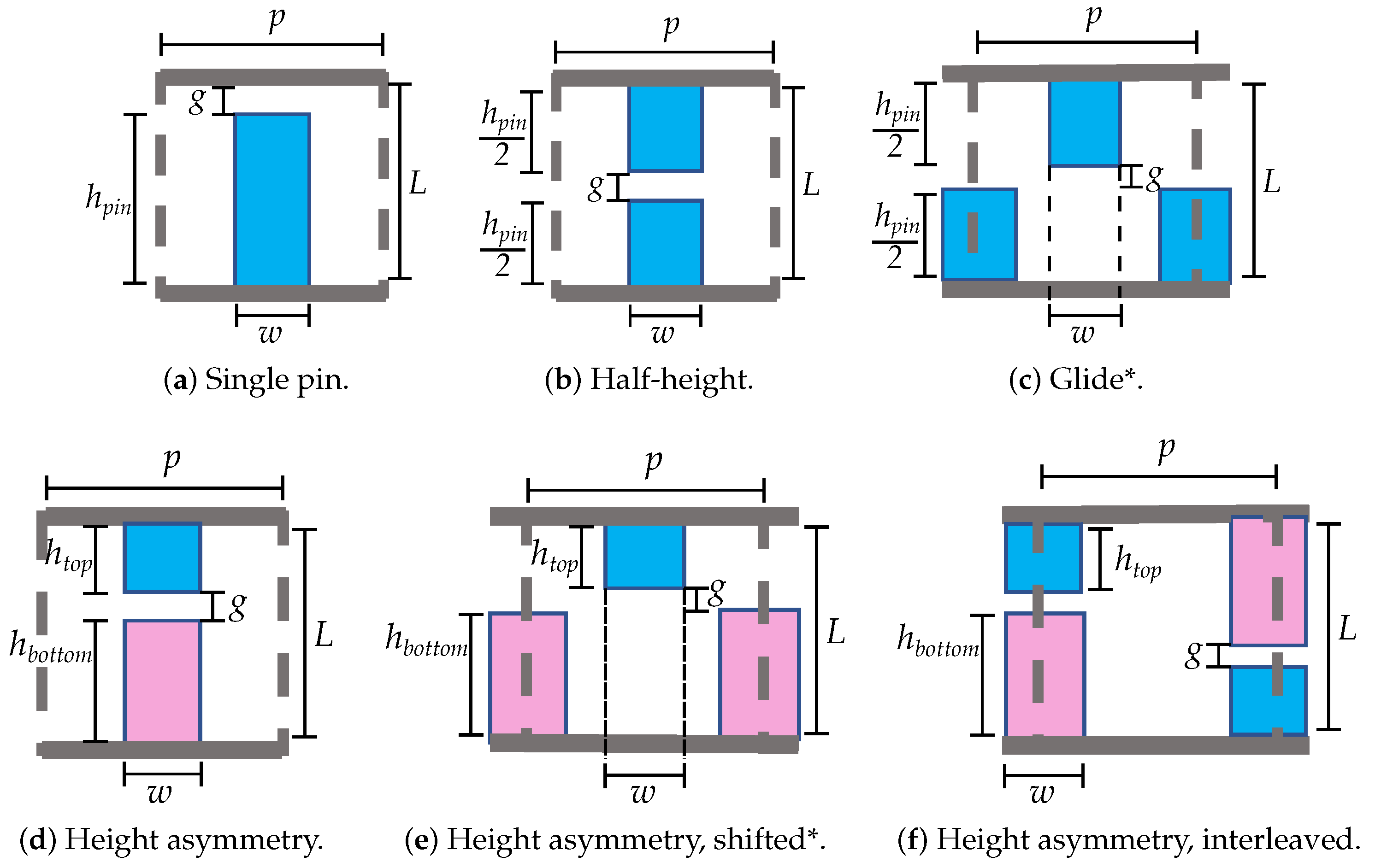
The pin structures that are considered in this study are presented in
Figure 1.
In our work, the reference case is the conventional pin (
Figure 1a), where
is the height of the pin,
w is the width of the pin,
L is the distance between the two plates and
g is the gap either between the top plate and the pin or between the top and bottom pins. A second case of the study is a symmetric double pin with half of the height of the reference pin (
) as shown in
Figure 2b. This geometry has been extensively studied in the paper [
11] in terms of its stopband properties. We will also include here the propagation properties, i.e., the dispersion of the first mode. A third case is the glide symmetric case (
Figure 2c), i.e., a translation in the longitudinal direction of
and a reflection with respect to the
plane. Here, we consider the cases of only the half-pin translation in one direction (generically named as
X) and the shift in two directions (named as
).
Three other structures are proposed in this study and are described in
Figure 1d–f. The key difference of these structures is that they present asymmetries related to the previous ones already introduced. In particular, we will study the effect of using unequal pins in the top (with height
) and bottom (with height
) of the metal plate and also interleaving these different pins. Finally,
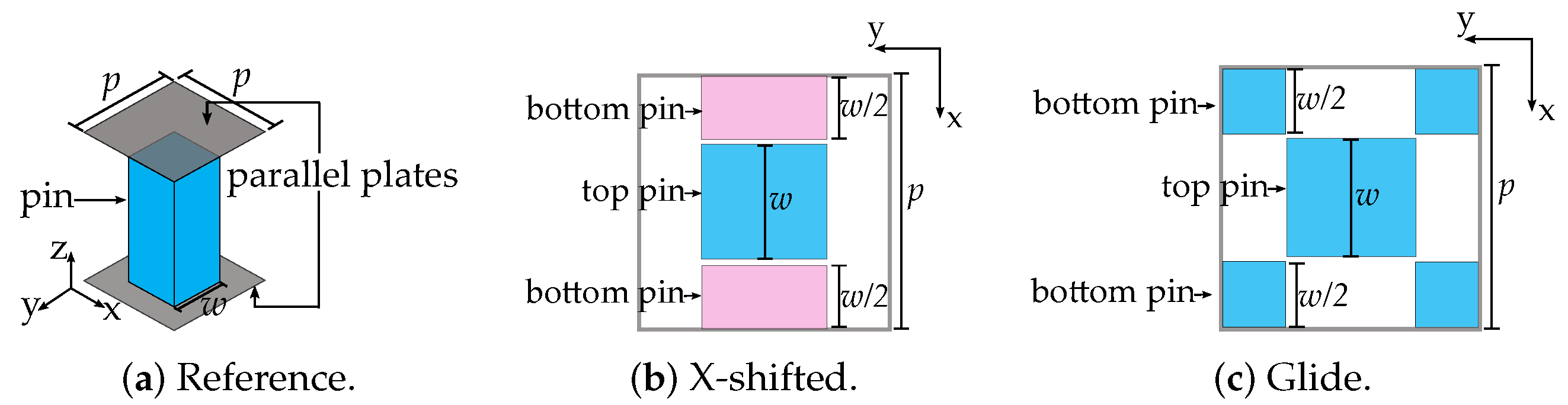
Figure 2 contains additional representations of the cases under study including the reference coordinate axes.
In order to compare the six structures, some key parameters will be fixed for all the cases. The distance
L between the two plates, the gap size
g, the pin width
w and the periodicity
p will remain constant in this initial study. The effect of all these parameters has been extensively analyzed in [
4] for the reference case. In the second part of this work, we also include a parametric study for all the other proposed geometries.
3. Stopband Analysis
Simulations of the parallel plate stopband were carried out by calculating the dispersion diagram of a unit cell using the commercial software CST Microwave Studio. Alternative methodologies for calculating dispersion diagrams of these kinds of structures were presented in [
20].
As for the pin structure, we have selected the following dimensions: mm, mm, mm and mm. However, we have decided to normalize all the frequencies to the frequency where the pin height for the reference case is 0.25. As a consequence and without loss of generality, with the selected of 2.5 mm, corresponds to 30 GHz.
The selection of some initial dimensions and their normalization with respect to a frequency is a common practice when doing parametric studies(see the previous examples in [
4,
11,
12]). It is important to mention that as a consequence of the linearity of the electromagnetism, the results can be directly scaled to any desired frequency range.
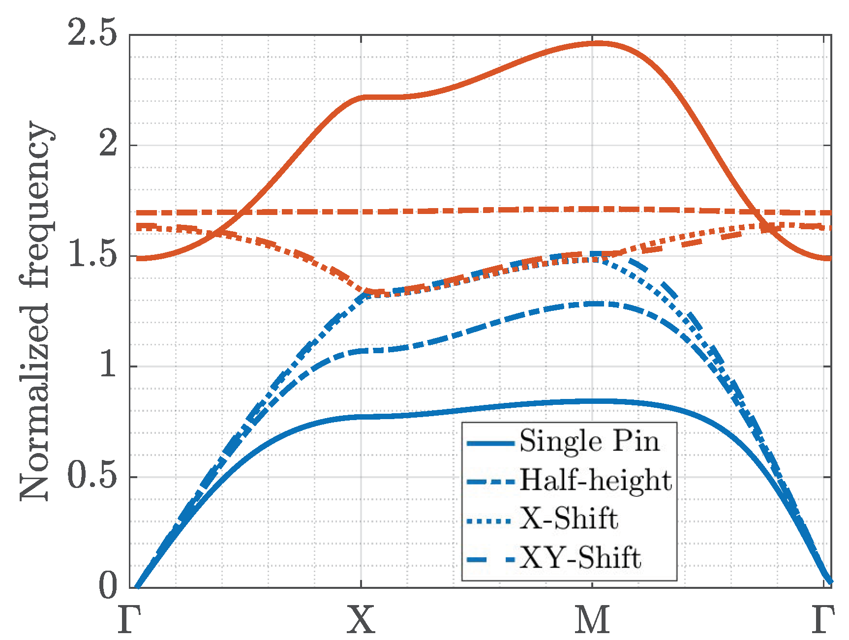
First, the calculated dispersion diagrams of the first two modes for the reference pin (
Figure 1a), the double pin (
Figure 2b) and glide symmetry cases with a shift in one direction and two directions (
Figure 2c) are presented in
Figure 3. In this figure the blue curves correspond to the dispersion diagram of the first mode of the geometry while the red curves correspond to the second propagating mode of the geometry. We can observe that reference (case
a) has the largest stopband. The case named half-height (case
b) has a higher cutoff frequency of the first mode, and the second mode is flat in frequency, meaning that it cannot be used to propagate energy and corresponds to a resonance. Finally, in the glide case, when we shift the pins (case
c) in the bottom layer by half the period with respect to the pins in the top layer (in one or two directions), the stopband disappears between the first and second modes, as previously observed for glide corrugations [
16]. Note that in this case there is a very narrow stopband between the second and third modes.
Concerning the analysis of the asymmetrical cases from
Figure 1, we start with case
d (
Figure 1d). In
Figure 4, the variation in the dispersion diagram for the double-pin structure when the pins in the top and bottom plates have different heights (
and
, respectively) is represented. For this analysis, we always consider that the total height (
) is equal to the height of the reference pin
mm. The consequence of increasing the height of one of the pins is a reduction in the cutoff frequency of the first and second modes.
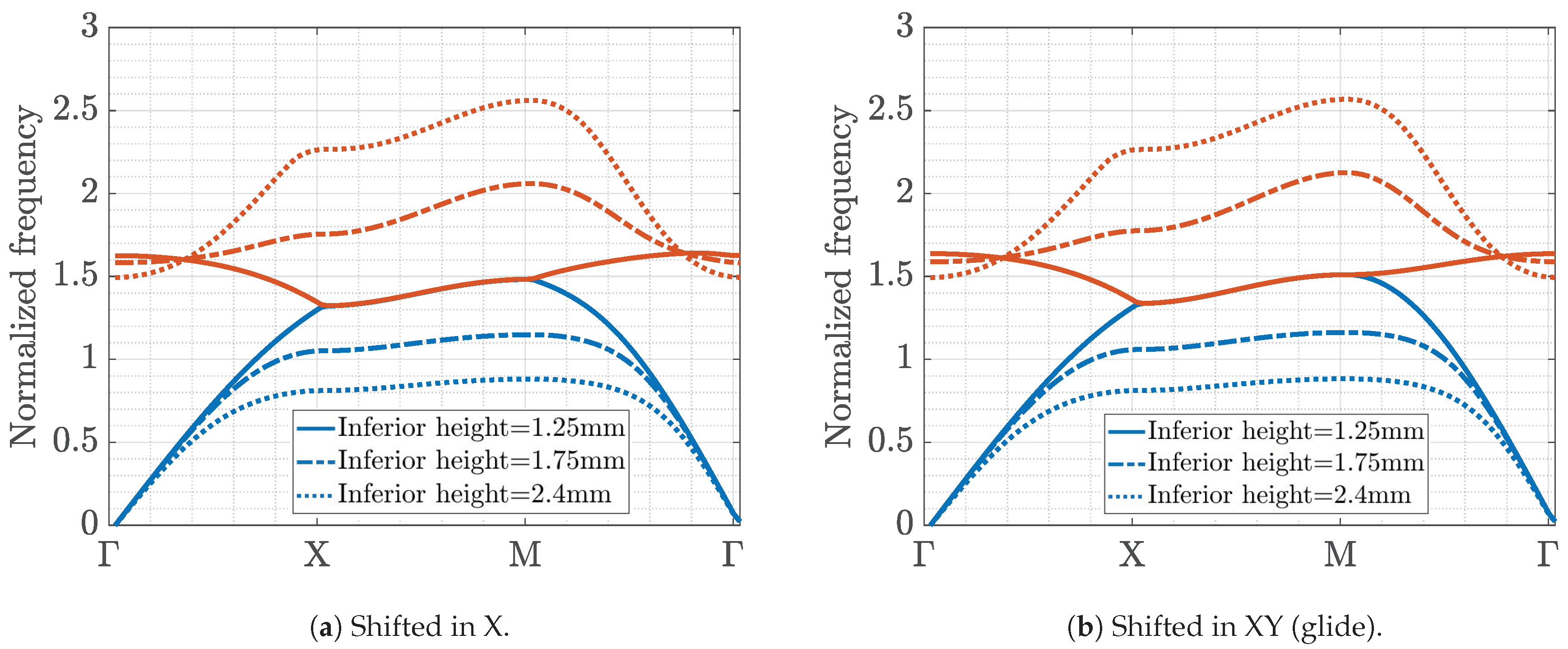
The next step was to analyze the effect of shifting the asymmetrical pins (case
e) as described in
Figure 1e. An example of this study is presented in
Figure 5. First, we considered a shift in one direction (
Figure 5a) and then a shift in XY (
Figure 5b). It can be seen that the effects in both cases are similar. Only when the two pins (top and bottom) had identical heights, the stopband between the first two modes disappeared. When the pins had different heights, the stopband existed.
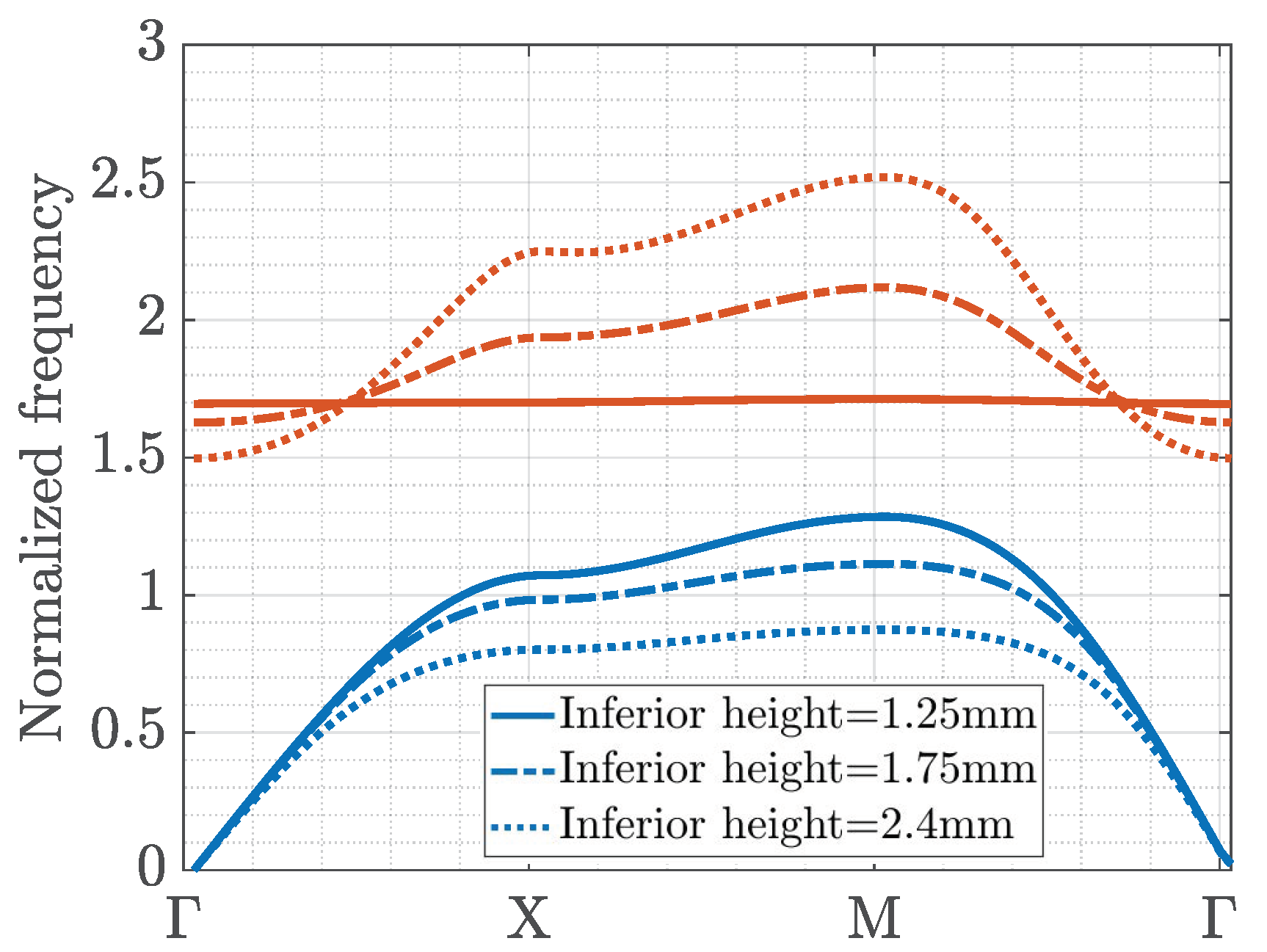
The last case to be analyzed was the interleaving of pins with different heights in the top and bottom layers (case
f) as shown in
Figure 1f. In this particular case, we needed to use a unit cell with a doubled size to ensure the right symmetry when applying periodic boundary conditions. The results for two different interleaved heights (
mm and
mm) are shown in
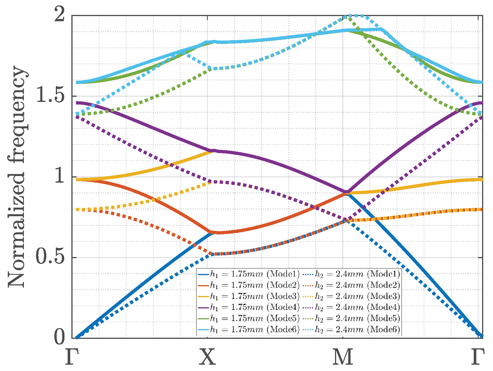
Figure 6. In this case, a narrow stopband occurs only for very-high-order modes. We can conclude for this case that the high number of modes is just a consequence of the supersymmetry of the unit cell. Moreover, we can easily see how there is continuity among the first five modes, which in practice is just a single mode. Additionally, note that the stopband is in the same frequency range as that for the previously studied geometries.
Finally, a summary of the obtained stopbands for the different structures is represented in
Table 1, with
corresponding to the normalized starting frequency of the stopband and
being the normalized end frequency of the stopband. The cases with glide symmetry (case
c) are not included as the stopband is practically nonexistent. The case of interleaved pins refers to the bandgap between high-order modes; nonetheless, this stopband exists in the same frequency range as that for the other geometries.
From this first comparative analysis among the different proposed geometries, several conclusions are derived. When dealing with shifted geometries (X or XY), the use of unequal pins in the top and bottom plates preserved the stopbands, whilst the use of identical pins made it disappear. On the other hand, when these unequal pins were interleaved, again there was no stopband.
Parametric Study for Cases with Pins of Unequal Heights
In this section, we include a brief parametric study of some of the geometries. The type of representation is similar to the ones presented in [
4,
11]. The complete study of all the cases in most situations gives the same type of conclusions as in the previous studies, and for this reason we have selected some representative cases to be shown here. The range of variation of the different parameters has been also taken from these previous studies as the intention of the present work is to analyze the effect of the specific geometry.
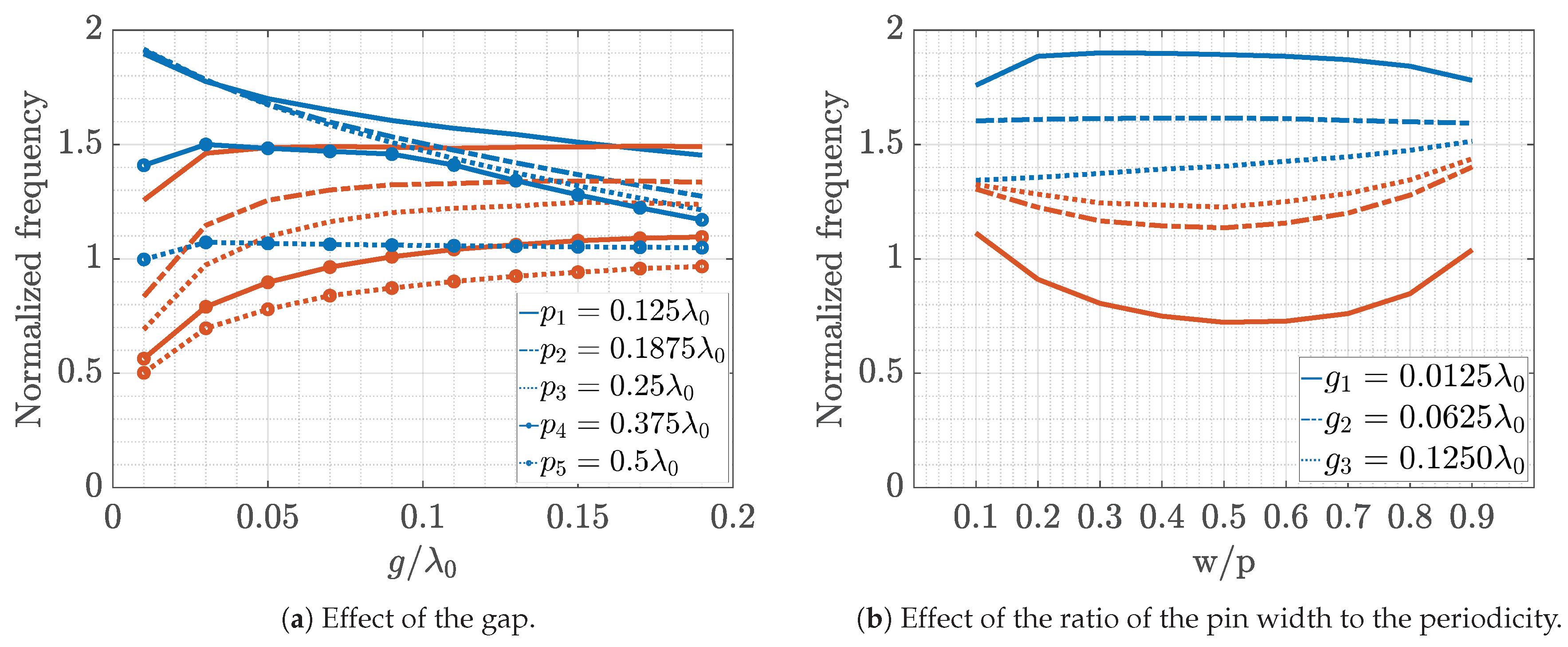
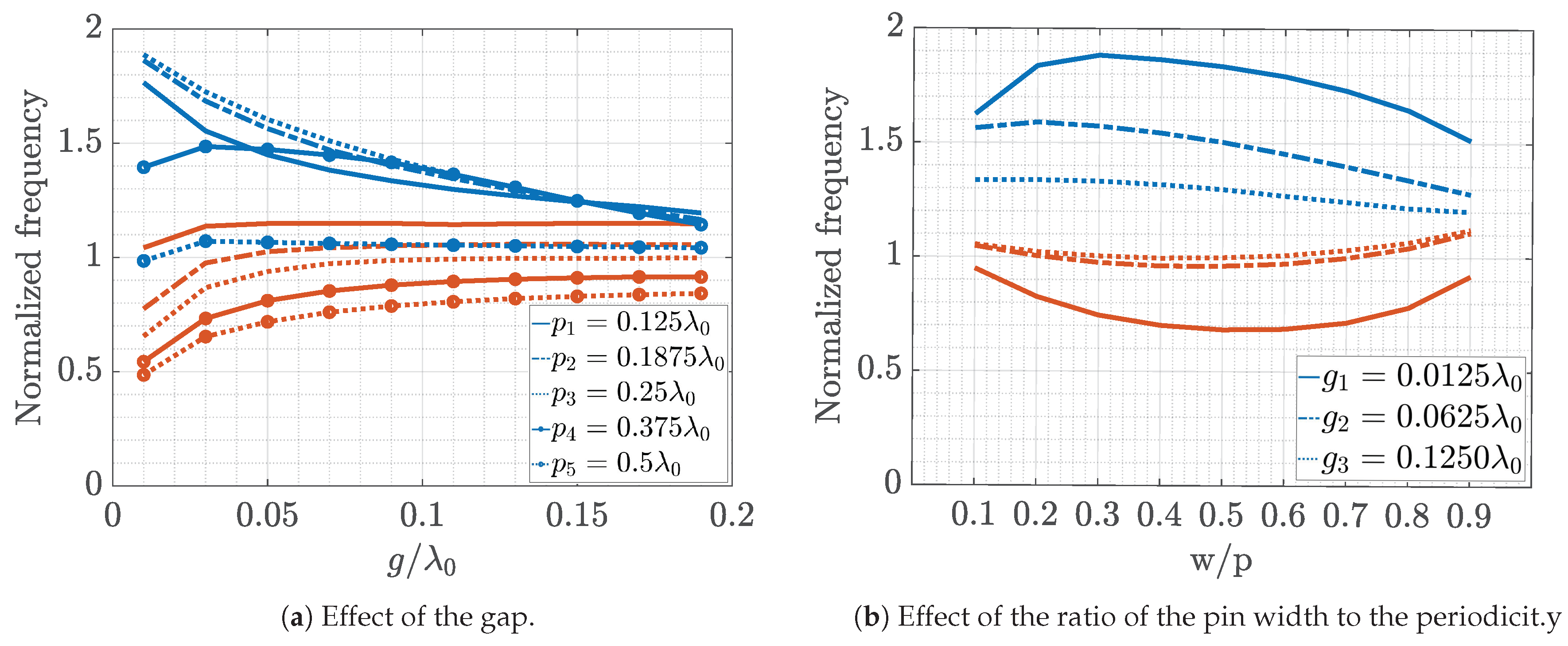
The first geometry to be analyzed is the the case of double pins with unequal heights, denoted as case
d (
Figure 1d). The parameters that vary are the gap
g for different periodicities and the effect of the relation
between the width
w of the pin and the period
p for different gap sizes. These parameters are analyzed for pin heights values
of 1.5 mm and 2 mm, and the results are shown in
Figure 7 and
Figure 8, respectively. In these figures, the blue curves represent the upper limit of the stopband, while the red curves represent the lower limit. For each value of the horizontal axis, a dispersion diagram has been calculated. The two represented points (red and blue) in vertical, correspond to the frequency where the stopband stats and the frequency where the stopband stops. For example, if you consider the dispersion diagram in
Figure 3 there is a frequency range where there are no modes. The maximum frequency of propagation of the first mode is the lower limit of the stop band, and the minimum frequency of propagation of the second mode is the upper limit.
The frequency is normalized to
, and the other parameters are normalized to
. The parameters that are not changed in the analysis correspond to the reference case. For the structure made with double pins of unequal heights, a reduction in the gap size always increases the stopband as shown in
Figure 7a and
Figure 8a. As the periodicity increases, the lower limit of the stopband decreases, and the upper limit of the stopband is not affected up to a value of the period after which it decreases. The ratio between the width of the pin and the periodicity
is optimum (maximizing the stopband) when the proportion is 1 to 2 (
Figure 7b and
Figure 8b).
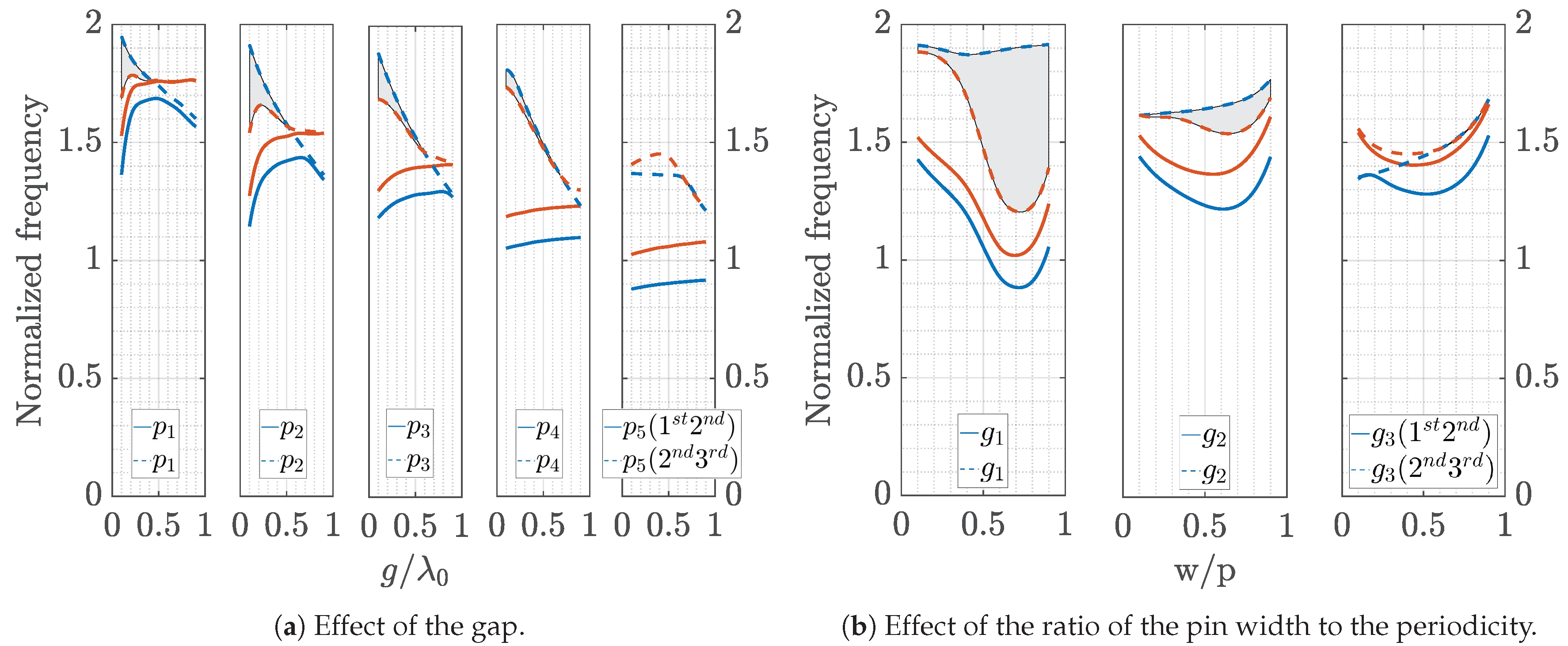
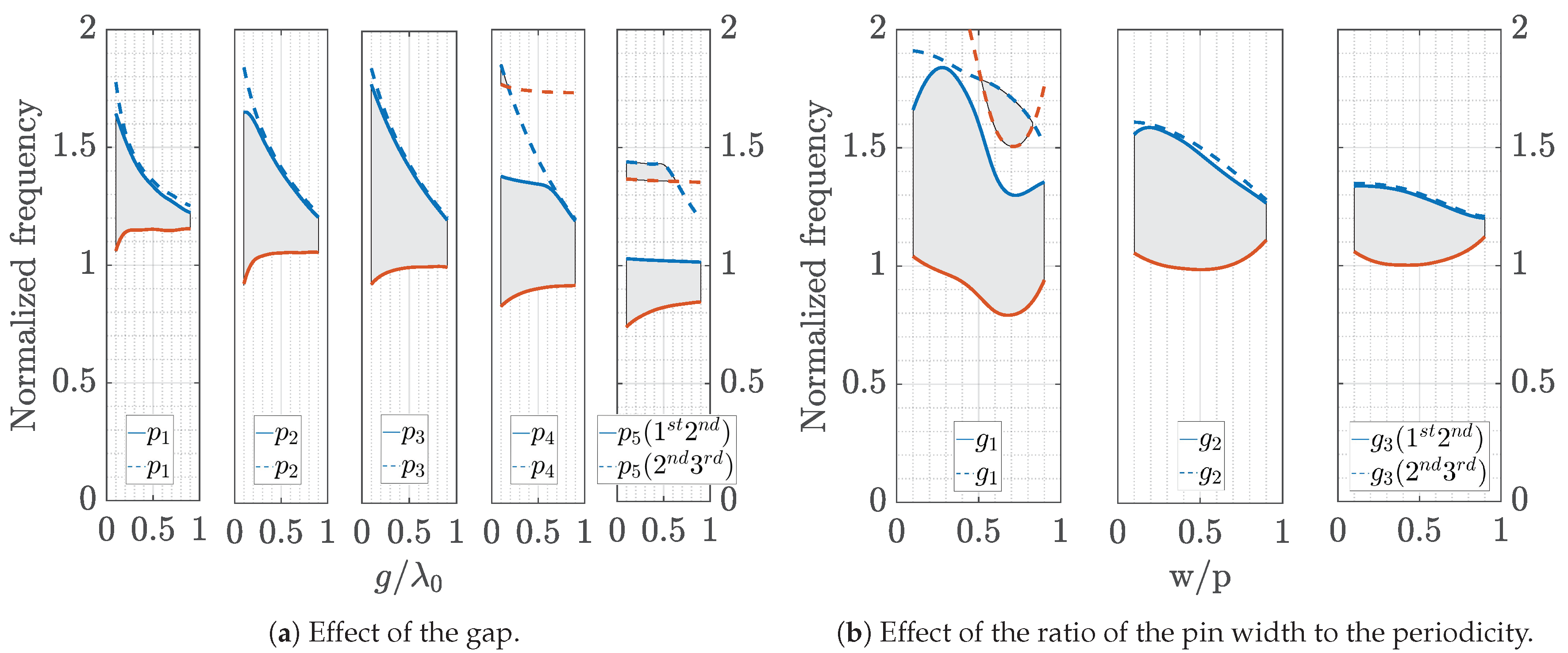
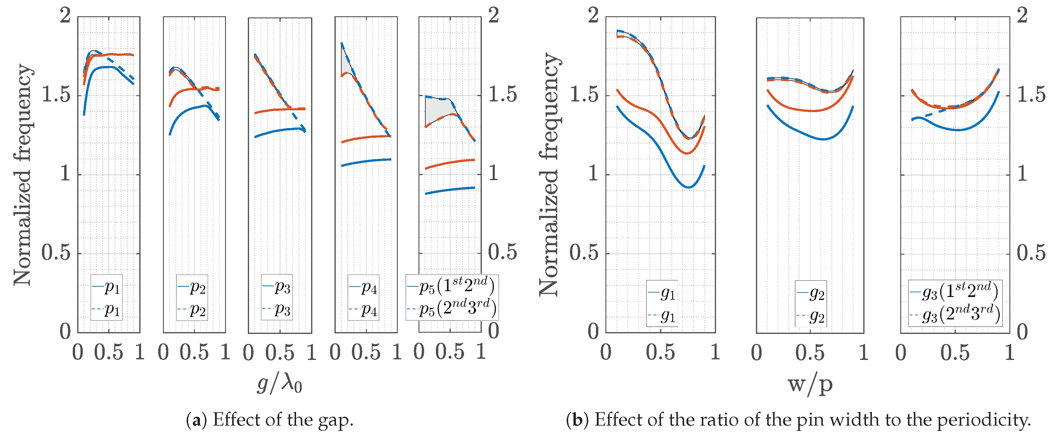
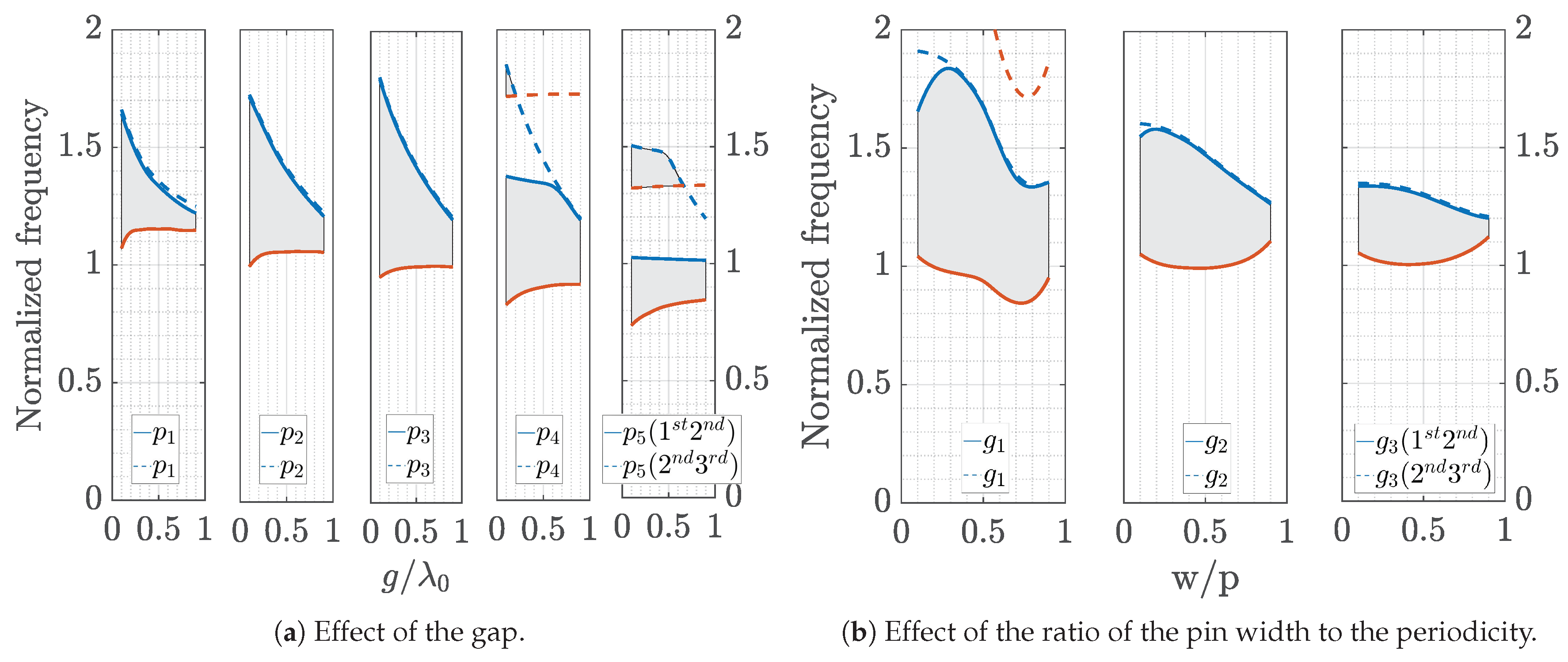
For the case of geometries with shifted pins (case
e), similar studies were carried out. In this case, we show the parametric effect when the pins have the same height and different heights. Two cases have been considered: pins shifted in just one direction (
Figure 9 and
Figure 10) and pins shifted in both directions (
Figure 11 and
Figure 12). In these figures, again the red lines represent the lower limit of the stopband, and the blue lines represent the upper limit. In addition, we have made use of subplots to better show the variation of the parameters. In these subplots, the dashed lines correspond to the stopbands formed between the second and third modes (represented by shaded areas), while the solid lines correspond to the stopband formed between the first and second modes. As concluded before, these geometries have very narrow or even nonexistent stopbands when
. However, when the pins have different sizes, stopbands appear and follow similar rules in terms of their parametric dependence as in the non shifted cases. Finally, the differences between the shifted cases in just one direction and in two directions are very small for the case when the pins have unequal heights but more important for the case when the pins have the same height (glide case).
4. Equivalent Refractive Index
Now, we proceed to analyze the effective refractive index of the first propagating mode of the previous structures. There are two main parameters we need to consider, namely the range of values achieved by the different structures (as all of them have the same basic element and periodicity) and how flat these lines are in frequency, as this will measure the dispersion of the element. The results can be used for designing wideband lenses [
21], making use of the low dispersion characteristic, or conversely to design a structure that requires a very dispersive unit cell as in [
15].
The calculation of the equivalent refraction index is made from the calculated dispersion diagram. In this calculation, we obtain the phase constant () of the first propagating mode. By dividing this phase constant by the free space propagation constant (), we obtain the equivalent refractive index.
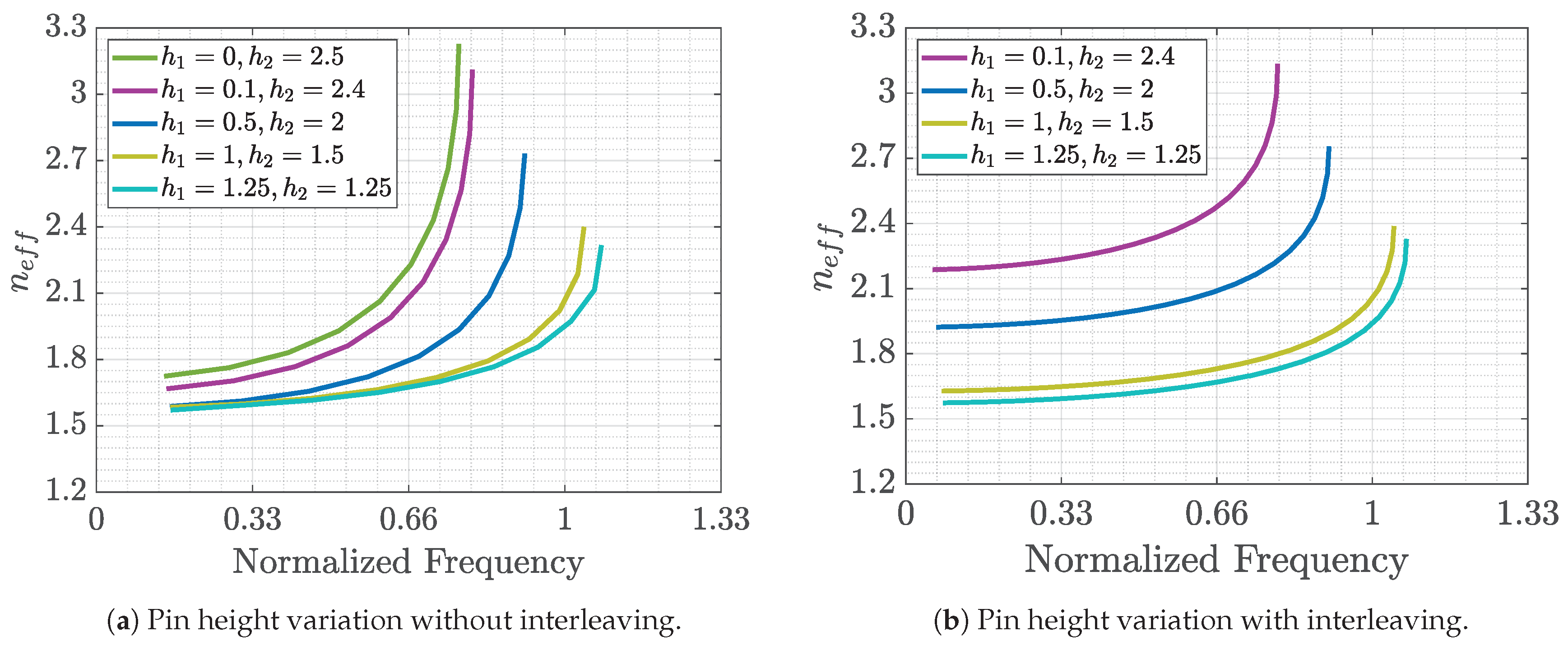
Figure 13a shows the effect of using the structures made with double pins with different heights in comparison with the case of a single pin. It is clear that with a single pin, we obtain higher refraction indices, but at the same time the structure is much more dispersive. Note that the less dispersive case occurs when both pins have exactly the same height.In all these figures the lines stop in the vertical axis due to the beginning of the stopband.
Figure 13b shows the analysis of the case with interleaving pins (case
f of
Figure 1). Once again, different heights of the pins have been considered. It is observed that changing the sizes of the consecutive pins leads to considerably higher equivalent refractive indices. This is explained by the fact that this is the only case where the air gap in between pins is not always located in the same position in the cross-section of the structure, as the gap position changes between consecutive pins. This somehow has an effect on the propagating field such that it does not encounter a straight path with only air. On the contrary, the propagating field necessarily finds the pins in its way, consequently increasing the equivalent refractive index. Another observation from these results is that with the interleaving pins, the mode is less dispersive.
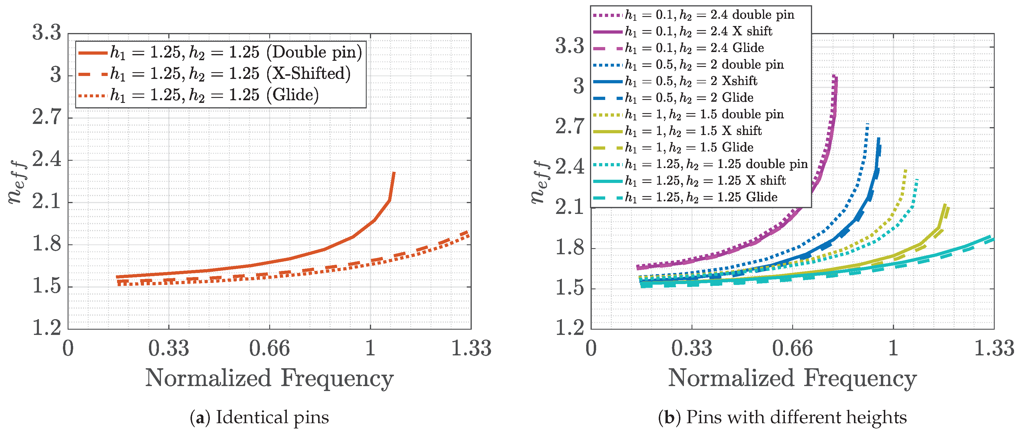
In
Figure 14, we show the effect of using higher symmetries in the unit cells of cases
b and
d of
Figure 1. For case
b (identical pins on the top and bottom), we can clearly see in
Figure 14a that a displacement of half the periodicity in one direction makes the structure less dispersive, as previously demonstrated for other types of unit cells [
12]. An extra displacement added in the perpendicular direction shas a small effect in this case, probably due to the fact that we are calculating the equivalent refractive index only in the first zone of the Brillouin diagram (
-
X). The achieved equivalent refraction indices are lower for the case with glide symmetry than for the case of the original pins without shifting. The same effect is observed for the case in which the top and bottom pins have different heights (
Figure 14b).
Effect of the Different Parameters on the Equivalent Refractive Index
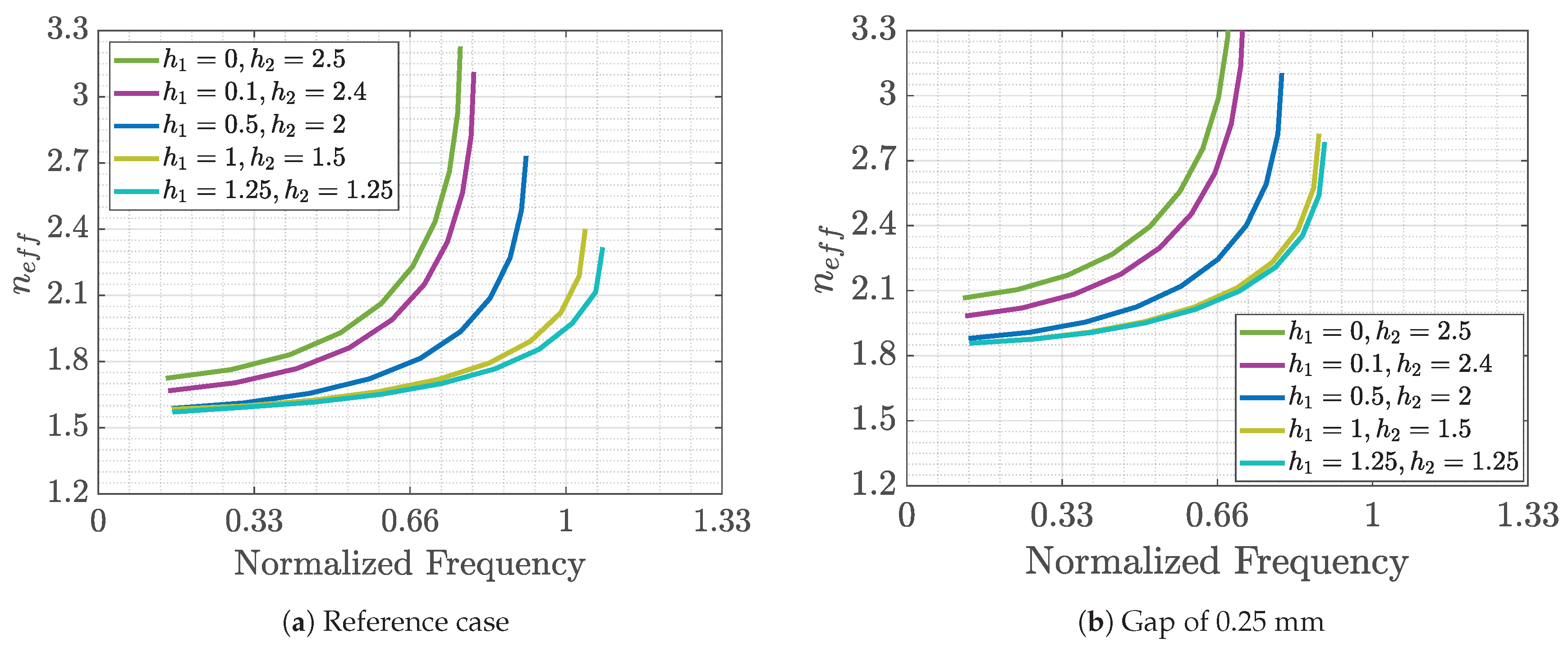
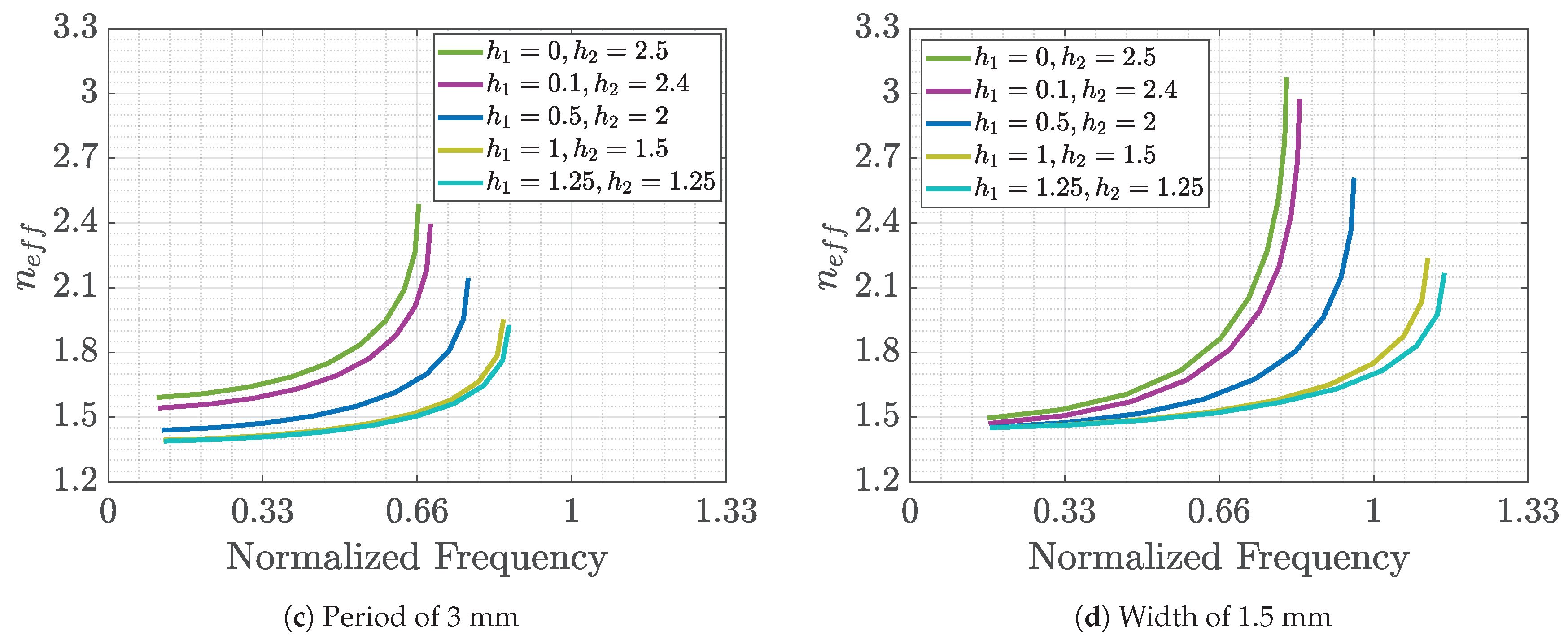
In this section, we present the effect of varying some of the parameters of the analyzed structures on the equivalent refractive index and the dispersion of the first mode. For this analysis, we individually change the size of the gap, the width of the pin and the periodicity, while the other parameters are kept constant at the initial reference values.
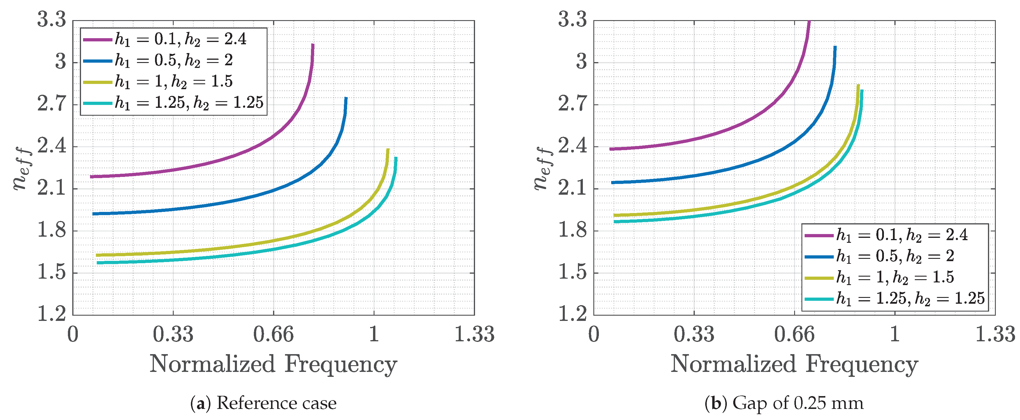
The first case to study is the structure with double pins of different heights. The reference case variables values in this case are
mm,
mm and
mm. The results are presented in
Figure 15. We can observe the following general conclusions: a decrease in the gap to one half of the value of the reference case (
Figure 15b) produces an increase in the equivalent refraction index for all the cases, probably as a consequence of the increase in the amount of metal with respect to air in the unit cell. On the other hand, an increase in the periodicity (from 2 to 3 mm) decreases the equivalent refractive index and makes the mode slightly less dispersive (
Figure 15c). Finally, the increase in the width of the pins to 1.5 mm decreases the minimum value of the refraction indices for all the cases independently of the heights (shown in
Figure 15d).
Considering the case
f from
Figure 1, i.e., interleaving pins with different heights, the effect of the parameters is shown in
Figure 16. In this case, a change in the gap size produces the same effects as those in the previous studied case. The use of a higher period is useful to obtain smaller values of the equivalent refraction indices but in this case does not show an improvement in the dispersion of the mode. Finally, the increase in the width of the pins reduces the dispersion in all the cases and has different consequences for the achieved values of the refraction indices depending on the heights. For identical pin heights, there is a reduction in the equivalent refractive index, while for unequal pins the index increases.
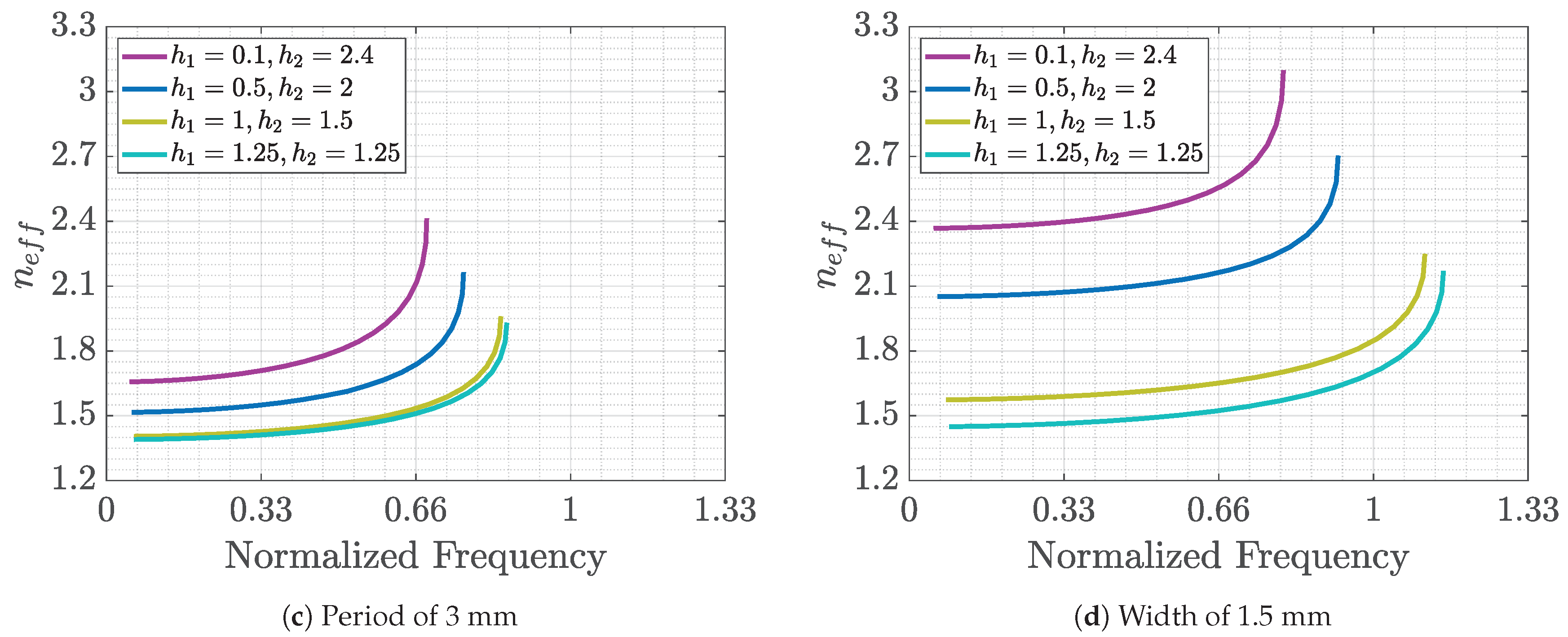
When the top and bottom pins are shifted to enable higher symmetries, the effect of varying the same parameters is presented in
Figure 17 for the case using pins with identical heights (glide case). The conclusions for this case are similar to those for the previous cases in terms of the variation in the gap and the periodicity (decreasing the gap or decreasing the periodicity increases the equivalent refractive index). On the other hand, the structure is almost insensitive to a variation in the width of the pins.
Finally, in the latter case, when we analyzed the behavior when the pins have unequal heights in the top and bottom layers, i.e., case
e from
Figure 1, the most significant conclusion derived from the results shown in
Figure 18 is the insensitivity to the variation in the width of the pins. In fact, with the increase in the width of the pins from 1 mm to 1.5 mm, all the analyzed cases converged to the same value of equivalent refractive index at low frequencies independently of their height or shift. On the other hand, for the other two parameters (the gap size and period), the conclusions were not different from those obtained for the previous cases.
5. Conclusions
In this work, different periodic structures combining pins inside parallel plate waveguide structures are analyzed. The pins are realized in several configurations including glide symmetry, shifting of the pins, asymmetries in the pin height and interleaving pins with different heights. The study focuses on dispersion diagrams. From the computed dispersion diagrams, information about the existence of a stopband for the parallel plate modes and its size and the propagation characteristics of the first mode are obtained. The propagation characteristics are studied as equivalent refraction indices as a function of frequency.
Initially, the effect of the different geometries considered (presented in
Figure 1) in these two aspects are studied. Concerning the stopband, the reference geometry (a single pin) produces a stopband covering a larger frequency range. On the other hand, glide symmetric structures do not have a stopband, while the cases combining pins with unequal heights always have stopbands (even if they are narrow).
The parametric studies carried out regarding this property confirm that in all cases with stopbands, a reduction in the gap size increases the bandwidth of the stopband and the ratio between the pin width and the period is relevant in determining this bandwidth. Similar conclusions were obtained in the past for the reference case.
With respect to the effective refractive index of the first propagating transverse electromagnetic mode (TEM), the main conclusions are that the structure with glide symmetry is less dispersive and that even for the case of using top and bottom pins with different heights, applying half-period shifts always reduces the dispersion. On the other side, the most dispersive case is the reference case with a single pin. Finally, when the pins are interleaved, the mode is also less dispersive than the reference structure and the equivalent refractive indices are larger.
The effect of the different parameters has also been evaluated from the perspective of propagation characteristics. As a global conclusion, a reduction in the gap or the period increases the refraction index. The effect of the width of the pins depends on the specific geometry.
Structures made with pins have been experimentally used and the manufacturing process is typically either a milling or 3D printing. When moving far up in frequency, long and thin pins can result in too fragile for manufacturing and the presented geometries based on the use of shorter pins can have advantages from this point of view.

 ,
, 


