Combining Nanofocused X-Rays with Electrical Measurements at the NanoMAX Beamline

 ,
,
Abstract
:
1. Introduction
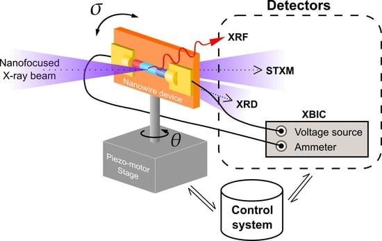
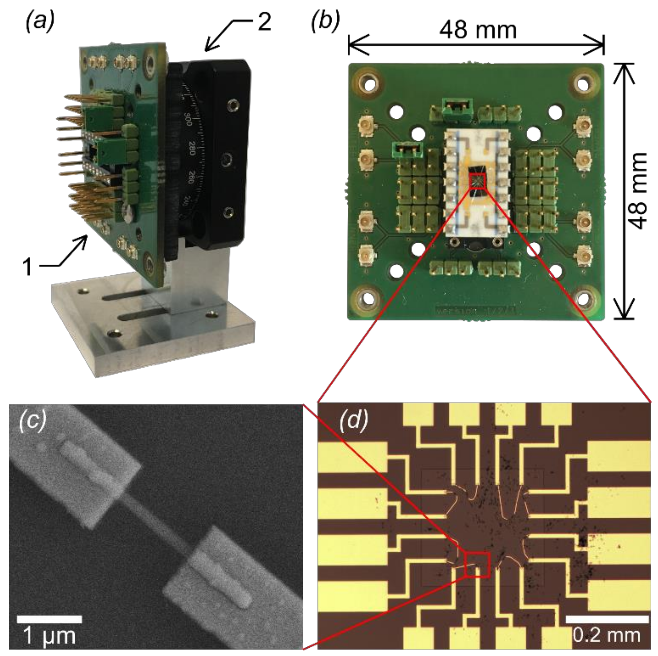
2. Methods
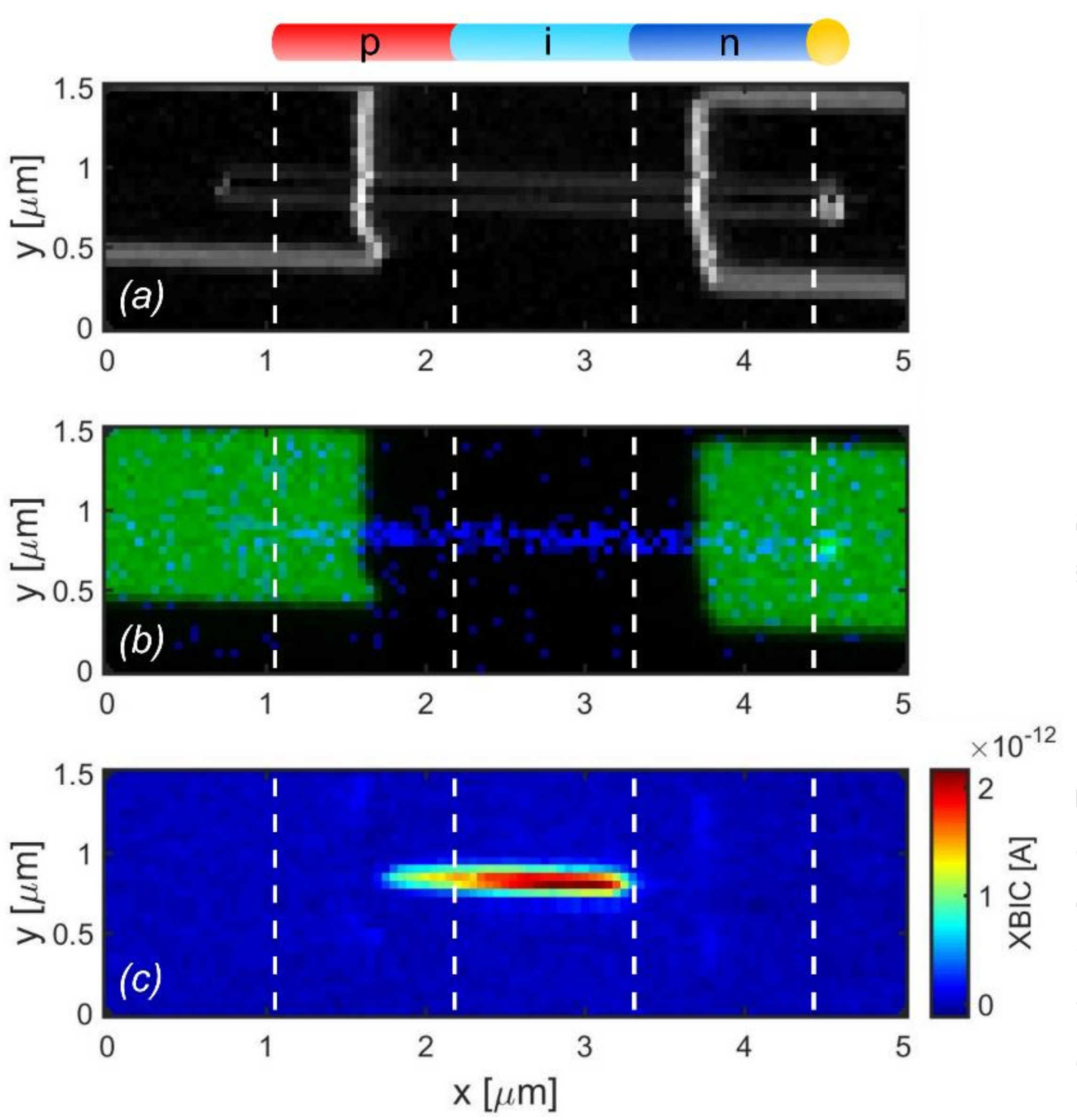
3. Results and Discussion
4. Conclusions
Supplementary Materials
Author Contributions
Funding
Acknowledgments
Conflicts of Interest
References
- Stuckelberger, M.; West, B.; Husein, S.; Guthrey, H.; Al-Jassim, M.; Chakraborty, R.; Buonassisi, T.; Maser, J.M.; Lai, B.; Stripe, B. Latest developments in the x-ray-based characterization of thin-film solar cells. In Proceedings of the Photovoltaic Specialist Conference (PVSC), New Orleans, LA, USA, 14–19 June 2015; pp. 1–6. [Google Scholar]
- Mimura, H.; Handa, S.; Kimura, T.; Yumoto, H.; Yamakawa, D.; Yokoyama, H.; Matsuyama, S.; Inagaki, K.; Yamamura, K.; Sano, Y.; et al. Breaking the 10-nm barrier in hard-X-ray focusing. Nat. Phys. 2010, 6, 122–125. [Google Scholar] [CrossRef]
- Döring, F.; Robisch, A.L.; Eberl, C.; Osterhoff, M.; Ruhlandt, A.; Liese, T.; Schlenkrich, F.; Hoffmann, S.; Bartels, M.; Salditt, T.; et al. Sub-5 nm hard x-ray point focusing by a combined Kirkpatrick-Baez mirror and multilayer zone plate. Opt. Express 2013, 21, 19311–19323. [Google Scholar]
- Holt, M.; Harder, R.; Winarski, R.; Rose, V. Nanoscale Hard X-Ray Microscopy Methods for Materials Studies. Annu. Rev. Mater. Res. 2013, 43, 183–211. [Google Scholar] [CrossRef]
- Etzelstorfer, T.; Sueess, M.J.; Schiefler, G.L.; Jacques, V.L.; Carbone, D.; Chrastina, D.; Isella, G.; Spolenak, R.; Stangl, J.; Sigg, H. Scanning X-ray strain microscopy of inhomogeneously strained Ge micro-bridges. J. Synchrotron Radiat. 2014, 21, 111–118. [Google Scholar] [CrossRef]
- Ulvestad, A.; Singer, A.; Cho, H.-M.; Clark, J.N.; Harder, R.; Maser, J.; Meng, Y.S.; Shpyrko, O.G. Single Particle Nanomechanics in Operando Batteries via Lensless Strain Mapping. Nano Lett. 2014, 14, 5123–5127. [Google Scholar] [CrossRef] [Green Version]
- Davtyan, A.; Lehmann, S.; Kriegner, D.; Zamani, R.R.; Dick, K.A.; Bahrami, D.; Al-Hassan, A.; Leake, S.J.; Pietsch, U.; Holý, V. Characterization of individual stacking faults in a wurtzite GaAs nanowire by nanobeam X-ray diffraction. J. Synchrotron Radiat. 2017, 24, 981–990. [Google Scholar] [CrossRef] [Green Version]
- Johannes, A.; Salomon, D.; Martinez-Criado, G.; Glaser, M.; Lugstein, A.; Ronning, C. In operando x-ray imaging of nanoscale devices: Composition, valence, and internal electrical fields. Sci. Adv. 2017, 3, eaao4044. [Google Scholar] [CrossRef]
- Chayanun, L.; Dagytė, V.; Troian, A.; Salomon, D.; Borgström, M.T.; Wallentin, J. Spectrally resolved x-ray beam induced current in a single InGaP nanowire. Nanotechnology 2018, 29, 454001. [Google Scholar] [CrossRef]
- Troian, A.; Otnes, G.; Zeng, X.; Chayanun, L.; Dagytė, V.; Hammarberg, S.; Salomon, D.; Timm, R.; Mikkelsen, A.; Borgström, M.T.; et al. Nanobeam X-ray Fluorescence Dopant Mapping Reveals Dynamics of in Situ Zn-Doping in Nanowires. Nano Lett. 2018, 18, 6461–6468. [Google Scholar] [CrossRef]
- Chayanun, L.; Otnes, G.; Troian, A.; Hammarberg, S.; Salomon, D.; Borgström, M.T.; Wallentin, J. Nanoscale mapping of carrier collection in single nanowire solar cells using X-ray beam induced current. J. Synchrotron Radiat. 2019, 26, 102–108. [Google Scholar] [CrossRef] [Green Version]
- Ahn, Y.H.; Tsen, A.W.; Kim, B.; Park, Y.W.; Park, J. Photocurrent Imaging of p−n Junctions in Ambipolar Carbon Nanotube Transistors. Nano Lett. 2007, 7, 3320–3323. [Google Scholar] [CrossRef] [PubMed]
- Hanoka, J.I. Electron-beam-induced current characterization of polycrystalline silicon solar cells. Sol. Cells 1980, 1, 123–139. [Google Scholar] [CrossRef]
- Ulvestad, A.; Singer, A.; Clark, J.N.; Cho, H.M.; Kim, J.W.; Harder, R.; Maser, J.; Meng, Y.S.; Shpyrko, O.G. Topological defect dynamics in operando battery nanoparticles. Science 2015, 348, 1344–1347. [Google Scholar] [CrossRef] [PubMed] [Green Version]
- Wallentin, J.; Osterhoff, M.; Salditt, T. In Operando X-Ray Nanodiffraction Reveals Electrically Induced Bending and Lattice Contraction in a Single Nanowire Device. Adv. Mater. 2016, 28, 1788–1792. [Google Scholar] [CrossRef] [PubMed]
- Karpov, D.; Liu, Z.; Rolo, T.d.S.; Harder, R.; Balachandran, P.V.; Xue, D.; Lookman, T.; Fohtung, E. Three-dimensional imaging of vortex structure in a ferroelectric nanoparticle driven by an electric field. Nat. Commun. 2017, 8, 280. [Google Scholar] [CrossRef]
- Lazarev, S.; Dzhigaev, D.; Bi, Z.; Nowzari, A.; Kim, Y.Y.; Rose, M.; Zaluzhnyy, I.A.; Gorobtsov, O.Y.; Zozulya, A.V.; Lenrick, F.; et al. Structural Changes in a Single GaN Nanowire under Applied Voltage Bias. Nano Lett. 2018, 18, 5446–5452. [Google Scholar] [CrossRef]
- Godard, P.; Carbone, G.; Allain, M.; Mastropietro, F.; Chen, G.; Capello, L.; Diaz, A.; Metzger, T.H.; Stangl, J.; Chamard, V. Three-dimensional high-resolution quantitative microscopy of extended crystals. Nat. Commun. 2011, 2, 568. [Google Scholar] [CrossRef]
- Hill, M.O.; Calvo-Almazan, I.; Allain, M.; Holt, M.V.; Ulvestad, A.; Treu, J.; Koblmüller, G.; Huang, C.; Huang, X.; Yan, H.; et al. Measuring Three-Dimensional Strain and Structural Defects in a Single InGaAs Nanowire Using Coherent X-ray Multiangle Bragg Projection Ptychography. Nano Lett. 2018, 18, 811–819. [Google Scholar] [CrossRef] [Green Version]
- Johansson, U.; Vogt, U.; Mikkelsen, A. NanoMAX: A hard x-ray nanoprobe beamline at MAX IV. SPIE 2013, 8851, 88510L. [Google Scholar]
- Eriksson, M.; Malmgren, L.; Al-Dmour, E.; Thorin, S.; Johansson, M.; Leemann, S.; Andersson, Å; Tavares, P. Commissioning of the MAX IV light source. In Proceedings of the IPAC 2016, Busan, Korea, 8–13 May 2016. [Google Scholar]
- Memisevic, E.; Hellenbrand, M.; Lind, E.; Persson, A.R.; Sant, S.; Schenk, A.; Svensson, J.; Wallenberg, R.; Wernersson, L.-E. Individual Defects in InAs/InGaAsSb/GaSb Nanowire Tunnel Field-Effect Transistors Operating below 60 mV/decade. Nano Lett. 2017, 17, 4373–4380. [Google Scholar] [CrossRef] [Green Version]
- Otnes, G.; Barrigón, E.; Sundvall, C.; Svensson, K.E.; Heurlin, M.; Siefer, G.; Samuelson, L.; Åberg, I.; Borgström, M.T. Understanding InP Nanowire Array Solar Cell Performance by Nanoprobe-Enabled Single Nanowire Measurements. Nano Lett. 2018, 18, 3038–3046. [Google Scholar] [CrossRef] [PubMed]
- Bunk, O.; Bech, M.; Jensen, T.H.; Feidenhans’l, R.; Binderup, T.; Menzel, A.; Pfeiffer, F. Multimodal x-ray scatter imaging. New J. Phys. 2009, 11, 123016. [Google Scholar] [CrossRef]
- Rodenburg, J.M. Ptychography and Related Diffractive Imaging Methods. Adv. Imaging Electron Phys. 2008, 150, 87–184. [Google Scholar]
- Rodnyi, P.A. Physical Processes in Inorganic Scintillators; CRC press: Boca Raton, FL, USA, 1997. [Google Scholar]
- Nikl, M. Scintillation detectors for x-rays. Meas. Sci. Technol. 2006, 17, R37–R54. [Google Scholar] [CrossRef]
- Lecoq, P.; Gektin, A.; Korzhik, M. Inorganic Scintillators for Detector Systems: Physical Principles and Crystal Engineering; Springer: Berlin/Heidelberg, Germany, 2016. [Google Scholar]
- Eymery, J.; Rieutord, F.; Favre-Nicolin, V.; Robach, O.; Niquet, Y.-M.; Fröberg, L.; Mårtensson, T.; Samuelson, L. Strain and Shape of Epitaxial InAs/InP Nanowire Superlattice Measured by Grazing Incidence X-ray Techniques. Nano Lett. 2007, 7, 2596–2601. [Google Scholar] [CrossRef] [PubMed]
- Diaz, A.; Mocuta, C.; Stangl, J.; Mandl, B.; David, C.; Vila-Comamala, J.; Chamard, V.; Metzger, T.H.; Bauer, G. Coherent diffraction imaging of a single epitaxial InAs nanowire using a focused x-ray beam. Phys. Rev. B 2009, 79, 125324. [Google Scholar] [CrossRef] [Green Version]
- Newton, M.C.; Leake, S.J.; Harder, R.; Robinson, I.K. Three-dimensional imaging of strain in a single ZnO nanorod. Nat. Mater. 2009, 9, 120. [Google Scholar] [CrossRef]
- Favre-Nicolin, V.; Mastropietro, F.; Eymery, J.; Camacho, D.; Niquet, Y.M.; Borg, B.M.; Messing, M.E.; Wernersson, L.E.; Algra, R.E.; Bakkers, E.P.A.M.; et al. Analysis of strain and stacking faults in single nanowires using Bragg coherent diffraction imaging. New J. Phys. 2010, 12, 035013. [Google Scholar] [CrossRef]
- Haag, S.T.; Richard, M.-I.; Welzel, U.; Favre-Nicolin, V.; Balmes, O.; Richter, G.; Mittemeijer, E.J.; Thomas, O. Concentration and Strain Fields inside a Ag/Au Core–Shell Nanowire Studied by Coherent X-ray Diffraction. Nano Lett. 2013, 13, 1883–1889. [Google Scholar] [CrossRef]
- Stankevič, T.; Mickevičius, S.; Schou Nielsen, M.; Kryliouk, O.; Ciechonski, R.; Vescovi, G.; Bi, Z.; Mikkelsen, A.; Samuelson, L.; Gundlach, C. Measurement of strain in InGaN/GaN nanowires and nanopyramids. J. Appl. Crystallogr. 2015, 48, 344–349. [Google Scholar] [CrossRef]
- Schroth, P.; Jakob, J.; Feigl, L.; Mostafavi Kashani, S.M.; Vogel, J.; Strempfer, J.; Keller, T.F.; Pietsch, U.; Baumbach, T. Radial Growth of Self-Catalyzed GaAs Nanowires and the Evolution of the Liquid Ga-Droplet Studied by Time-Resolved in Situ X-ray Diffraction. Nano Lett. 2018, 18, 101–108. [Google Scholar] [CrossRef] [PubMed]
- Wallentin, J.; Osterhoff, M.; Wilke, R.N.; Persson, K.-M.; Wernersson, L.-E.; Sprung, M.; Salditt, T. Hard X-ray Detection Using a Single 100 nm Diameter Nanowire. Nano Lett. 2014, 14, 7071–7076. [Google Scholar] [CrossRef] [PubMed]
- Hieslmair, H.; Istratov, A.A.; Sachdeva, R.; Weber, E.R. New Synchrotron-Radiation-Based Technique to Study Localized Defects in Silicon: ‘EBIC’ with X-ray Excitation; LBNL/ALS--43453; Ernest Orlando Lawrence Berkeley National Lab.: Berkeley, CA, USA, 2000; Available online: https://inis.iaea.org/search/search.aspx?orig_q=RN:33061273 (accessed on 15 August 2019).
- Vyvenko, O.F.; Buonassisi, T.; Istratov, A.A.; Weber, E.R. X-ray beam induced current/microprobe x-ray fluorescence: Synchrotron radiation-based x-ray microprobe techniques for analysis of the recombination activity and chemical nature of metal impurities in silicon. J. Phys. Condens. Matter 2004, 16, S141. [Google Scholar] [CrossRef]
- Buonassisi, T.; Heuer, M.; Vyvenko, O.F.; Istratov, A.A.; Weber, E.R.; Cai, Z.; Lai, B.; Ciszek, T.F.; Schindler, R. Applications of synchrotron radiation X-ray techniques on the analysis of the behavior of transition metals in solar cells and single-crystalline silicon with extended defects. Phys. B: Condens. Matter 2003, 340–342, 1137–1141. [Google Scholar] [CrossRef]
- Buonassisi, T.; Istratov, A.A.; Pickett, M.D.; Marcus, M.A.; Hahn, G.; Riepe, S.; Isenberg, J.; Warta, W.; Willeke, G.; Ciszek, T.F.; et al. Quantifying the effect of metal-rich precipitates on minority carrier diffusion length in multicrystalline silicon using synchrotron-based spectrally resolved x-ray beam-induced current. Appl. Phys. Lett. 2005, 87, 044101. [Google Scholar] [CrossRef] [Green Version]
- Seifert, W.; Vyvenko, O.; Arguirov, T.; Kittler, M.; Salome, M.; Seibt, M.; Trushin, M. Synchrotron-based investigation of iron precipitation in multicrystalline silicon. Superlattices Microstruct. 2009, 45, 168–176. [Google Scholar] [CrossRef]
- West, B.; Husein, S.; Stuckelberger, M.; Lai, B.; Maser, J.; Stripe, B.; Rose, V.; Guthrey, H.; Al-Jassim, M.; Bertoni, M. Correlation between grain composition and charge carrier collection in Cu(In,Ga)Se2 solar cells. In Proceedings of the 2015 IEEE 42nd Photovoltaic Specialist Conference (PVSC), New Orleans, LA, USA, 14–19 June 2015; pp. 1–4. [Google Scholar]
- Stuckelberger, M.; Nietzold, T.; Hall, G.N.; West, B.; Werner, J.; Niesen, B.; Ballif, C.; Rose, V.; Fenning, D.P.; Bertoni, M.I. Elemental distribution and charge collection at the nanoscale on perovskite solar cells. In Proceedings of the 2016 IEEE 43rd Photovoltaic Specialists Conference (PVSC), Portland, OR, USA, 5–10 June 2016; pp. 1191–1196. [Google Scholar]
- Osterhoff, M.; Eberl, C.; Döring, F.; Wilke, R.N.; Wallentin, J.; Krebs, H.-U.; Sprung, M.; Salditt, T. Towards multi-order hard X-ray imaging with multilayer zone plates. J. Appl. Crystallogr. 2015, 48, 116–124. [Google Scholar] [CrossRef] [Green Version]
- Bajt, S.; Prasciolu, M.; Fleckenstein, H.; Domaracký, M.; Chapman, H.N.; Morgan, A.J.; Yefanov, O.; Messerschmidt, M.; Du, Y.; Murray, K.T.; et al. X-ray focusing with efficient high-NA multilayer Laue lenses. Light: Sci. Amp; Appl. 2018, 7, 17162. [Google Scholar] [CrossRef]
- Bell, P.; Hardion, V.; Jamróz, J.; Lidón-Simon, J. Control and Data Acquisition Using TANGO and SARDANA at the Nanomax Beamline at MAX IV. In Proceedings of the 16th International Conference on Accelerator and Large Experimental Control Systems, Barcelona, Spain, 8–13 October 2017; pp. 900–904. [Google Scholar]
- Spear, J.D. Shot noise in x-ray measurements with p-i-n diodes. Rev. Sci. Instrum. 2005, 76, 076101. [Google Scholar] [CrossRef]
- Stuckelberger, M.; West, B.; Nietzold, T.; Lai, B.; Maser, J.M.; Rose, V.; Bertoni, M.I. Engineering solar cells based on correlative X-ray microscopy. J. Mater. Res. 2017, 32, 1825–1854. [Google Scholar] [CrossRef]
- Yang, C.; Pyry, K.; Mats-Erik, P.; Nicklas, A. Optimization of the short-circuit current in an InP nanowire array solar cell through opto-electronic modeling. Nanotechnology 2016, 27, 435404. [Google Scholar]
- Alig, R.C.; Bloom, S. Secondary-electron-escape probabilities. J. Appl. Phys. 1978, 49, 3476–3480. [Google Scholar] [CrossRef]
- Chahine, G.A.; Richard, M.-I.; Homs-Regojo, R.A.; Tran-Caliste, T.N.; Carbone, D.; Jacques, V.L.R.; Grifone, R.; Boesecke, P.; Katzer, J.; Costina, I.; et al. Imaging of strain and lattice orientation by quick scanning X-ray microscopy combined with three-dimensional reciprocal space mapping. J. Appl. Crystallogr. 2014, 47, 762–769. [Google Scholar] [CrossRef]
- Wallentin, J.; Jacobsson, D.; Osterhoff, M.; Borgström, M.T.; Salditt, T. Bending and Twisting Lattice Tilt in Strained Core–Shell Nanowires Revealed by Nanofocused X-ray Diffraction. Nano Lett. 2017, 17, 4143–4150. [Google Scholar] [CrossRef]


© 2019 by the authors. Licensee MDPI, Basel, Switzerland. This article is an open access article distributed under the terms and conditions of the Creative Commons Attribution (CC BY) license (http://creativecommons.org/licenses/by/4.0/).
Share and Cite
Chayanun, L.; Hammarberg, S.; Dierks, H.; Otnes, G.; Björling, A.; Borgström, M.T.; Wallentin, J. Combining Nanofocused X-Rays with Electrical Measurements at the NanoMAX Beamline. Crystals 2019, 9, 432. https://doi.org/10.3390/cryst9080432
Chayanun L, Hammarberg S, Dierks H, Otnes G, Björling A, Borgström MT, Wallentin J. Combining Nanofocused X-Rays with Electrical Measurements at the NanoMAX Beamline. Crystals. 2019; 9(8):432. https://doi.org/10.3390/cryst9080432
Chicago/Turabian StyleChayanun, Lert, Susanna Hammarberg, Hanna Dierks, Gaute Otnes, Alexander Björling, Magnus T Borgström, and Jesper Wallentin. 2019. "Combining Nanofocused X-Rays with Electrical Measurements at the NanoMAX Beamline" Crystals 9, no. 8: 432. https://doi.org/10.3390/cryst9080432