Commentary

Thin-Film Optical Devices Based on Transparent Conducting Oxides: Physical Mechanisms and Applications

Department of Electronics, Pusan National University, Pusan 46241, Korea
*
Author to whom correspondence should be addressed.
Crystals 2019, 9(4), 192; https://doi.org/10.3390/cryst9040192
Submission received: 25 February 2019 / Revised: 24 March 2019 / Accepted: 27 March 2019 / Published: 3 April 2019
(This article belongs to the Special Issue Thin Film Transistor)

Abstract

:
This paper provides a review of optical devices based on a wide band-gap transparent conducting oxide (TCO) while discussing related physical mechanisms and potential applications. Intentionally using a light-induced metastability mechanism of oxygen defects in TCOs, it is allowed to detect even visible lights, eluding to a persistent photoconductivity (PPC) as an optical memory action. So, this PPC phenomenon is naturally useful for TCO-based optical memory applications, e.g., optical synaptic transistors, as well as photo-sensors along with an electrical controllability of a recovery speed with gate pulse or bias. Besides the role of TCO channel layer in thin-film transistor structure, a defective gate insulator can be another approach for a memory operation with assistance for gate bias and illuminations. In this respect, TCOs can be promising materials for a low-cost transparent optoelectronic application.

1. Introduction

Transparent conducting oxides (TCOs) are getting an intensive interest for a transparent display application since they exhibit high transparency arising from a wide band-gap [1,2,3,4,5]. Besides its high transparency, a low-temperature processability is another advantage suitable for display applications where a low melting-point substrate with a high flexibility is usually used [3,6,7]. This feature is mainly related to its isotropic bonding mechanism based on the overlap of s-orbitals for the conduction band, which is insensitive to bonding direction, providing high electron mobility. So, it can easily be connected even in a low-temperature fabrication. On the other hand, the conventional thin-film material for displays, e.g., amorphous silicon, has an anisotropic bonding nature due to its sp3 hybrid orbitals with a strong bonding directivity, thus difficult to be crystallized in a low temperature [6,8,9]. In this respect, TCOs have been considered as a strong candidate in futuristic electronics, including transparent and flexible displays [5,7,10,11,12,13].
However, TCOs have optical stability issues associated with oxygen defects, e.g., oxygen vacancies and interstitials even though these defects are playing the role as an electron donor to control the film conductivity during the deposition [8,14,15,16]. For example, the oxygen vacancy as an empty place of a bonding oxygen can be ionized under light with a relevant photon energy, giving free electrons [17,18,19,20]. And the deionization process, followed after removal of a light source, tends to be much slower than the ionization, suggesting a metastability, i.e., persistent photoconductivity (PPC) [21,22]. Moreover, this kind of metastable defects can also be newly created especially under a high energy illumination, e.g., ultra-violet (UV) [19,23]. From these circumstances, these oxygen defects are basically problematic, but simultaneously useful for photo-sensing applications if that slow recovery is overcome.
In this paper, we present a review of optical devices based on TCO thin films in terms of respective physical mechanisms and related applications. The key physical mechanism of TCO-based optical devices is associated with oxygen defects within TCO films (see Section 2). Since they are located within the band-gap, their location in energy is relevant to detect even visible light. This implies their optical ionization is a key absorption mechanism of photo-sensors. On the other hand, the deionization process after the removal of light, i.e., recovering process, is very slow in comparison with the ionization process, suggesting the PPC. This PPC is problematic for photo-sensors because it especially increases a dark signal level after the illumination, which can be overcome with applying a positive gate pulse [25]. As a positive aspect of the PPC, however, it is a memory action naturally induced under illumination. Indeed, optical memory devices, such as optical synaptic transistors, where a TCO (e.g., In-Ga-Zn-O, In-Zn-O, etc.) is a channel absorption layer, have been introduced using this phenomenon [26]. In another type of TCO-based optical synaptic thin-film transistors, a gate insulator, e.g., chitosan electrolyte or HfOx, with mobile impurities or traps, is incorporated into a field-effect transistor structure along with a TCO channel layer, leading to a more distinguishable hysteresis for a strong memory action under light, depending on the polarity of gate bias [27,28]. In these respects, TCOs can be promising materials for a low-cost transparent optoelectronic application besides their basic usage for a transparent display application. These are discussed in Section 3.

2. Optical Properties and Instability Mechanism

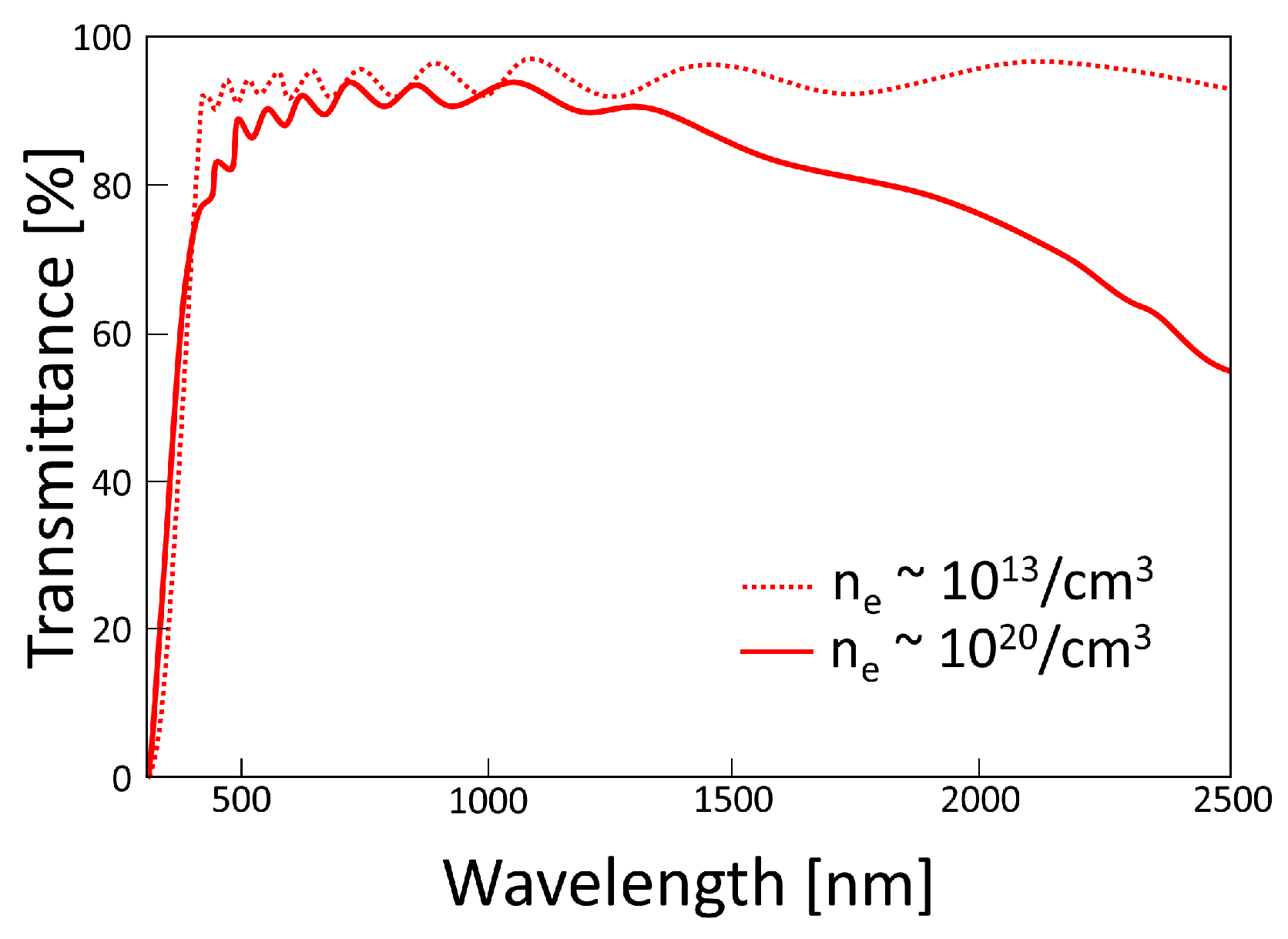
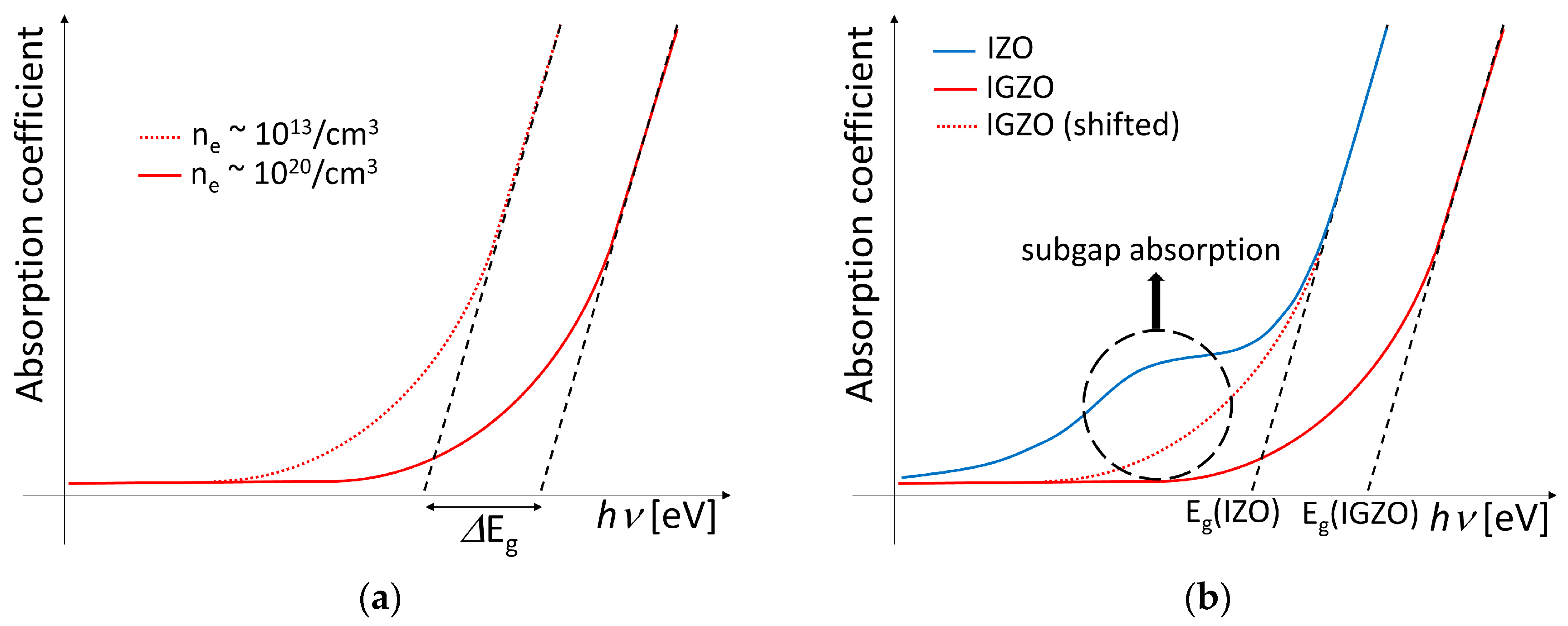
2.1. Basic Optical Properties

TCOs have been considered as a strong candidate in futuristic electronics, including transparent and flexible displays, thanks to their high transparency (>80% in visible range) due to a large bandgap and a high mobility even under low temperature fabrication process associated with isotropic bonding nature of orbitals for conduction band bottom. However, a large carrier concentration, which is desired for a good conductivity, is thought to be an issue in optical transparency. Within the partially-filled conduction band, an intra-band transition occurs, thus an increase of optical absorption at long wavelengths [29,30,31]. Figure 1 shows a decrease in the transmission rate for IGZO films with a high carrier concentration. In contrast, at short wavelengths, this partially-filled conduction band gives rise to increasing the effective bandgap, as shown in Figure 2a, thus a blue-shifted optical absorption edge energy, which is called as a Burstein-Moss (BM) effect [24,32].
Different from these kinds of absorption related to carrier excitation, a subgap optical absorption also occurs due to ionization of subgap states [19,20,21,33,34]. Figure 2b depicts the conceptual Tauc plot for comparing amorphous IZO’s and amorphous IGZO’s subgap optical absorptions. The subgap absorption in TCOs is suggested to be mainly dependent on the presence of oxygen defects. As described in Figure 2b, the subgap absorption in IZO is higher compared to IGZO because the former contains relatively more oxygen defects [25,35]. The subgap absorption is not only problematic for transparency, it also causes interesting electrical issues, such as increase of carrier concentration, leading to an increase of the film conductivity, and a threshold voltage shift in the TFTs, electrical hysteresis, and the PPC. In this respect, we will further discuss this subgap absorption especially related to oxygen defects, and respective instability mechanisms under illumination in the following section.

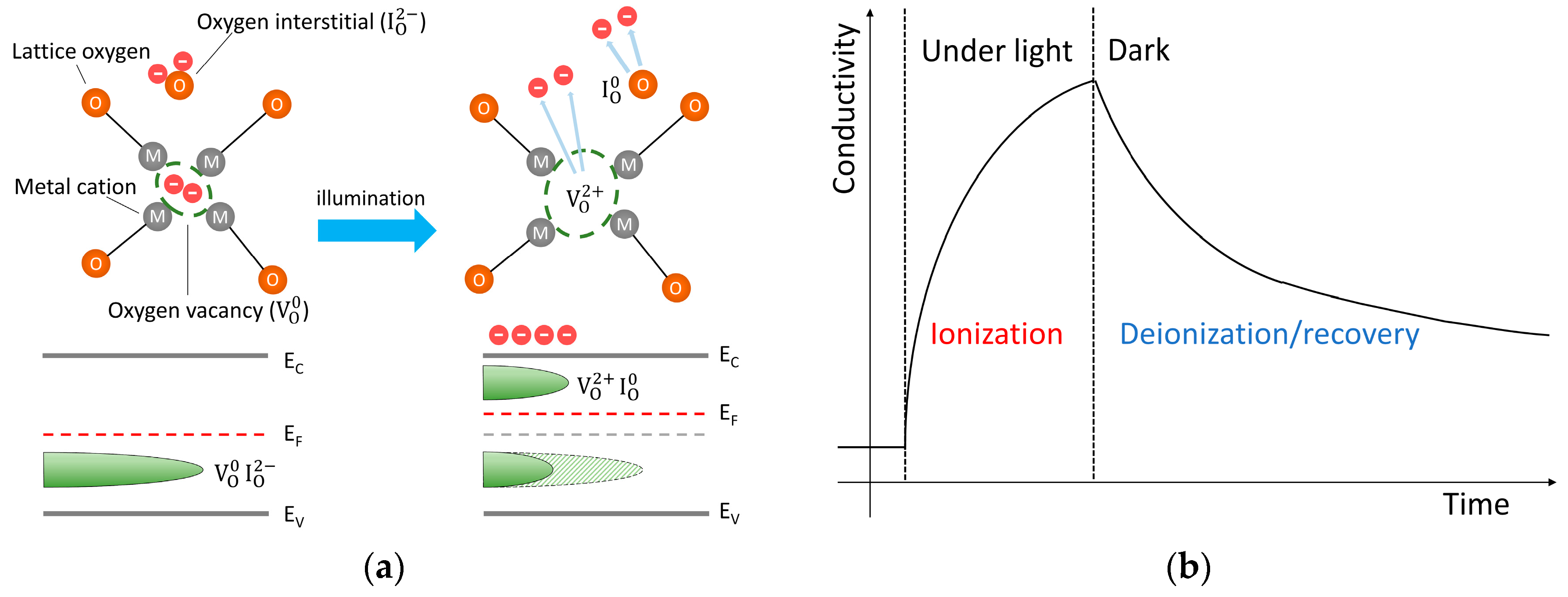
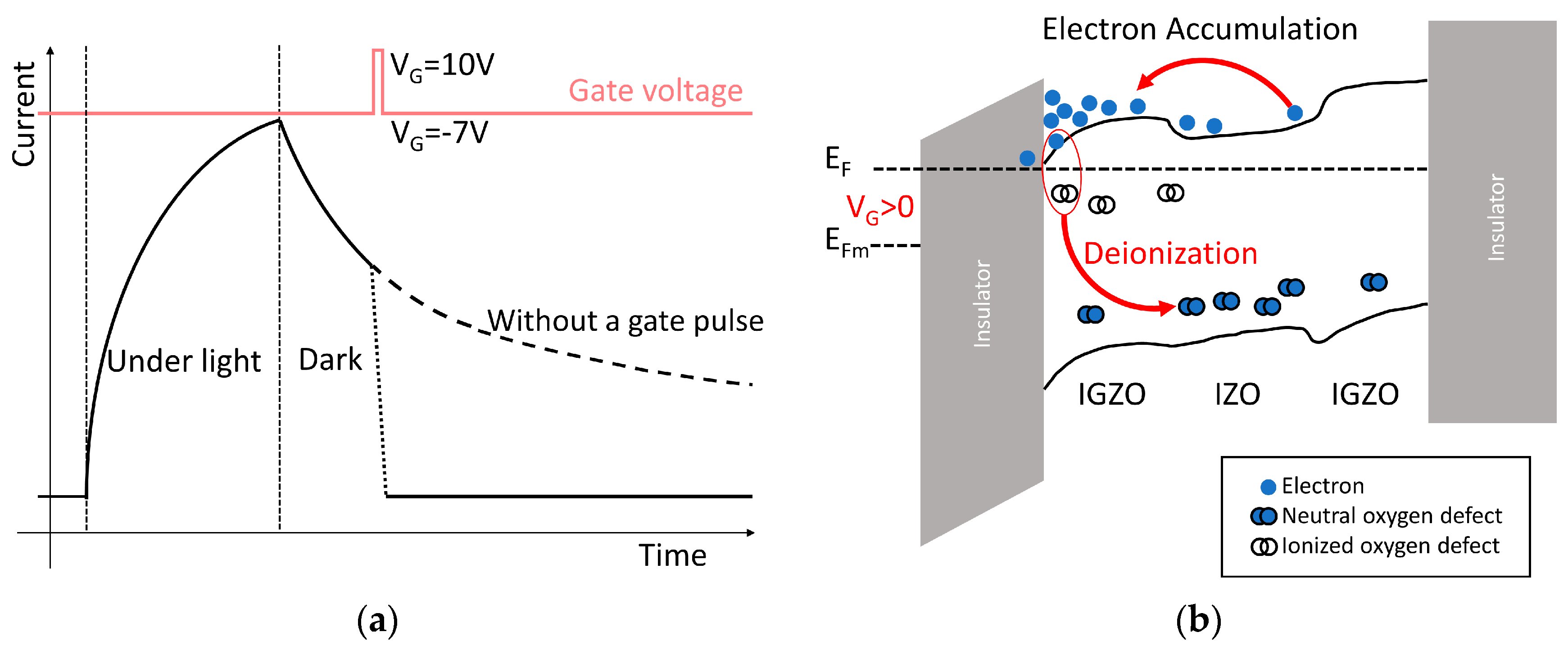
2.2. Oxygen Defects and Optical Instability Mechanisms

Oxygen defects, such as oxygen vacancies (VO) and oxygen interstitial (IO), reside within deep subgap states, eluding to a sub-gap optical absorption even under a visible light (i.e., hν < Eg) while being ionized in the following processes, respectively, V O V O 2 + + 2 e and I O 2 I O 0 + 2 e [21,30,36,37,38,39]. The excess electrons emitted during ionization process of oxygen defects contribute to the carrier concentration, increasing Fermi energy (EF) and conductivity of the film. This affects negative threshold voltage shift in the operation of the TFTs, where TCOs are used for the channel layer, thus an increase of drain current [40,41,42,43]. Note that the density of oxygen defects can be controlled by changing the oxygen gas flow rate during the film deposition process [6,15,21]. With a sufficiently high oxygen flow rate, oxygen defects can be minimized whereas oxygen interstitials can newly be created with a very high oxygen flow rate, so that an optimization is needed. However, for an optical application, the presence of these defects is intentionally used as discussed here.
As illustrated in Figure 3a, interestingly, however, the ionization of oxygen defects involves relaxation of the lattice, suggesting a higher activation energy of the ionized defects compared to the neutral state defects [21,44,45]. It implies the ionized oxygen defects as metastable states. This metastability limits the recombination rate of the ionized defects, so the recovery process shows slower speed compared to the ionization. And this makes photo-enhanced conductivity persist for a relatively long time, depending on the temperature and bias condition, which is called PPC (see Figure 3b) [5,21,22,46]. This recovery trend is quantitatively analyzed by a stretched exponential function (SEF), as follows.
F ( t ) = A eff exp ( ( t τ eff ) β )
where Aeff is a weighting amplitude, τeff is an effective time constant, β is a stretched exponent whose range is from zero to unity. Note that Aeff is generally normalized as unity since it is related to the light intensity but not the photon energy. The PPC, which is a kind of optoelectronic hysteresis, is a memory action naturally induced with illumination. It implies a possibility for memory application without an additional capacitor structure. And the increase of film conductivity under illumination implies that TCO films can be used for a photo-sensor application as long as the PPC is eliminated to reset the reference signal level for a periodic sensing as a function of time. These operating concepts of devices are illustrated in Figure 4. And we discuss them in the following section.

3. Optoelectronic Applications

3.1. Photo-Sensors

In the previous section, it is shown that the TCO-based thin film can be applied for photo-sensors, detecting even visible lights which have a lower photon energy compared to the bandgap energy. With this feature, the TCO-based visible light photo-sensors can be integrated into transparent electronics. However, the PPC, associated with oxygen defects of the TCOs, increases the dark signal level after illumination (i.e., reference signal level), which can be problematic for a periodic photo-sensing, as mentioned in the previous section. In this section, we discuss the TCO-based photo-sensors with a possible solution for suppressing the PPC-related issue.
As an example seen in Figure 5, Sanghun Jeon et al. demonstrated a TCO-based device for photo-sensor arrays [25]. Here, an IZO channel layer, which has a relatively large amount of oxygen defects and respective high light-sensitivity, is employed for the main absorption layer. And two IGZO layers are adapted above and below the IZO layer to compensate a negative threshold voltage of the IZO layer-only TFT. So, it is found that the threshold voltage of IGZO/IZO/IGZO TFT is about 0 V. The authors set the device operating under a negative gate bias (VGS = −7 V) and positive drain bias (VDS = 10 V) for a distinguishable sensing level, raising Iphoto/Idark ratio, where Iphoto is the photocurrent and Idark is the dark current. When the device is illuminated, the oxygen defects in the channel layers are ionized, and simultaneously band-to-band excitation occurs, thus a free electron generation and raise of Fermi level. These cause negative shift of the threshold voltage, which is observable with an increase of the drain-source current. But the PPC is naturally occurred in the TCO films, and even reinforced by negative gate bias separating electrons and ionized oxygen defects, while increasing the dark signal level after removal of light. It can be problematic for a periodic light-sensing as above mentioned. To solve this problem, the positive pulse is applied to the gate terminal. It accumulates electrons at the channel interface, accelerating recombination of ionized oxygen defects with those induced electrons. As a result, the positive gate pulse leads to a fast recovery, making the dark signal level after illumination as same as that before illumination. Note that a positive gate pulsing scheme especially with a very high pulse height can lead to an adverse effect, such as charge trapping into the gate insulator, and more generally it can affect device reliability [15]. So, it should be carefully designed to avoid these side-effects.
For another approach of the TCO-based thin film photo-sensor, there was an effort to improve an optical responsivity. Using the IZO-only TFT, where the IZO contains a relatively high concentration of oxygen defects, it is available to get a high optical responsivity and signal to noise ratio (SNR) [47]. Additionally, the blue light (460 nm) is intentionally chosen for the same reason in their measurements of transfer characteristics under illumination with different wavelengths.

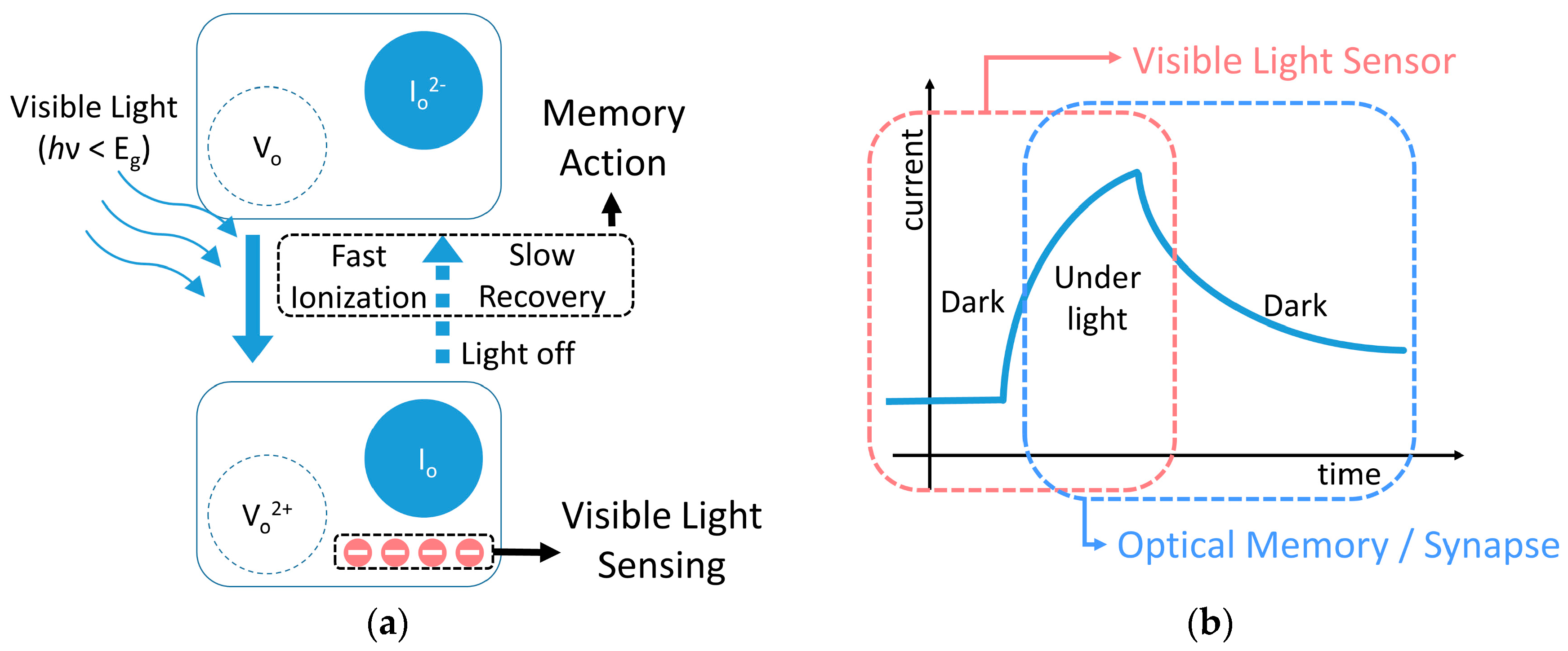
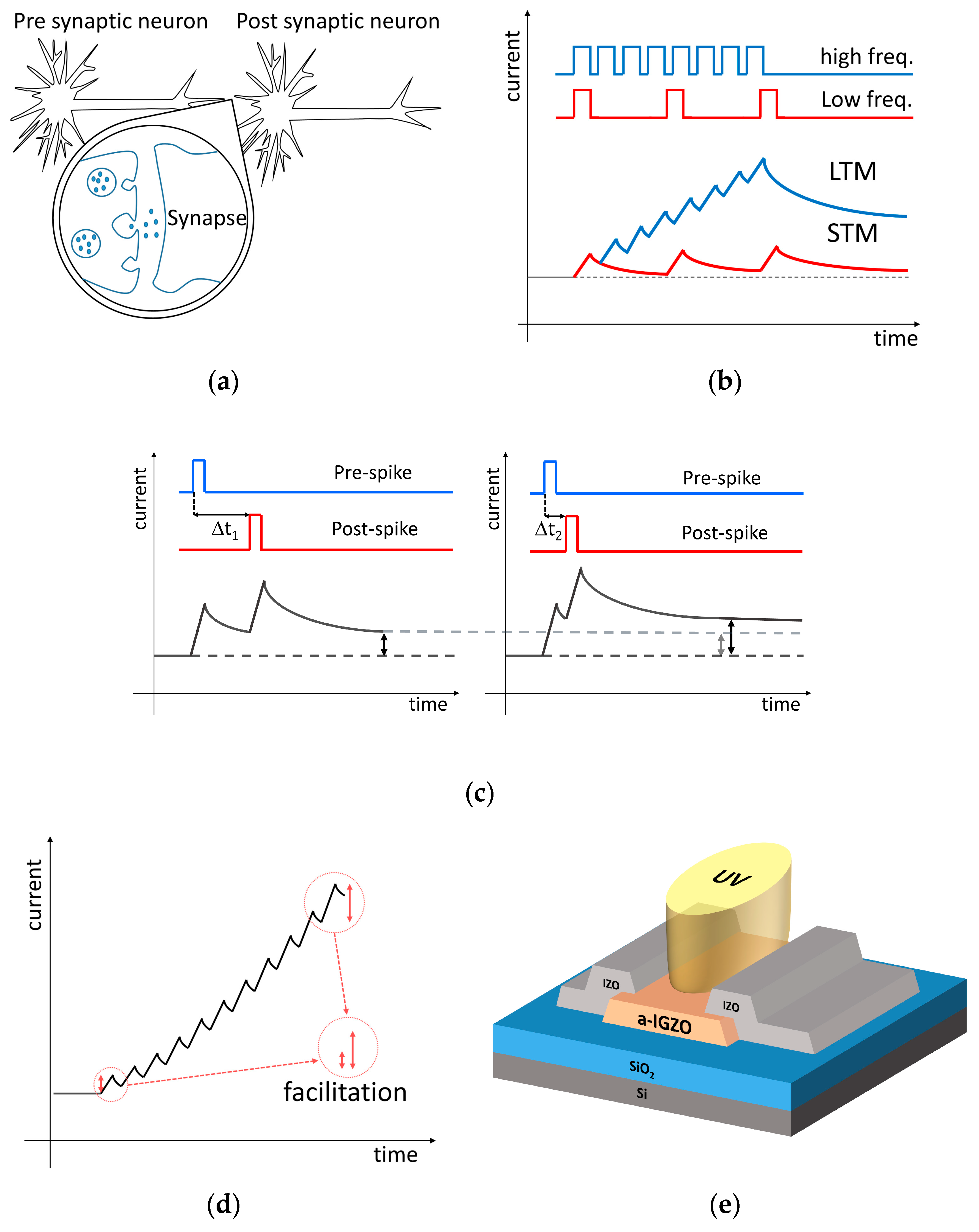
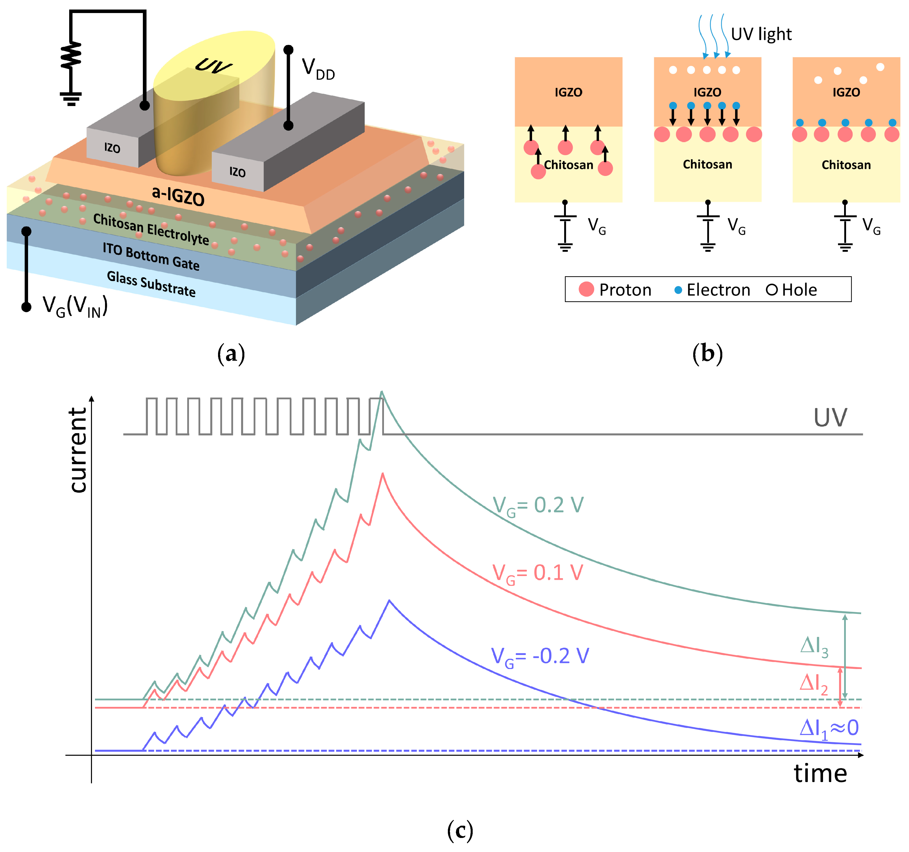
3.2. Optical Synaptic Devices with an Optical Memory-Action

Though the PPC can be problematic for sensor applications, it is a memory action naturally induced under illumination. Inspired by this aspect, there have been several reports about synaptic devices mimicking a biological synapse. There are key functions that the synaptic devices should emulate, such as a spike-timing–dependent plasticity (STDP), short-term memory (STM) to long-term memory (LTM) transition, and facilitation (Figure 6a–d). Indeed, there are other possible types for synaptic devices (e.g., resistive switching devices [48,49], atomic-switching devices [50], and transistor-based devices [51,52,53]), which use an electrical signal, as the biological synapse does. Compared to these electrical-stimulus types, TCO-based synaptic devices, which use an optical stimulus, may offer much wider bandwidth, ultrafast signal transmission, low crosstalk, and being avoided from electrical shortcoming induced by a parasitic effect like the Miller effect [26,54]. Here, an issue to be resolved is still remaining to deal with the optical stimulus and current signal in a system level.
A two-terminal synaptic device which uses the UV light pulses as the pre-synaptic stimulus has been demonstrated by Lee et al. [26]. Figure 6e shows its device structure. When the IGZO channel layer was exposed to the UV light, the drain current increased owing to the band-to-band excitation and ionization of oxygen defects at the same time. Once the UV light was turned off, current showed a slow decay due to the aforementioned PPC phenomenon. Here, it can be suggested that extra oxygen vacancies can also be created by the UV light since it is a high energy light [19,23], and these additionally contribute to the further increase and slow decay of the photocurrent. These slow decay suggests a memory action arising from the PPC, so that the device with the IGZO layer has an optical synaptic operation. In addition, the activation energy of an IGZO film increases under continuously illuminated UV pulses, incurring energy-state dependent facilitation (See Figure 6d). A slow decay of the post-illumination current and an increase of activation energy can lead to the frequency response of the photocurrent. This implies that it can also mimic timing-dependent memory actions of the brain synapse, such as the STDP and STM-LTM transition (see Figure 6b,c).
To electrically control PPC behavior for handling complex functions and distinguishable hysteresis, three-terminal devices were reported [27]. Here, the device adopted HfOx as a gate insulator in TFT, which was thought to be a defective material. The hysteresis, which was induced by trapping and de-trapping of carriers at the IGZO/HfOx interface and within the HfOx layer [55], could assist the inherent PPC perform timing-related synaptic functions (Figure 6b–d)) in the IGZO layer. In addition, when a positive voltage pulse was applied to the gate electrode, the drain current had decreased due to electrons trapped by the defects. The experimental result of the effect is conceptually schemed in Figure 7c. Here, the authors demonstrated paired-pulse depression with this operation, which mimicked the decrease of synaptic weight under pre-synaptic stimulus in the synapse.
For another type of three-terminal device, the chitosan electrolyte is incorporated between the IGZO channel layer and ITO gate layer [28], as seen in Figure 8a. Under a positive gate bias, protons will accumulate near the interface between the IGZO and chitosan-electrolyte [56], and it helps the light-induced electrons stay at the interface even longer, reinforcing the PPC behavior (see Figure 8b). In this way, the amplitude of the optical response can be controlled with modulating the gate voltage. The experimental result of this operation is shown in Figure 8c. The authors call it a depression mode to potentiation mode transition. These examples discussed here clearly confirm that the TCO-based device with the PPC optical memory phenomena can be used as an optical synaptic transistor for an advanced neuromorphic system in a novel way, where an optoelectronic operating principle is employed rather than a just electrical operation.

4. Conclusions

We have discussed physical mechanisms and derived applications of the TCO-based thin-film devices in terms of how to intentionally use their optical properties associated with oxygen defects under illumination, such as the PPC. For photo sensing applications which can detect visible lights with TFT structures, it has been found that a positive voltage pulse is required to get rid of the PPC after illumination. In other words, a fast recombination of ionized oxygen defects, i.e., metastable states, is required. At the same time, it is also important to reinforce the persistency for an optical memory, such as artificial synapses with light stimuli. From applications referred in this work, it is expected that the TCO can be used as advanced multi-functional devices, while maintaining its advantages, such as a high transparency and high electrical performance.

Author Contributions

S.L. organized this work and finalized the whole manuscript. J.J. wrote the draft of the manuscript while discussing with other authors. J.J. and Y.K. prepared and reviewed Section 3, and D.C. and J.B. did Section 2.

Funding

This research was supported in part by Samsung Electronics (201900610001) and the Basic Science Research Program through the National Research Foundation of Korea (NRF) funded by the Ministry of Science, ICT & Future Planning (NRF-2018R1C1B6001688).

Conflicts of Interest

The authors declare no conflict of interest.

References

  1. Nathan, A.; Lee, S.; Jeon, S.; Robertson, J. Amorphous Oxide Semiconductor TFTs for Displays and Imaging. J. Disp. Technol. 2014, 10, 917–927. [Google Scholar] [CrossRef]
  2. Kamiya, T.; Hosono, H. Material characteristics and applications of transparent amorphous oxide semiconductors. NPG Asia Mater. 2010, 2, 15–22. [Google Scholar] [CrossRef]
  3. Nomura, K.; Ohta, H.; Takagi, A.; Kamiya, T.; Hirano, M.; Hosono, H.J.N. Room-temperature fabrication of transparent flexible thin-film transistors using amorphous oxide semiconductors. Nature 2004, 432, 488. [Google Scholar] [CrossRef] [PubMed]
  4. Hosono, H. 68.3: Invited Paper: Transparent Amorphous Oxide Semiconductors for High Performance TFT. In Proceedings of SID Symposium Digest of Technical Papers; Blackwell Publishing Ltd.: Oxford, UK, 2007; pp. 1830–1833. [Google Scholar]
  5. Park, J.S.; Maeng, W.-J.; Kim, H.-S.; Park, J.-S. Review of recent developments in amorphous oxide semiconductor thin-film transistor devices. Thin Solid Films 2012, 520, 1679–1693. [Google Scholar] [CrossRef]
  6. Lee, S.; Jeon, S.; Chaji, R.; Nathan, A. Transparent Semiconducting Oxide Technology for Touch Free Interactive Flexible Displays. Proc. IEEE 2015, 103, 644–664. [Google Scholar]
  7. Kamiya, T.; Nomura, K.; Hosono, H. Present status of amorphous In-Ga-Zn-O thin-film transistors. Sci. Technol. Adv. Mater. 2010, 11, 044305. [Google Scholar] [CrossRef] [PubMed]
  8. Kamiya, T.; Nomura, K.; Hosono, H. Origins of High Mobility and Low Operation Voltage of Amorphous Oxide TFTs: Electronic Structure, Electron Transport, Defects and Doping. J. Disp. Technol. 2009, 5, 468–483. [Google Scholar] [CrossRef]
  9. Nathan, A.; Lee, S.; Jeon, S.; Song, I.; Chung, U.I.J.I.D. Transparent oxide semiconductors for advanced display applications. Inf. Disp. 2013, 29, 6–11. [Google Scholar] [CrossRef]
  10. Yin, H.; Kim, S.; Kim, C.J.; Song, I.; Park, J.; Kim, S.; Park, Y. Fully transparent nonvolatile memory employing amorphous oxides as charge trap and transistor’s channel layer. Appl. Phys. Lett. 2008, 93, 172109. [Google Scholar] [CrossRef]
  11. Nomura, K.; Takagi, A.; Kamiya, T.; Ohta, H.; Hirano, M.; Hosono, H. Amorphous Oxide Semiconductors for High-Performance Flexible Thin-Film Transistors. Jpn. J. Appl. Phys. 2006, 45, 4303–4308. [Google Scholar] [CrossRef]
  12. Fortunato, E.; Barquinha, P.; Martins, R. Oxide semiconductor thin-film transistors: A review of recent advances. Adv. Mater. 2012, 24, 2945–2986. [Google Scholar] [CrossRef]
  13. Nathan, A.; Lee, S.; Jeon, S.; Song, I.; Chung, U.I. 3.1: Invited Paper: Amorphous Oxide TFTs: Progress and Issues. In Proceedings of SID Symposium Digest of Technical Papers; Blackwell Publishing Ltd.: Oxford, UK, 2012; pp. 1–4. [Google Scholar]
  14. Janotti, A.; Van de Walle, C.G. Oxygen vacancies in ZnO. Appl. Phys. Lett. 2005, 87, 122102. [Google Scholar] [CrossRef]
  15. Liu, L.; Mei, Z.; Tang, A.; Azarov, A.; Kuznetsov, A.; Xue, Q.-K.; Du, X. Oxygen vacancies: The origin ofn-type conductivity in ZnO. Phys. Rev. B 2016, 93, 235305. [Google Scholar] [CrossRef]
  16. Leenheer, A.J.; Perkins, J.D.; van Hest, M.F.A.M.; Berry, J.J.; O’Hayre, R.P.; Ginley, D.S. General mobility and carrier concentration relationship in transparent amorphous indium zinc oxide films. Phys. Rev. B 2008, 77, 115215. [Google Scholar] [CrossRef]
  17. Kim, S.; Kim, S.; Kim, C.; Park, J.; Song, I.; Jeon, S.; Ahn, S.-E.; Park, J.-S.; Jeong, J.K. The influence of visible light on the gate bias instability of In–Ga–Zn–O thin film transistors. Solid-State Electron. 2011, 62, 77–81. [Google Scholar] [CrossRef]
  18. Jeon, J.-H.; Kim, J.; Ryu, M.-K. Instability of an Amorphous Indium Gallium Zinc Oxide TFT under Bias and Light Illumination. J. Korean Phys. Soc. 2011, 58, 158–162. [Google Scholar] [CrossRef]
  19. Gurwitz, R.; Cohen, R.; Shalish, I. Interaction of light with the ZnO surface: Photon induced oxygen “breathing,” oxygen vacancies, persistent photoconductivity, and persistent photovoltage. J. Appl. Phys. 2014, 115, 033701. [Google Scholar] [CrossRef]
  20. Chowdhury, M.D.H.; Migliorato, P.; Jang, J. Light induced instabilities in amorphous indium–gallium–zinc–oxide thin-film transistors. Appl. Phys. Lett. 2010, 97, 173506. [Google Scholar] [CrossRef]
  21. Lee, S.; Nathan, A.; Jeon, S.; Robertson, J. Oxygen Defect-Induced Metastability in Oxide Semiconductors Probed by Gate Pulse Spectroscopy. Sci. Rep. 2015, 5, 14902. [Google Scholar] [CrossRef]
  22. Ghaffarzadeh, K.; Nathan, A.; Robertson, J.; Kim, S.; Jeon, S.; Kim, C.; Chung, U.I.; Lee, J.-H. Persistent photoconductivity in Hf–In–Zn–O thin film transistors. Appl. Phys. Lett. 2010, 97, 143510. [Google Scholar] [CrossRef]
  23. Hensling, F.V.E.; Keeble, D.J.; Zhu, J.; Brose, S.; Xu, C.; Gunkel, F.; Danylyuk, S.; Nonnenmann, S.S.; Egger, W.; Dittmann, R. UV radiation enhanced oxygen vacancy formation caused by the PLD plasma plume. Sci. Rep. 2018, 8, 8846. [Google Scholar] [CrossRef]
  24. Takagi, A.; Nomura, K.; Ohta, H.; Yanagi, H.; Kamiya, T.; Hirano, M.; Hosono, H. Carrier transport and electronic structure in amorphous oxide semiconductor, a-InGaZnO4. Thin Solid Films 2005, 486, 38–41. [Google Scholar] [CrossRef]
  25. Jeon, S.; Ahn, S.E.; Song, I.; Kim, C.J.; Chung, U.I.; Lee, E.; Yoo, I.; Nathan, A.; Lee, S.; Robertson, J.; et al. Gated three-terminal device architecture to eliminate persistent photoconductivity in oxide semiconductor photosensor arrays. Nat. Mater. 2012, 11, 301–305. [Google Scholar] [CrossRef]
  26. Lee, M.; Lee, W.; Choi, S.; Jo, J.W.; Kim, J.; Park, S.K.; Kim, Y.H. Brain-Inspired Photonic Neuromorphic Devices using Photodynamic Amorphous Oxide Semiconductors and their Persistent Photoconductivity. Adv. Mater. 2017, 29, 1700951. [Google Scholar] [CrossRef] [PubMed]
  27. Wu, Q.; Wang, J.; Cao, J.; Lu, C.; Yang, G.; Shi, X.; Chuai, X.; Gong, Y.; Su, Y.; Zhao, Y.; et al. Photoelectric Plasticity in Oxide Thin Film Transistors with Tunable Synaptic Functions. Adv. Electron. Mater. 2018, 4, 1800556. [Google Scholar] [CrossRef]
  28. Yang, Y.; He, Y.; Nie, S.; Shi, Y.; Wan, Q. Light Stimulated IGZO-Based Electric-Double-Layer Transistors For Photoelectric Neuromorphic Devices. IEEE Electron Device Lett. 2018, 39, 897–900. [Google Scholar] [CrossRef]
  29. Facchetti, A.; Marks, T. Transparent Electronics: From Synthesis to Applications; John Wiley & Sons: Hoboken, NJ, USA, 2010. [Google Scholar]
  30. Han, W.H.; Oh, Y.J.; Chang, K.J.; Park, J.-S. Electronic Structure of Oxygen Interstitial Defects in Amorphous In-Ga-Zn-O Semiconductors and Implications for Device Behavior. Phys. Rev. Appl. 2015, 3, 044008. [Google Scholar] [CrossRef]
  31. Rhodes, C.; Franzen, S.; Maria, J.-P.; Losego, M.; Leonard, D.N.; Laughlin, B.; Duscher, G.; Weibel, S. Surface plasmon resonance in conducting metal oxides. J. Appl. Phys. 2006, 100, 054905. [Google Scholar] [CrossRef]
  32. Yu, X.; Marks, T.J.; Facchetti, A. Metal oxides for optoelectronic applications. Nat. Mater. 2016, 15, 383–396. [Google Scholar] [CrossRef]
  33. Jianke, Y.; Ningsheng, X.; Shaozhi, D.; Jun, C.; Juncong, S.; Shieh, H.D.; Po-Tsun, L.; Yi-Pai, H. Electrical and Photosensitive Characteristics of a-IGZO TFTs Related to Oxygen Vacancy. IEEE Trans. Electron Devices 2011, 58, 1121–1126. [Google Scholar] [CrossRef]
  34. Nomura, K.; Kamiya, T.; Yanagi, H.; Ikenaga, E.; Yang, K.; Kobayashi, K.; Hirano, M.; Hosono, H. Subgap states in transparent amorphous oxide semiconductor, In–Ga–Zn–O, observed by bulk sensitive x-ray photoelectron spectroscopy. Appl. Phys. Lett. 2008, 92, 202117. [Google Scholar] [CrossRef]
  35. Lee, S.; Jeon, S.; Robertson, J.; Nathan, A. How to achieve ultra high photoconductive gain for transparent oxide semiconductor image sensors. In Proceedings of the 2012 International Electron Devices Meeting, San Francisco, CA, USA, 10–13 December 2012. [Google Scholar]
  36. Janotti, A.; Van de Walle, C.G. Fundamentals of zinc oxide as a semiconductor. Rep. Prog. Phys. 2009, 72, 126501. [Google Scholar] [CrossRef]
  37. Jang, J.T.; Park, J.; Ahn, B.D.; Kim, D.M.; Choi, S.J.; Kim, H.S.; Kim, D.H. Study on the photoresponse of amorphous In-Ga-Zn-O and zinc oxynitride semiconductor devices by the extraction of sub-gap-state distribution and device simulation. ACS Appl. Mater. Interfaces 2015, 7, 15570–15577. [Google Scholar] [CrossRef]
  38. Kamiya, T.; Nomura, K.; Hirano, M.; Hosono, H. Electronic structure of oxygen deficient amorphous oxide semiconductor a-InGaZnO4-x: Optical analyses and first-principle calculations. Phys. Status Solidi (C) 2008, 5, 3098–3100. [Google Scholar] [CrossRef]
  39. Noh, H.-K.; Chang, K.J.; Ryu, B.; Lee, W.-J. Electronic structure of oxygen-vacancy defects in amorphous In-Ga-Zn-O semiconductors. Phys. Rev. B 2011, 84, 115205. [Google Scholar] [CrossRef]
  40. Chong, E.-G.; Chun, Y.-S.; Kim, S.-H.; Lee, S.-Y. Effect of oxygen on the threshold voltage of a-IGZO TFT. J. Electr. Eng. Technol. 2011, 6, 539–542. [Google Scholar] [CrossRef]
  41. Jeon, S.; Ahn, S.-E.; Song, I.; Jeon, Y.; Kim, Y.; Kim, S.; Choi, H.; Kim, H.; Lee, E.; Lee, S. Dual gate photo-thin film transistor with high photoconductive gain for high reliability, and low noise flat panel transparent imager. In Proceedings of the 2011 International Electron Devices Meeting, Washington, DC, USA, 5–7 December 2011. [Google Scholar]
  42. Ahn, S.E.; Song, I.; Jeon, S.; Jeon, Y.W.; Kim, Y.; Kim, C.; Ryu, B.; Lee, J.H.; Nathan, A.; Lee, S.; et al. Metal oxide thin film phototransistor for remote touch interactive displays. Adv. Mater. 2012, 24, 2631–2636. [Google Scholar] [CrossRef] [PubMed]
  43. Ghaffarzadeh, K.; Nathan, A.; Robertson, J.; Kim, S.; Jeon, S.; Kim, C.; Chung, U.-I.; Lee, J.H. Instability in threshold voltage and subthreshold behavior in Hf–In–Zn–O thin film transistors induced by bias-and light-stress. Appl. Phys. Lett. 2010, 97, 113504. [Google Scholar] [CrossRef]
  44. Flewitt, A.J.; Powell, M.J. A thermalization energy analysis of the threshold voltage shift in amorphous indium gallium zinc oxide thin film transistors under simultaneous negative gate bias and illumination. J. Appl. Phys. 2014, 115. [Google Scholar] [CrossRef]
  45. Jeon, S.; Song, I.; Lee, S.; Ryu, B.; Ahn, S.E.; Lee, E.; Kim, Y.; Nathan, A.; Robertson, J.; Chung, U.I. Origin of high photoconductive gain in fully transparent heterojunction nanocrystalline oxide image sensors and interconnects. Adv. Mater. 2014, 26, 7102–7109. [Google Scholar] [CrossRef] [PubMed]
  46. Lee, S.; Nathan, A.; Robertson, J. Challenges in visible wavelength detection using optically transparent oxide semiconductors. In Proceedings of the SENSORS, 2012 IEEE, Taipei, Taiwan, 28–31 October 2012; pp. 1–4. [Google Scholar]
  47. Liu, P.T.; Ruan, D.B.; Yeh, X.Y.; Chiu, Y.C.; Zheng, G.T.; Sze, S.M. Highly Responsive Blue Light Sensor with Amorphous Indium-Zinc-Oxide Thin-Film Transistor based Architecture. Sci. Rep. 2018, 8, 8153. [Google Scholar] [CrossRef] [PubMed]
  48. Shi, J.; Ha, S.D.; Zhou, Y.; Schoofs, F.; Ramanathan, S. A correlated nickelate synaptic transistor. Nat. Commun. 2013, 4, 2676. [Google Scholar] [CrossRef] [PubMed]
  49. Jiang, R.; Ma, P.; Han, Z.; Du, X. Habituation/Fatigue behavior of a synapse memristor based on IGZO-HfO2 thin film. Sci. Rep. 2017, 7, 9354. [Google Scholar] [CrossRef] [PubMed]
  50. Ohno, T.; Hasegawa, T.; Tsuruoka, T.; Terabe, K.; Gimzewski, J.K.; Aono, M. Short-term plasticity and long-term potentiation mimicked in single inorganic synapses. Nat. Mater. 2011, 10, 591–595. [Google Scholar] [CrossRef] [PubMed]
  51. Choi, H.-S.; Wee, D.-H.; Kim, H.; Kim, S.; Ryoo, K.-C.; Park, B.-G.; Kim, Y. 3-D Floating-Gate Synapse Array With Spike-Time-Dependent Plasticity. IEEE Trans. Electron Devices 2018, 65, 101–107. [Google Scholar] [CrossRef]
  52. Zhu, L.Q.; Wan, C.J.; Guo, L.Q.; Shi, Y.; Wan, Q. Artificial synapse network on inorganic proton conductor for neuromorphic systems. Nat. Commun. 2014, 5, 3158. [Google Scholar] [CrossRef] [PubMed]
  53. Gopalakrishnan, R.; Basu, A. Triplet Spike Time-Dependent Plasticity in a Floating-Gate Synapse. IEEE Trans. Neural Netw. Learn. Syst. 2017, 28, 778–790. [Google Scholar] [CrossRef]
  54. Li, H.K.; Chen, T.P.; Liu, P.; Hu, S.G.; Liu, Y.; Zhang, Q.; Lee, P.S. A light-stimulated synaptic transistor with synaptic plasticity and memory functions based on InGaZnOx–Al2O3 thin film structure. J. Appl. Phys. 2016, 119, 244505. [Google Scholar] [CrossRef]
  55. Zhu, W.J.; Ma, T.P.; Zafar, S.; Tamagawa, T. Charge trapping in ultrathin hafnium oxide. IEEE Electron Device Lett. 2002, 23, 597–599. [Google Scholar] [CrossRef]
  56. Du, H.; Lin, X.; Xu, Z.; Chu, D. Electric double-layer transistors: A review of recent progress. J. Mater. Sci. 2015, 50, 5641–5673. [Google Scholar] [CrossRef]
Figure 1. Optical transmission spectrum of the a-IGZO device for two different concentrations. A dashed line is ne ~ 1013/cm3 and a solid line is ne ~ 1020/cm3. Here, significant decrease of the transmittance of long wavelength light is found for the higher carrier concentration case (redrawn and adapted from [24]).
Crystals 09 00192 g001
Figure 2. (a) Comparative Tauc plot for each carrier concentration (ne ~ 1013/cm3 and ne ~ 1020/cm3). (b) Conceptual Tauc plots to compare two different cases – large and small (IZO/IGZO) amount of oxygen defects (redrawn and adapted from [6]).
Crystals 09 00192 g002
Figure 3. (a) Reaction diagram about ionizations of oxygen defects under illumination. Here, the lattice of the oxygen vacancy is depicted to be relaxed during the optically-induced ionization, thus an increase of the activation energy (redrawn and adapted from [21]). (b) Conductivity as a function of time. A seen, under illumination, conductivity of the transparent conducting oxide (TCO) film increases due to emitted free electrons during ionization process of the oxygen defects, and that under dark slowly decreases due to slow recombination of the free electrons.
Crystals 09 00192 g003
Figure 4. (a) Conceptual diagram to describe an optical memory-action and light-reactivity through the ionization of oxygen defects. (b) Indication of functional regions of the current as a function of time for each device.
Crystals 09 00192 g004
Figure 5. (a) Conceptual plot of the drain current of the TCO-based optical device. Here, the positive gate pulse makes dark signal level after illumination as same as the level before illumination as illustrated in this figure. (b) Energy band diagram of the device when positive gate pulse is applied. Here, it is described that the increased electron concentration of the film accelerates deionization of the oxygen defect (redrawn and adopted from [25]).
Crystals 09 00192 g005
Figure 6. (a) Schematic showing neurons and synapses. (b) Frequency dependent short-term memory (STM) and long-term memory (LTM). (c) Plasticity variation with spike timing interval, spike-timing–dependent plasticity (STDP). (d) Facilitation under periodic pulses. (e) Device structure (redrawn and adopted from [26]).
Crystals 09 00192 g006
Figure 7. (a) Device structure. (b) Conceptual diagram of device operating under light pulse (left) and electrical pulse (right) applied. (c) Experimental result from the device operating under electrical pulses. With a short enough interval time between two pulses (Δt1), drain current is decreased due to the trapped electrons in the HfOx layer. On the other hand, with the long enough interval (Δt2), the current level recovers from the depression effect (redrawn and adopted from [27]).
Crystals 09 00192 g007
Figure 8. (a) Device structure and operating circuit. (b) Conceptual diagram of proton migration under gate bias and UV light illumination. (c) Experimental result from the device operating under different gate biases. The current differences ΔI1, ΔI2, and ΔI3 mimic the variation of synaptic weight depending on the gate bias (redrawn and adopted from [28]).
Crystals 09 00192 g008

