1. Introduction
The solar absorption films coated on the solar receiver of solar thermal electricity Stirling engine [
1] can increase the absorption of sunlight. A method to increase the absorption of sunlight in the film is to develop a textured surface on the film [
2]. This effectively increases solar absorption by trapping sunlight in the textured structure and transfer heat to the solar receiver. Additionally, the textured structure is simple and easy to fabricate. In this work, nano-porous structures have been used as the main basis of the textured structure of the absorption film. This textures structure has been previously used to reduce the reflectivity on solar cells to increase its efficiency [
3,
4]. A simple method to deposit the absorption film on the surface of the solar receiver of the Stirling engine is coated with a thin hydrogenated amorphous silicon (a-Si:H) film by plasma-enhanced chemical vapor deposition (PECVD) and the a-Si:H films were crystallized to polysilicon (poly-Si) film by high-temperature annealing.
There are two typical methods for wet etching to produce the texture structure on the surface of poly-Si. In our previous work [
5], potassium hydroxide (KOH) had been used to form the nano-porous structure. However, it was found that on increasing the etching time, the width of the pore also increased along with the depth. This is due to isotropic etching by KOH. The control of morphology of texture structure is limited by this isotropic etching. Another facile method to control the morphology of texture structure on the surface of Si materials is metal-assisted chemical etching (MaCE) [
6,
7]. The nanowires or micropillars [
8], vertical trenches [
9], or via array structures [
10,
11] can be obtained by controlling the size and the distribution of metal catalyzed particles or films, and the concentration of oxidants (typically hydrogen peroxide, H
2O
2) and hydrofluoric acid (HF). The metal catalyst is a micro-cathode, which reduces H
2O
2 on the metal catalyst surface into H
2O and holes that are generated in the metal catalyst. The generated holes inject from metal catalyst into Si, which induce the dissolution of Si volumes surrounding metal catalyst by HF [
6,
7,
9,
10]. The MaCE process incudes two mechanisms of the mass transport (MT) of reactants and products, and the charge transport (CT) of generation and recombination of holes [
9,
10]. The geometry of metal catalyst controls MT, while the concentration of H
2O
2 and HF dominates CT [
9,
10]. Large size metal catalyst limits the reaction near the center of metal/Si interface. Low concentration of reactants reduces the dissociation of Si volumes. The morphology of MaCE etched structure can be well controlled by tuning MT and CT processes.
The control of the morphology of MaCE etched structure also depends on the crystal structure of the Si substrate. For single crystal silicon (c-Si), the etching direction is dominantly along <100> [
8]. Vertical etching is more easily obtained for (100) silicon substrate by MaCE. The vertical etching for (110) and (111) Si can be conducted by an Au mesh with large hole spacing [
8]. For poly-Si, the different sizes and crystal orientations of grains and the grain boundaries conducts the irregular movement of metal catalyst, which results in non-uniform etching. Recently, a self-anchored catalyst (SAC) MaCE method was successfully used to fabricate the ordered vertical via array for poly-Si [
11]. The nano-porous catalyst film with pinholes produces the nanowires through pinholes. These nanowires anchor the catalyst film from detouring as it descends [
11]. The vertical etching of poly-Si can be controlled by Au mesh with large hole spacing [
8] or SAC-MaCE [
11]. The design of mesh size and hole spacing of Au mesh or the via, pitch, and pinhole size of SAC shall be considered the grain size of poly-Si.
In this work, the nano-porous poly-Si absorption film is designed for coating on the surface of stainless steel solar receiver of the Stirling engine to enhance the absorption of sun light. The poly-Si films were obtained from the high-temperature annealing of PECVD deposited a-Si:H films. These poly-Si films contain many tiny grains of average size about 30~40 nm. Unlike the previous works [
8,
11], the poly-Si films were deposited by high-temperature low-pressure chemical vapor deposition (LPCVD), for which the typical grain size is larger than 200 nm. The grain size of our poly-Si films is less than one-order of magnitude. The silver nano-particles (Ag-NPS) are used as the metal catalysts [
12,
13,
14]. The size and distribution of Ag-NPS was controlled by the thickness and very low deposition rate of thermal evaporation. The discrete Ag-NPS with small size (~19 nm), small particle-to-particle distance (~8 nm), and ~44% Ag-NPS cover area ratio (or 56% pore ratio) was used to etch the poly-Si films. The nano-porous structure was developed on the poly-Si film by Ag-NPS etching in H
2O
2 + HF + H
2O solution. The morphology of nano-porous structure was controlled by the etching time. The structural change of the obtained nano-porous structures were evaluated by surface and cross-section morphology measurements. The corresponding change of reflectance and absorbance of the films due to variation of structural change were identified.
2. Materials and Methods
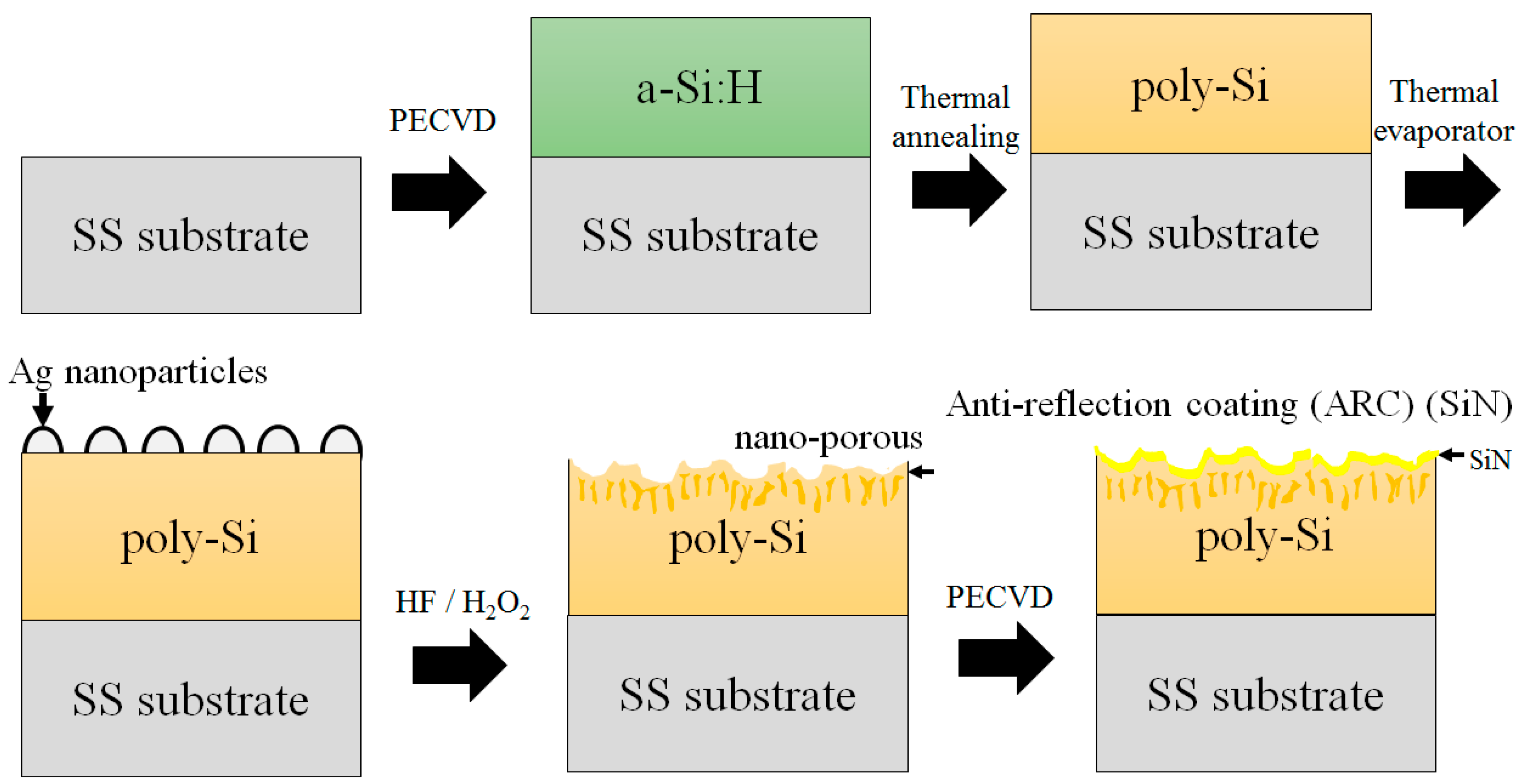
Figure 1 shows the fabrication steps as follows: (1) an a-Si:H film with a thickness of 3 μm was deposited on stainless steel (SS) substrate by using PECVD. The process conditions include SiH
4 (flow rate of 20 sccm) and H
2 flow rate (flow rate of 50 sccm), chamber pressure (0.7 torr), RF power (20 W), and substrate temperature 210 °C; (2) The a-Si:H film was annealed at a high temperature (800 °C) furnace and the furnace tube was filled with nitrogen to convert the a-Si:H film to poly-Si film; (3) The Ag-NPS layers were deposited on the surface of the poly-Si film of 2, 3, and 4 nm thickness while using thermal evaporation with a very low deposition rate of 0.4 nm/min; and, (4) The poly-Si films were etched to form nano-porous poly-Si structures by the volume ratio of H
2O
2 (31%):HF (49%):H
2O = 15 mL:5 mL:480 mL solution at room temperature. The molar concentration of H
2O
2 [M], HF [M], and H
2O [M] is 0.30 M, 0.28 M, and 53 M, respectively. The Ag-NPS was not etched after etching; (5) The nano-porous poly-Si films were coated with 75 nm thickness a-SiN
x:H film by PECVD as the antireflection and protection layer. The molar concentration ratio H
2O
2 of the HF and H
2O
2 was evaluated by Equation (1) [
11], which was 0.52.
The deposition rate of a-Si:H film was calculated by deposited a-Si:H film on glass substrate and the thickness of a-Si:H film was measured by a spectroscopic ellipsometer (J.A. Woollam M-2000, Lincoln, USA). The crystalline structures of the poly-Si films were investigated while using an X-ray spectrometer (PANalytical X’Pert PRO MRD, Almelo, Netherlands). The X-ray source was a Cu Kα radiation (λ = 0.154 nm) with acceleration voltage 45 kV and current of 40 mA, and 2°/min 2
θ scan from 20 to 60°. The grain size (
D) was evaluated by Scherrer’s Equation (2),
where,
k is a constant (
k = 0.89),
B is the full width at half maximum (FWHM) of (111) peak
λ is the X-ray wavelength (0.154 nm), and 2
θ is diffraction angle of (111) peak (28.48°).
The surface morphology of the poly-Si films and the cross-section profile were determined by a scanning electron microscopy (SEM, JEOL-6500F, JEOL Ltd., Tokyo, Japan) and a transmission electron microscopy (TEM, FEI Talos F200X, Oregon, USA). The reflectance of the films was measured by a UV-VIS/NIR spectrophotometer (JASCO V-760, Tokyo, Japan) with the integrating sphere and the scan range from 250 nm to 2500 nm. The absorbance (
α) of the film can be calculated by Equation (3) [
15],
where, the
Isol (λ) is the solar AM1.5 spectrum.
3. Results and Discussion
The a-Si:H film was annealed at a high temperature furnace (800 °C) and the furnace tube was filled with nitrogen and was heated at a rate of 5 °C/min. After every increase of 100 °C, the temperature was maintained for 1 h, and at the temperatures of 375 °C and 475 °C, the temperature was maintained for 2 h, since hydrogen is released from the film. This process was continued until the temperature reached 800 °C, after which the temperature was held for 12 h. Following this procedure, the film was annealed into a polycrystalline silicon thin film.
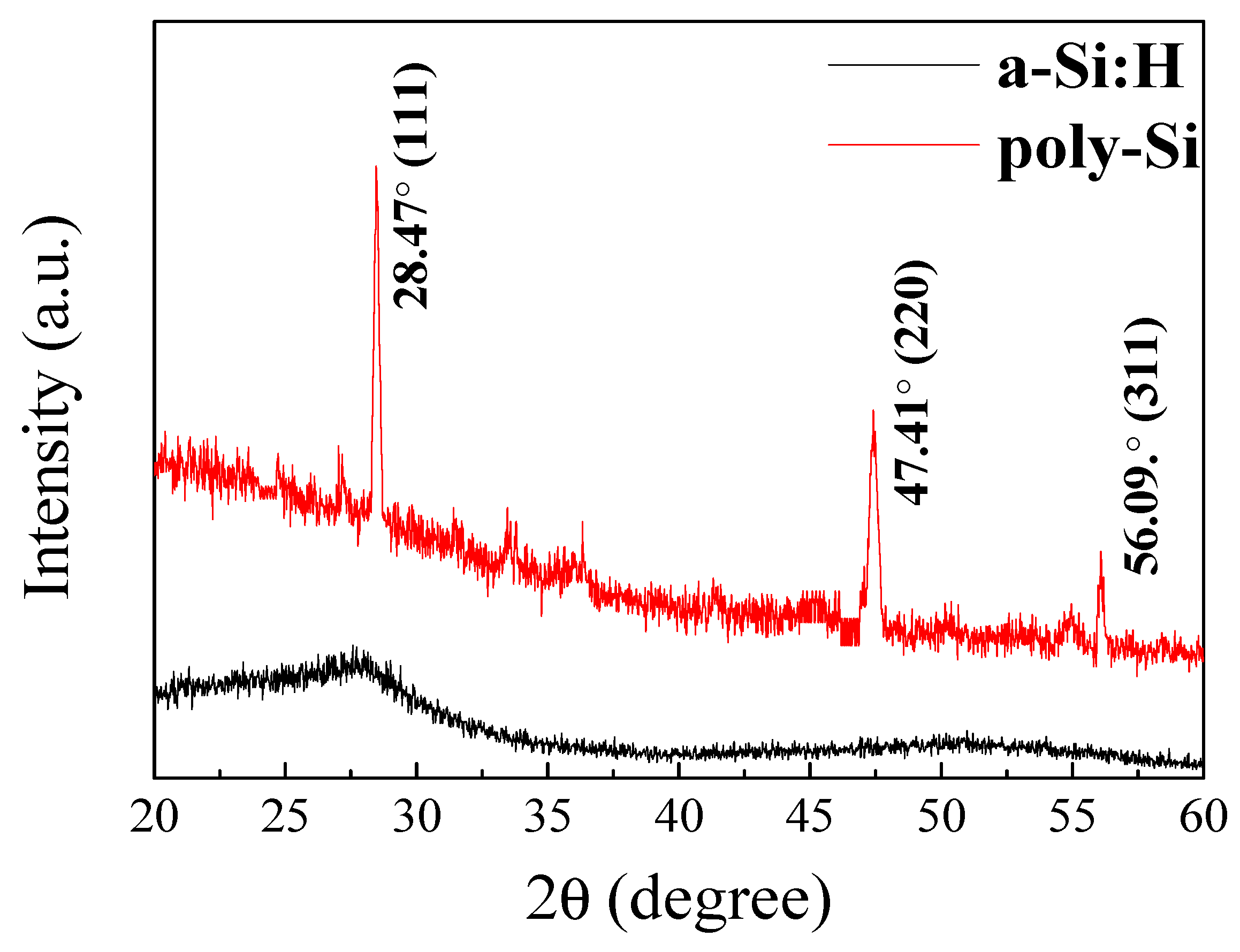
Figure 2 shows the
θ–2
θ diffraction patterns of these poly-Si films. The 2
θ of 28.47°, 47.41°, and 56.09° corresponds to Si (111), (220), and (311) crystalline peaks. Successfully converting the film transform to poly-Si.
Table 1 summarizes the peak intensity and the full width at half maximum (FWHM:
B) of (111) peak, and the grain size (
D) of the poly-Si films. The typical grain size is the value of approximately 32 nm. The crystal structure of the poly-Si films is a mixed structure of many tiny grains. Comparison with the grain size larger than 200 nm of poly-Si films deposited by high-temperature LPCVD [
11], there are many grain boundaries between tiny grains of our poly-Si films. The dissociation of Si atoms in grain boundaries is much easier and faster than the atoms in grains. The MaCE occurs more readily at the grain boundaries [
11]. The detouring of metal catalyst around gains is more severely in poly-Si films with tiny grains.
Many researchers prepare Ag-NPS by liquid chemical deposition process. The uniform distribution of different size of Ag-NPS can be obtained [
12]. Another easy deposition method is physical evaporation. Discrete or continuous distribution of metal catalyst can be controlled by change the thickness and the deposition rate of an e-beam evaporation [
10,
11]. In this work, we used the simple physical thermal evaporation to deposit the discrete and uniform distribution Ag-NPS on the surface of the poly-Si films. The size and the density of Ag-NPS could be easily obtained by only change the deposition time of very slow deposition rate of thermal evaporation. The Ag-NPS were deposited on the surface of the poly-Si film by a thermal evaporator with a very low deposition rate of about 0.4 nm/min.
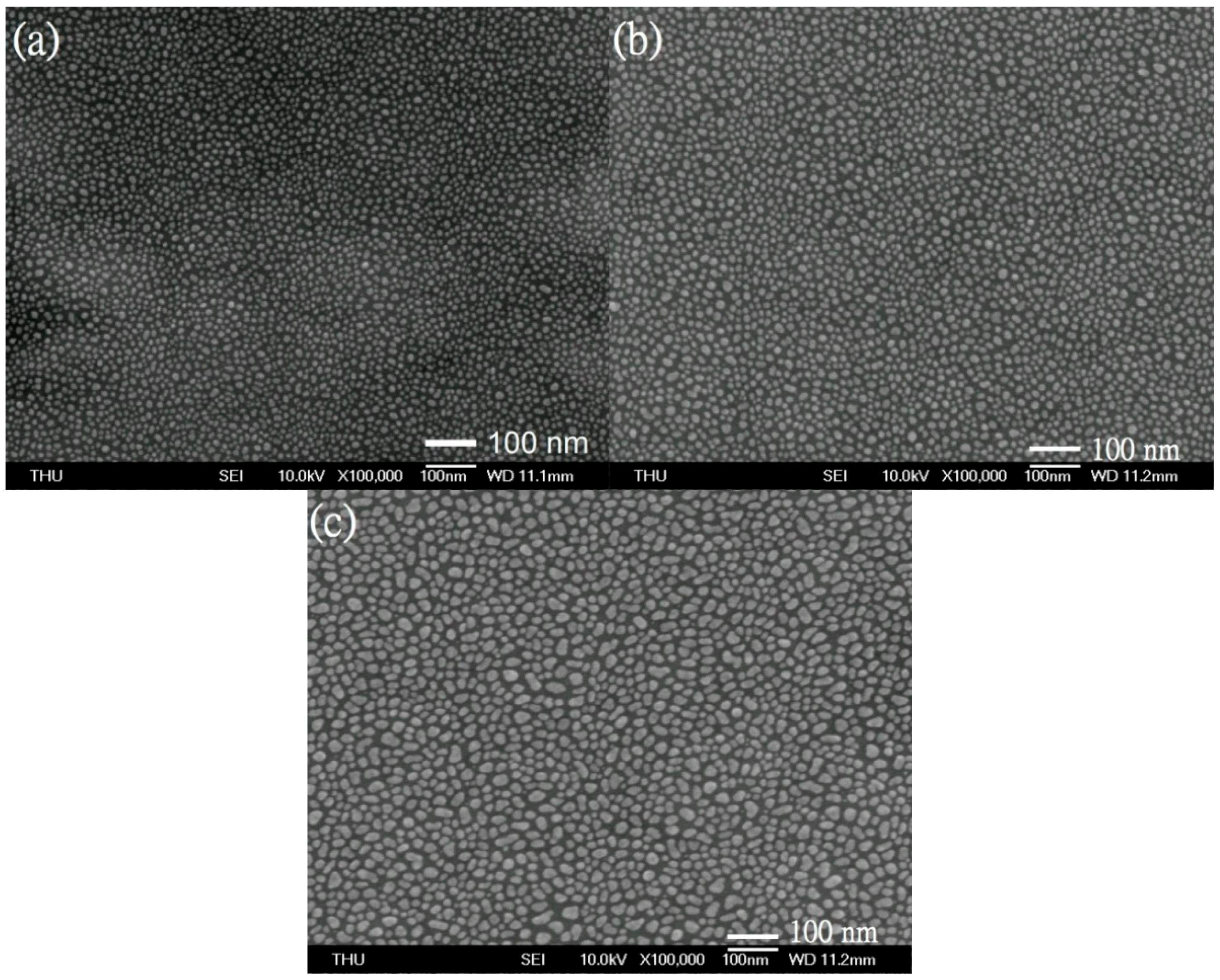
Figure 3 shows that, in case of an extremely thin silver layer, being characterized by low deposition time, the film is not continuous, but rather separated into isolated nano-sized particles, so it is called a Ag-NPS layer.
Simulation and calculation of Ag-NPS size was done with Image_J software [
16].
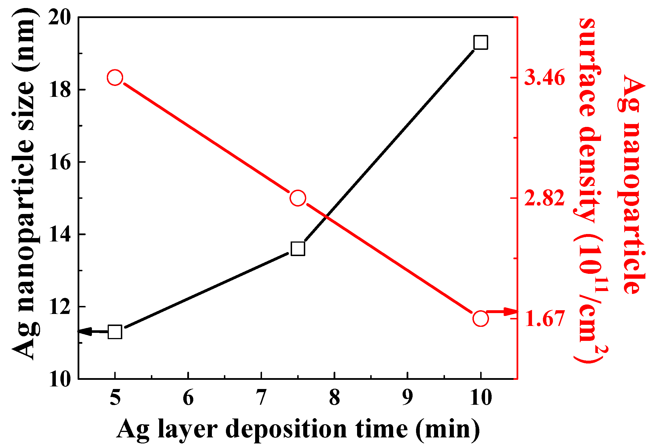
Figure 3a–c shows the Ag-NPS layer of 2, 3, and 4 nm thickness for deposition times of 5 min, 7.5 min, and 10 min, respectively. It can be seen clearly that the Ag-NPS size increases with longer deposition time, and the particle surface density reduces, in the Ag-NPS layer.
Figure 4 shows the average Ag-NPS size and surface density with respect to the Ag deposition time. The Ag-NPS diameter are 11.3 nm, 13.6 nm, and 19.3 nm, respectively. The surface densities are 3.46 × 10
11/cm
2, 2.82 × 10
11/cm
2, 1.67 × 10
11/cm
2 for the three deposition times. These results show that the size of the Ag-NPS can be controlled by the thin thickness of thermal deposition with very low deposition rate. Longer deposition time results in deposition of larger sized Ag-NPS with lower surface density. The 4 nm thickness Ag-NPS layer has particle size ~19 nm (estimating by a circular dot), the average Ag-NPS coverage ratio of 44% and surface density of 1.67 × 10
11/cm
2, corresponding to deposition time of 10 min, was chosen, for the fabrication of nano-porous poly-Si absorption films. The average Ag pore size (Ag particle-to-particle spacing) is around 8 nm and the average pore coverage ratio is approximately 56%. The geometrical relation of Ag-NPS with the grain size of poly-Si is that 19 nm Ag-NPS with 8 nm pore size distributed on the 32 nm grain size poly-Si film. Typically, one small 19 nm Ag-NPS on one tiny 32 nm crystal grain. Different from the work of Kim et al. [
11], the 6 nm thickness Au catalyst film deposited by 0.7 A/s deposition rate. The 200 nm to 900 nm Au catalyst dot with the pore size around 12 nm (area of 120 nm
2) and the average pore coverage ratio of 15% was deposited on ~200 to 300 nm crystal grain [
11]. The size of the discrete Au catalyst segment (or particle) in the dot is much smaller than the size of crystal grain. In this case, one small Au catalyst segment is located on one relative large crystal grain. The MaCE behaviors like the case of etching in c-Si. For our case, one small 19 nm Ag-NPS located on one tiny 32 nm grain, the detouring of Ag-NPS catalyst around gains will readily happen. The irregular but random nano-porous poly-Si structure will be obtained by this etching.
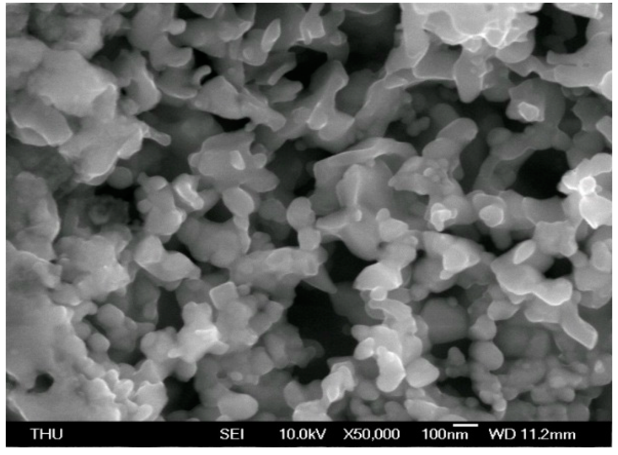
Figure 5 shows a SEM plane view of the nano-porous poly-Si film etched by Ag-NPS MaCE in H
2O
2 (31 %):HF (49 %):H
2O = 15 mL:5 mL:480 mL solution at room temperature for 1500 s. The molar concentration of H
2O
2 [M], HF [M], and H
2O [M] is 0.30 M, 0.28 M, and 53 M, respectively. The irregular nano-porous texture surface was obtained by Ag-NPS induced etching. The formation of the nano-porous texture surface is due to the small Ag-NPS detouring etching around the grain boundaries of the randomly distributed tiny crystal grains. The small discrete metal catalyst could easily etch the Si substrate to form random distribution porous structure [
11]. The small size of Ag-NPS on the same order small size of tiny grain could not produce the nano-wire to anchor or constrain the detouring movement of the Ag-NPS along the grain boundaries [
8,
10,
11]. The many different crystal directions of tiny grains also conduct the detouring etching [
11].
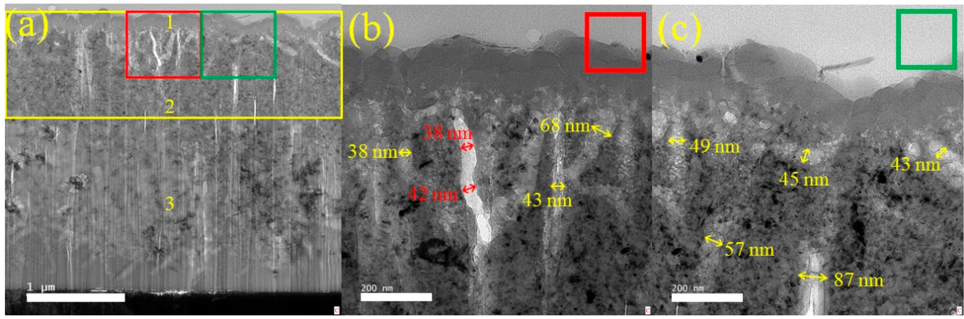
Figure 6 shows the TEM cross-section images of the nano-porous poly-Si film after 1500 s Ag-NPS MaCE.
Figure 6a shows the entire cross-section of the film. The three regions (1), (2), and (3) depicted in
Figure 6a represent the surface, thread-like pores etched region and the rest of the bulk region, respectively. The thicknesses of the texture surface region (1), thread-like pores etched region (2), and the rest of the bulk region (3) were 123 nm, 987 nm, and 1887 nm, respectively. The total thickness of the film is around 3000 nm. The region enclosed in the yellow box shows the etched region (a combination of regions (1) & (2)) with thickness 1110 nm.
Figure 6b,c shows two magnified images of two 800 nm patches in region (2). These images show the nano-porous surface texture structure in region (1) and the different thread-like pores structures etched from the surface deep into the region (2) of the poly-Si film. The widths of these threads are in the range 35–90 nm with an average width of around 54 nm. The thread-like pores structures formed due to etching have curved contours since etching follows the grain boundaries, which are not straight at all. These threads appear brighter than their surroundings. Some threads appear dimmer than the others. This is because these threads are not on this cross-section surface, but behind it, but these are projected onto the same plane. Hence, it appears as if these are all on the same cross-section surface. The bright thread marked with red in
Figure 6b is ambiguous in nature, because it cannot be ascertained whether it is an etched structure or a physical rupture. It is too bright to be considered as an etched structure, since the brightness means that it is really deep (as we look into the paper, not top to bottom). However, its width is also in the range 35–90 nm, and it has a curved contour. There are around nine roughly visible threads in each patch of 800 nm, as shown in
Figure 6b,c.
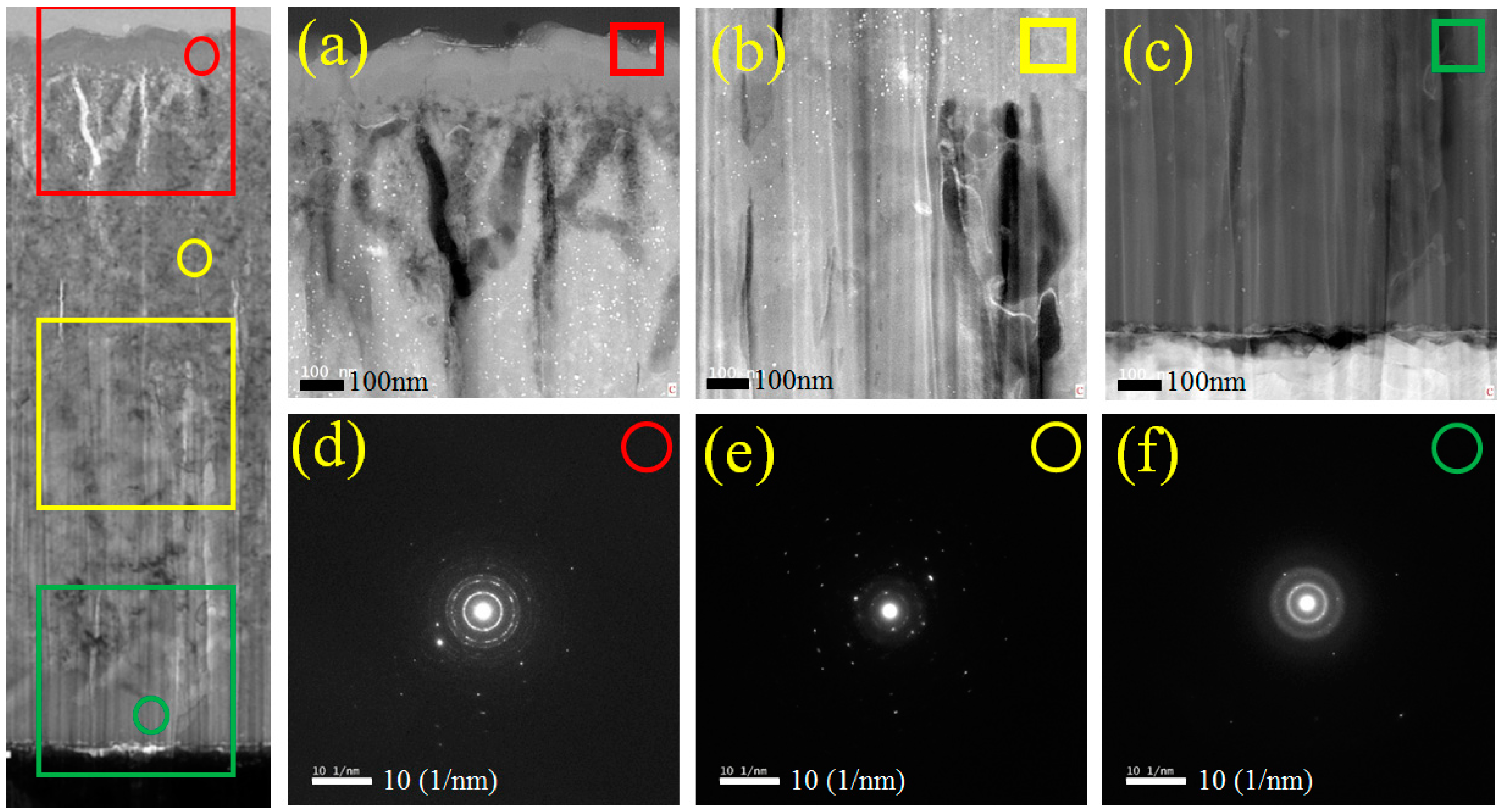
Figure 7 shows the high angle annular dark field (HAADF) and the selected area diffraction (SAD) images of three different regions (from top to bottom) of the film cross-section after 1500 s Ag-NPS induced etching. The HAADF images show enlarged versions of three regions (from top to bottom): (a) red, (b) yellow, and (c) green. The red region (
Figure 7a) is the connection region between regions (1) and (2), as shown in
Figure 6a. The yellow region (
Figure 7b) is the connection region between regions (2) and (3). Lastly, the green region (
Figure 7c) shows the connection region between (3) and the SS substrate. The red region contains a lot of thread-like pores structures with high Ag-NPS distribution. The yellow region contains lesser thread-like pores structures with lower Ag-NPS distribution. Finally, the green region contains only a few thread like structures with really low Ag-NPS distribution. It can be clearly seen from the HAADF images that the etched structure is mostly constrained to the red and upper yellow region. The rest of the depth of the film (green region) remains mostly unaffected. The SAD image for the red circle has three bright rings around the central dot. These rings correspond to the three crystalline regions (111), (220), and (311) (inner to outer), respectively. These rings are distinct in the red circle since most of the grain boundaries have been etched away, and the film shows highly crystalline behavior. For the yellow circle, the SAD image has fewer distinct rings, and the outermost ring corresponding to (311) has faded away. For the green region, the SAD image has blur rings, which indicates that there is very weak crystallinity in this region. This evidence further proves that the crystallinity of the film reduces from top to the bottom of the cross-section. The etching of grain bondaries is gradually reduced as the Ag-NPS moving deep inside the film. The possible reasion is the supply of the etchants and products are difficult through the distored thread-like pores structures. The etching ability is gradually reduced.
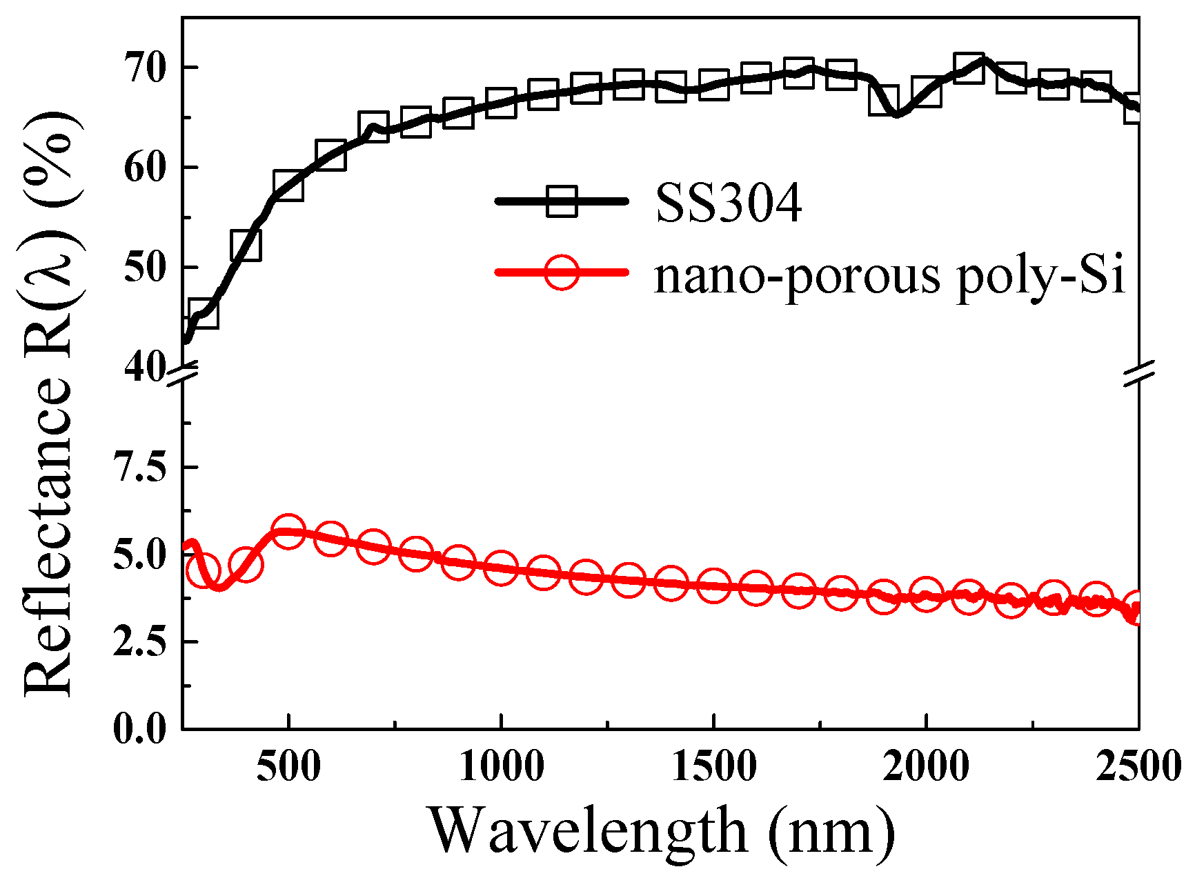
Figure 8 displays the reflectance of the reference SS substrate and the nano-porous poly-Si film on the SS substrate. In order to correct measurement of the possible diffusion light by texture structure, the reflectance is measured by a UV-VIS/NIR spectrophotometer with the integrating spheres to collect the diffusion of reflection light. The scan range is from UV, visible to near infrared light of 250 nm to 2500 nm. The reflectance of the reference SS substrate is much higher than that of the sample with the nano-porous poly-Si film. The average reflectance of the reference SS substrate and the nano-porous poly-Si sample is 65% and 4.3%, respectively. High reflectance of metal material cannot efficiently absorb the sunlight. The nano-porous poly-Si structure and the SiN
x antireflection coating enhance light trapping in the Si material, resulting in the effective reducing the reflectance. Texture structures are also applied in order to reduce the reflectance of the solar cells [
3,
4]. Very low reflectance of 1.4% in the 300 nm to 1200 nm wavelength region can be obtained by a pyramid texture structure combined with a hierarchical texture structure etched by Au nano-particles (Au-NPS) [
4]. The hierarchical texture structure by Au-NPS MaCE can further reduce reflectance. However, this novel structure needs two wet etching processes. The control of Au-NPS uniformly distributed on the surface of the pyramid texture structure is difficult.
The absorbance (α) of the reference SS sample is around 37%. The increase of light trapping in the nano-porous poly-Si sample largely increase the absorbance to 95%. The small discrete Ag-NPS on the tiny grains induced detouring etching around grain boundaries produce irregular random nano-porous structure poly-Si films on the SS substrate. It could be applied to improve the sun light absorption of the solar receiver of the solar thermal electricity Stirling Engine to enhance the efficiency.


