Article

Design and Study of Composite Film Preparation Platform

1
College of Mechanical Engineering, Hangzhou Dianzi University, Hangzhou 310018, China
2
Anji Intelligent Manufacturing Technology Research Institute Co., Ltd., Hangzhou Dianzi University, Huzhou 313000, China
3
Sanmen Sanyou Technology, Inc., Taizhou 317103, China
4
Changzhou Slav Intelligent Equipment Technology Co., Ltd., Changzhou 213162, China
*
Author to whom correspondence should be addressed.
Crystals 2024, 14(5), 389; https://doi.org/10.3390/cryst14050389
Submission received: 3 April 2024 / Revised: 17 April 2024 / Accepted: 18 April 2024 / Published: 23 April 2024

Abstract

:
This study aims to develop equipment for the preparation of composite films and successfully implement a film thickness prediction function. During the research process, we segmented the mechanical structure of the composite thin film preparation equipment into distinct modules, completed the structural design of the core module, and validated the stability of the process chamber, as well as the reasonableness of the strength and stiffness through simulation. Additionally, we devised a regression model for predicting the film thickness of composite films. The input features for the model included the sputtering air pressure, sputtering current, and sputtering time for magnetron sputtering process samples, as well as the evaporation volume and evaporation current for vacuum evaporation process samples. Simultaneously, the output features were the film thickness for both process samples. Subsequently, we established the designed composite film preparation equipment and conducted experimental verification. During the experiments, we successfully prepared Cr-Al composite films and utilized AFM for surface morphology analysis. The results confirmed the excellent performance of the Cr-Al composite films produced by the equipment, demonstrating the reliability of the equipment.

1. Introduction

Composite films, comprising alternating layers of materials with outstanding properties, find widespread applications in various fields. The intricate preparation process demands efficient, stable, controllable equipment and precise film thickness control, posing a crucial challenge in composite film production [1,2].
Cr-Al composite film is a multifunctional material with wide and diverse applications. These films play an important role in the following fields. (1) Solar cell technology: Cr-Al composite films are used as the back passivation layer of solar cells to improve the conversion efficiency of the battery; (2) high-barrier packaging: these films are used in food and medicine and high-barrier packaging of electronic products, extending product life and improving food safety; (3) mechanical engineering: Cr-Al composite films are widely used in tools, molds, and mechanical parts due to their high strength, hardness, and wear resistance; (4) medical devices, optical films, and flat panel displays: these films are also used in other areas such as medical devices, optical coatings, and flat panel displays.
Amidst the rapid advancements in science and technology [3,4,5], the current design status and developmental trends of composite thin film preparation platforms have garnered significant attention [6,7,8]. In 2023, a foreign research team devised an integrated ultrahigh-vacuum cluster system to address interfacial spin effects in spintronic multilayer films [9,10]. Simultaneously, a Japanese research team proposed a gas-injected pulsed plasma CVD method utilizing a single plasma source as an ultra-plasma deposition technique for preparing DLC films with a nanoindentation hardness of 17.5 GPa. During the same period, Antonio A. A. Chepluki, Tiago E. A. Frizon, and others developed a low-cost spin-coater for thin film deposition, serving as a cost-effective alternative to high-priced commercial equipment [11,12,13,14,15].
This research delves into the intricacies of integrating and optimizing composite thin film preparation platforms [16]. By consolidating the preparation processes of magnetron sputtering and vacuum evaporation within the same vacuum cavity, the creation of composite films tailored to the requirements of diverse high-tech fields on a single substrate is achieved [17]. Furthermore, an integrated learning algorithm is introduced for film thickness prediction, facilitating accurate forecasts for the film thickness of composite films [18,19,20]. Finally, the paper substantiates the performance and feasibility of the equipment by preparing Cr-Al composite films on PET substrate. These innovative optimizations present an effective solution to the design and prediction challenges faced by hybrid film preparation systems [21,22,23].

2. Materials and Methods

2.1. Hardware Design

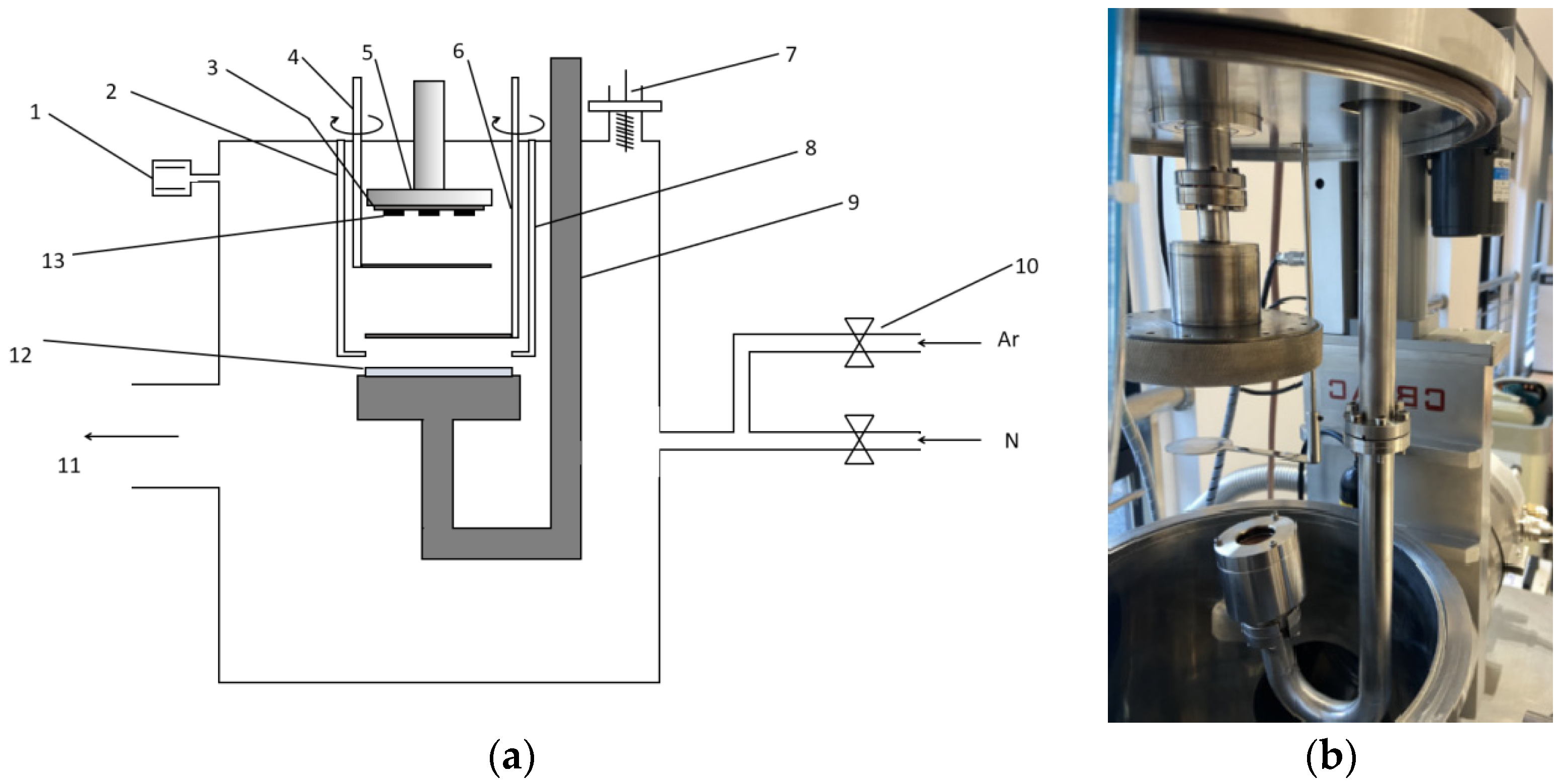
2.1.1. Overall Design

The mechanical structure design of the composite film preparation equipment outlined in this paper primarily encompasses a vacuum system capable of achieving a vacuum, a vacuum chamber creating a vacuum test environment, a process system integrating a magnetron sputtering system and a vacuum evaporation system, a transmission system responsible for opening and closing the vacuum chamber, and a cooling system for temperature control [24]. Combining the aforementioned analysis and the composition of each design component, the definitive overall structure of the composite film preparation equipment was established [25,26]. The comprehensive assembly diagram of the mechanical approach for the hybrid film preparation equipment is illustrated in Figure 1.

2.1.2. Magnetron Sputtering Module Design

The sputtering system is primarily composed of a sputtering chamber, magnetron sputtering target, sample stage, sputtering target head baffle, sample stage baffle, target head holder, and other structures [27,28,29]. The structural schematic sketch and physical drawings are presented in Figure 2a and Figure 2b, respectively.

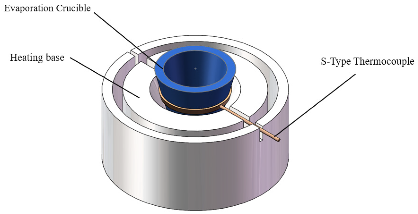
2.1.3. Evaporation System Module Design

The vacuum evaporation module stands as a pivotal component of this preparation platform, harmoniously integrated with the magnetron sputtering module to form the composite film preparation platform’s comprehensive process. The evaporation system comprises the process chamber, evaporation crucible, water-cooled pipeline, heating platform, heat source bellows, heat transfer components, and other integral elements. The structural schematic principle is illustrated in Figure 3 below.
Within the evaporation system, the evaporation crucible assumes a central role, necessitating a thorough analysis of material selection and structural design. Considering that vacuum evaporation plating employs metal and organic molecular materials, operates within a temperature range of 200 to 1300 °C, and requires efficient cooling, alumina is chosen as the primary material for the evaporation crucible. Based on the relevant literature and information, the standardized specifications for the universal evaporation crucible in vacuum evaporation plating are an outer diameter of 19.6 mm, inner diameter of 15.4 mm, and height of 24 mm. A tungsten filament serves as the heat source, with the thermocouple positioned at the crucible’s bottom for convenient temperature measurement and control. Standard configurations incorporate S-type thermocouples, and the evaporation working temperature range spans 200–1300 °C. The distance between the evaporation module and the sample stage is 60 mm. The schematic structure of the evaporation crucible is depicted in Figure 4 below, and the physical representation is presented in Figure 5.

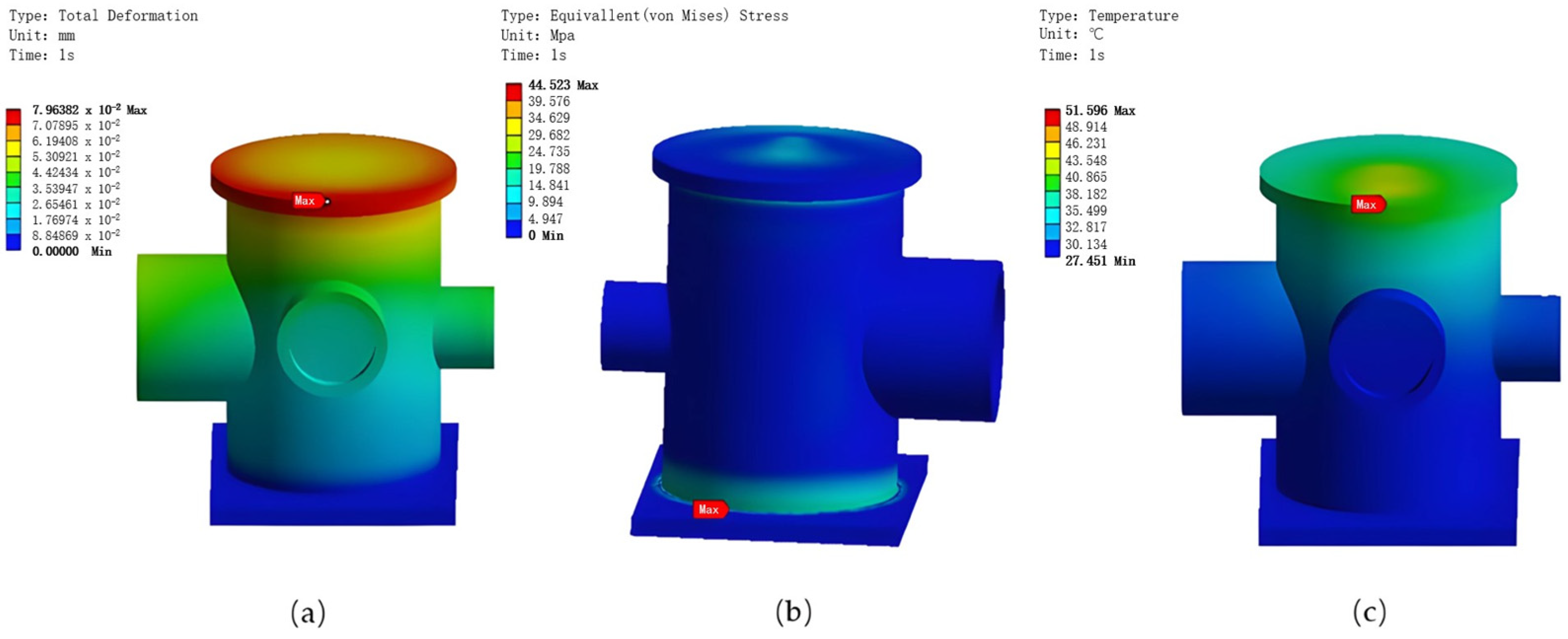
2.1.4. Vacuum System Module Design and Simulation

In accordance with the force requirements of the vacuum chamber, materials possessing ample strength, stiffness, toughness, heat resistance, corrosion resistance, and other pertinent physical and chemical properties are selected. In domestic film-forming equipment manufacturing, 304 stainless steel is the chosen material.
The shape of the vacuum vessel is determined based on the characteristics of the substrate and deposition source, with cylindrical and rectangular designs being the primary choices. Cylindrical designs offer high strength and are well suited for small- to medium-sized vessels, while rectangular designs optimize space utilization. For film-forming equipment, smaller- to medium-sized equipment typically adopts a vertical cylindrical design, while larger equipment leans towards a horizontal cylindrical configuration. The composite film preparation equipment embraces a vertical cylinder design, with the cylinder welded to the bottom plate. The schematic representation of the designed vacuum chamber structure is depicted in Figure 6. The cylindrical vacuum chamber features an inner diameter of 250 mm and a height of 360 mm, and the wall thickness is 7 mm. It is equipped with CF100 flanges and a quartz window, a CF60 flange interface to connect the molecular pump, an LF250 flange interface for installing the sputtering target and the sample stage, and a KF63 flange interface for integrating the evaporation module. Additionally, two adjustable needle valves at the rear control the air inlet, and a reserved 1/16-inch interface accommodates the mass spectrometer.
As the central space for experiments, a thorough analysis of the vacuum chamber’s strength, stiffness, and stability through performance simulation is essential. In real operational conditions, the vacuum chamber maintains an internal pressure of 0.0001 Pa and is exposed to an atmospheric pressure of 0.1 Mpa externally. Under equivalent conditions, a negative pressure of −0.1 MPa is applied internally to simulate evacuation. The vacuum chamber, placed on the electric control cabinet without considering its self-weight, undergoes structural static analysis. The results, illustrating the stress field distribution and deformation distribution, are presented in Figure 7. It can be seen from Figure 7a,b that under actual working conditions of the vacuum chamber, maximum deformation occurs at the center of the flange cover on the vacuum chamber, with the maximum value being 9.2926 × 10⁻³ mm. This value is very small and has almost no impact on the deformation and performance of the vacuum chamber. According to the simulation results in Figure 7b, the maximum deformation of the vacuum chamber is 9.29 × 10⁻³ mm. At this scale, the deformation of the vacuum chamber will not affect the overall equipment operation ecology, nor will it cause instability, so it meets the strain design requirements. Maximum stress occurs at the junction of the lower flange of the vacuum chamber cover and the inner wall of the vacuum chamber. The maximum value is 8.04 MPa, which is far less than the allowable stress of the material 150 MPa. Because this position is welded, maximum stress occurs at this position. It is also realistic, so the design is reasonable.
From Figure 8a,b, it is evident that under actual working conditions, maximum deformation occurs in the center of the upper flange cover, measuring 9.2926 × 10⁻³ mm. This value is sufficiently small, having no impact on the performance and aligning with the design requirements of staying within 0.1 mm. Maximum stress is observed in the lower flange and the inner wall junction, registering at 8.04 MPa, significantly below the permissible stress of 150 MPa. This outcome aligns with the actual welding conditions, affirming the reasonability of the design.
Under the specified conditions, an external air pressure of 105 Pa is applied to the vacuum chamber, and a thermodynamic coupling analysis simulation is executed to assess performance in vacuum and heated environments. In a vacuum setting, heat transfer occurs through contact position exchange and thermal radiation. Key parameters include a sputtering target heating source at 500 °C, substrate table heating at 100 °C, sputtering target and substrate table surface emissivity set at 0.8, and the vacuum cavity inner wall emissivity at 0.1. The temperature distribution results are then integrated into the static analysis module to complete the thermal coupling analysis. The obtained results for the stress field and deformation distribution are illustrated in Figure 8.
As depicted in Figure 8a,b, hot air radiation and sputtering target heat transfer affect the vacuum cover, resulting in a maximum deformation of 7.96 × 10⁻³ mm, well below the 0.1 mm threshold. The vacuum cavity remains unaffected, and maximum stress is observed in the vacuum cavity and the bottom plate weld, measuring 44.523 MPa. This value is significantly less than the permissible stress for 304 stainless steel, which is 150 MPa. Consequently, the structural design and material selection for the vacuum cavity align with the practical requirements.

2.2. Research on Film Thickness Prediction Algorithm

In the preceding chapters, our focus was on investigating the process and structural design of composite thin film preparation equipment, specifically addressing the magnetron sputtering and vacuum vapor deposition processes. This chapter focuses on achieving accurate predictions of the film thickness of composite films, delving into the design of a film thickness prediction model based on secondary integration learning. We utilized the PyCharm compiler software 2022.3.2 on the PC to execute the quadratic integration algorithm model, scripted in Python. Various algorithmic models were compared to validate the feasibility and advantages of the quadratic integration learning model.

2.2.1. Modeling of the Secondary Integration Learning Algorithm

The construction of a secondary integrated learning model involves the collection of input and output features, the creation of a dataset, its division into a training set and a test set, model training, and subsequent evaluation using performance metrics [30,31]. The specific process is depicted in Figure 9.

2.2.2. Feature Selection and Data Segmentation

In predicting the film thickness of the composite film, the characteristic inputs for the magnetron sputtering process include sputtering air pressure, current, and time, with the film thickness as the output. Similarly, for the vacuum evaporation process, the inputs encompass the evaporation amount and resistance evaporation current, yielding the film thickness as the output. The predicted film thicknesses from both approaches are aggregated to obtain the overall predicted film thickness of the composite film [32,33].
To enhance prediction accuracy, this article selects 15 samples for the magnetron sputtering process and 10 samples for the vacuum evaporation process. These samples were randomly divided into training and test sets, and the ratio of training and test sets was ensured to be 4:1.
Dataset division is a critical step. A standard method allocates four-fifths of the dataset for training and parameter optimization, reserving the remaining one-fifth for testing model performance. This approach ensures a relatively independent test set while retaining a substantial number of training sets, facilitating the accurate evaluation of model performance in real scenarios. The training and test datasets for both processes are presented in Table 1 and Table 2, with an asterisk denoting the training set.

2.2.3. Model Training and Effectiveness Evaluation

We constructed linear regression (LR), a random forest model (RFM), K-nearest neighbors (KNNs), decision tree (DT), and bagging and boosting models using Python in the PyCharm IDE. The performance of these models in terms of film thickness prediction was evaluated using metrics such as explained variance score (EV), mean absolute error (MAE), mean square error (MSE), mean absolute percentage error (MAPE), and the coefficient of determination R2 score [34,35,36,37].
We have selected 10 sets of experimental conditions for both magnetron sputtering and vacuum evaporation processes to compare the predicted(test) values from the models with the actual values. Figure 10 shows the comparison of the predicted results (Y_Pred) and the actual values (Y_true) obtained from 10 different experimental conditions in the magnetron sputtering process, using a linear regression model (a), decision tree model (b), random forest model (c), KNN model (d), bagging model (e), and boosting model (f). Similarly, Figure 11 shows the comparison in the vacuum evaporation process under 10 different experimental conditions using the same set of models [38,39]. This is applicable to Figure 10 and Figure 11. In the picture, X-axis: number of samples; Y_True: film thickness true value; Y_Pred: film thickness prediction.
Figure 11 illustrates the training effects of the four sub-models for the vacuum vapor deposition process—decision tree, random forest, KNN, and linear regression—consistently with the magnetron sputtering process. At the same time, the training effect of the quadratic integral model of the vacuum evaporation process is also depicted. In the training effect plot, the horizontal and vertical axes signify the same parameters as in the magnetron sputtering process. In the picture, X-axis: number of samples; Y_True: film thickness true value; Y_Pred: film thickness prediction.
Both Figure 10 and Figure 11 represent the comparison of the test results and actual results for each model in both the vacuum evaporation process and the magnetron sputtering process, revealing a close consistency between the predicted values and the actual values. Therefore, it is recommended to use the Bagging model and the Boosting model for secondary ensemble learning.

3. Results

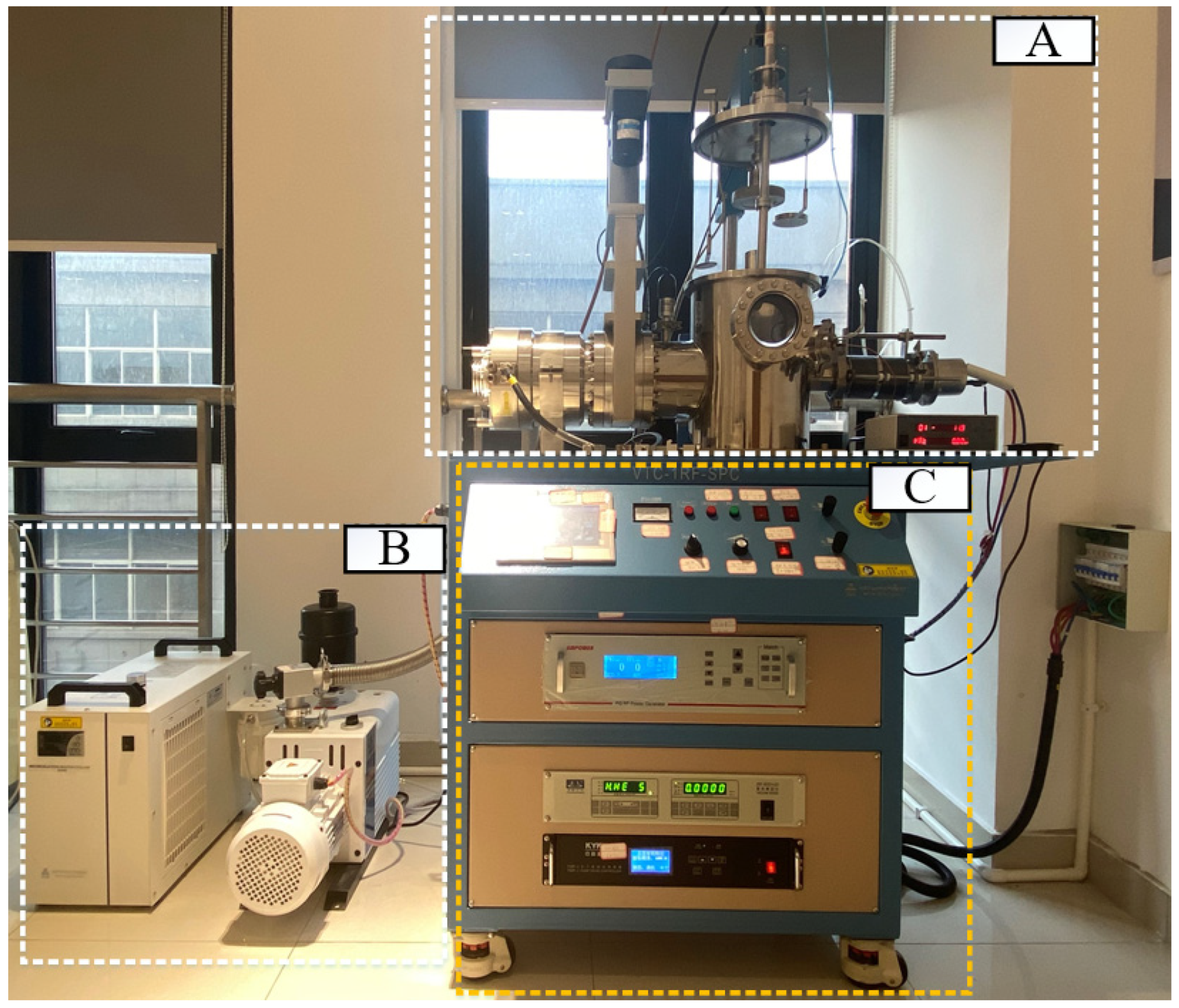
3.1. Platform Hardware Introduction

To validate the effectiveness of the selected equipment for composite film preparation, experimental validation was conducted. The choice of equipment was guided by considerations of applicability, precision, and adaptability to various process conditions. Drawing upon the preceding design and selection criteria, the experimental platform depicted in Figure 12 was constructed. This platform encompasses essential components such as the vacuum module, magnetron sputtering module, vacuum evaporation module, and transmission lifting module.

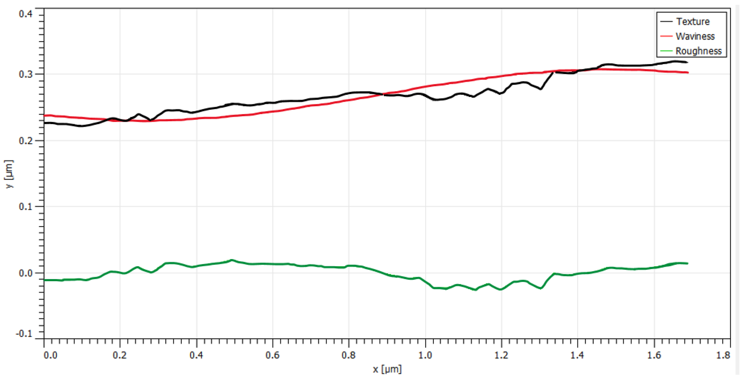
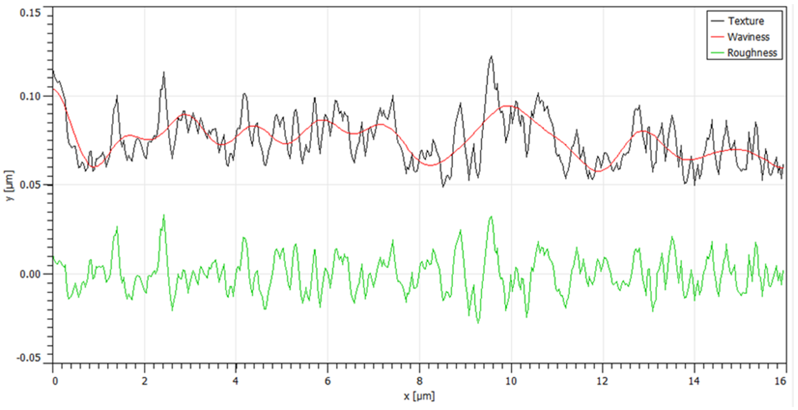
3.2. Surface Topography Inspection

The 2D–3D diagrams of Cr films, Cr-Al composite films, and Al-Cr composite films prepared by composite film preparation equipment are shown in Figure 13.
The 2D–3D morphology of the Cr substrate film, prepared through magnetron sputtering, is depicted in Figure 13a,b, with its maximum thickness measured at 0.22 μm.
Subsequently, an Al film was deposited on this Cr base film through vacuum vapor deposition, resulting in the formation of the Cr-Al composite film. The 2D–3D diagrams of this composite film are presented in Figure 13c,d, while the integrated diagrams illustrating the texture, waveform, and roughness of the Cr-Al composite film are shown in Figure 14. The analysis of Figure 13c,d and Figure 14 reveals that the thickness of the Cr-Al composite film reaches a maximum of 0.32 μm. Further examination of the texture, waveform, and roughness of the Cr-Al composite film indicates that the Al film, serving as the upper layer, exhibits the advantages of a uniformly distributed and relatively smooth surface.
The deposition method we used involves magnetron sputtering for the underlying Cr film and vacuum evaporation for the top Al film. This method has been proven to form uniform films over a large area. Our experimental results show that the thickness variation of the Cr-Al film we formed across the entire sample is less than 100 nm, demonstrating its good uniformity.
The same materials are used in different sequences to prepare Al-Cr composite films. The 2D and 3D diagrams and roughness and other parameter distribution diagrams are shown in Figure 13e,f and Figure 15.
As evidenced by Figure 13e,f and Figure 15, the peak of the Al-Cr composite film is 0.21 μm, with the entire film thickness fluctuating within the 0~0.21 μm range. The comprehensive diagram of the texture, waveform, and roughness of the Al-Cr composite film indicates a significant variation in roughness, which is attributed to vibrations or warping during the magnetron sputtering process. The texture and waveform in the diagram also exhibit considerable fluctuations. In conjunction with the two-dimensional and three-dimensional morphology of the Al-Cr composite film, it can be inferred that the presence of large-sized particles on the film surface, i.e., regional non-uniformity, causes this. The deepening of the grooves between large grains also leads to an increase in roughness. This analysis reveals that the magnetron sputtering process exhibits small-area non-uniformity and large-area uniformity, which may be caused by the inherent vibrations or warping in the magnetron sputtering process.

3.3. Algorithm Model Validation

Upon analyzing the results predicted by the established secondary integrated learning algorithmic model, the evaluation metrics for the magnetron sputtering process and vacuum evaporation process are presented in Table 3 and Table 4 below.
The evaluation indexes for the magnetron sputtering process prediction model (Table 3) reveal that the comparative ranking of the training model results for the magnetron sputtering process is as follows: bagging > DF > boosting > DT > KNN > LR. Meanwhile, for the vacuum evaporation process training model (Table 4), the comparative ranking of the results is as follows: bagging ≥ LR > boosting > DT > RF > KNN. Notably, the regression model fit value of the integrated learning bagging model achieves 100%, signifying a perfect model. When comparing the different regression models for both preparation processes, it is evident that in each approach, our designed secondary integrated learning bagging model demonstrates optimal performance, reaching 99% in the magnetron sputtering process and achieving a perfect 100% fit in the vacuum evaporation process. This suggests that the robust regression model designed with secondary integrated learning bagging surpasses ordinary weak machine algorithm models, substantiating its superior performance.

4. Discussion

This study undertook a comprehensive scheme design for the structure of composite film preparation equipment, successfully implementing the film thickness prediction function. Throughout the research process, the following key achievements were realized: (1) The mechanical structure of the composite thin film preparation equipment was systematically divided into different modules, completing the structural design of the core module. Simulation verification ensured the stability and reasonable strength stiffness of the process chamber. (2) The design and implementation of a regression model for predicting the film thickness of composite thin films were achieved. Input features included the sputtering air pressure, sputtering current, and sputtering time for magnetron sputtering process samples, as well as the evaporation amount and evaporation current for vacuum evaporation process samples. The film thickness served as the output feature for both process samples. (3) Experimental validation was conducted using the designed composite film preparation equipment. Cr-Al composite thin films were successfully prepared, and AFM surface morphology analysis confirmed the excellent performance and reliability of both the equipment and the Cr-Al composite films prepared.
Through the comparative analysis of the results of the Cr-Al composite film and the Al-Cr composite film, it is known that there is a step phenomenon on the surface of the single-layer Cr film sputtered by the magnetron in this device. When a composite film is prepared using vacuum evaporation, the step phenomenon will also exist, which is caused by the step-type bottom layer film. By comparing the three-dimensional morphology and height distribution of the two, it can be concluded that the Cr-Al film prepared by first magnetron sputtering and then vacuum evaporation by this device has better uniformity. The magnetron sputtered Cr film serves as the bottom layer, giving the Cr-Al composite film excellent step performance. Furthermore, the Al film prepared by vacuum evaporation as the upper functional layer has better surface uniformity and smoothness. This will allow for the performance of the composite film to be maximized, thereby enhancing its performance, providing this film with better application scenarios and fields.
In the future, the design of composite film preparation platforms should trend towards the greater integration of multiple processes to facilitate the preparation of more complex composite films. Additionally, a focus on enhanced prediction accuracy is recommended, exploring advanced techniques such as deep learning or neural networks to make the models more adaptable to dynamic and evolving preparation conditions.

Author Contributions

Conceptualization, C.L. and W.L.; methodology, C.L.; software, Y.G.; validation, G.C., W.L. and C.C.; formal analysis, J.W. investigation, N.Z.; resources, G.C.; data curation, C.L.; writing—original draft preparation, C.L.; writing—review and editing, C.L.; visualization, W.L.; supervision, W.L.; project administration, G.C.; funding acquisition, D.Z. and G.W. All authors have read and agreed to the published version of the manuscript.

Funding

This research was supported by Natural Science Foundation of Zhejiang Province, China (No. ZCLQ24E0101), Zhejiang Science and Technology Plan Project (No. 2022C01199), and Zhejiang Science and Technology Plan Project (No. 2023C01065).

Data Availability Statement

The original contributions presented in the study are included in the article, further inquiries can be directed to the corresponding author/s.

Conflicts of Interest

Author Niushan Zhang was employed by the company Changzhou Slav Intelligent Equipment Technology. Junyi Wu was employed by the company Sanmen Sanyou Technology. The remaining authors declare that the research was conducted in the absence of any commercial or financial relationships that could be construed as a potential conflict of interest.

References

  1. Abdelaziz, B.B.; Mustapha, N.; Bedja, I.M.; Aldaghri, O.; Idriss, H.; Ibrahem, M.; Ibnaouf, K.H. Spectral Behavior of a Conjugated Polymer MDMO-PPV Doped with ZnO Nanoparticles: Thin Films. Nanomaterials 2023, 13, 2405. [Google Scholar] [CrossRef]
  2. Behl, C.; Behlert, R.; Seiler, J.; Helke, C.; Shaporin, A.; Hiller, K. Characterization of Thin AlN/Ag/AlN-Reflector Stacks on Glass Substrates for MEMS Applications. Micro 2024, 4, 142–156. [Google Scholar] [CrossRef]
  3. Alanazi, T.I. Design and Device Numerical Analysis of Lead-Free Cs2AgBiBr6 Double Perovskite Solar Cell. Crystals 2023, 13, 267. [Google Scholar] [CrossRef]
  4. Ali, D.O.A.; Fabbiani, M.; Coulomb, L.; Bosc, S.; Villeroy, B.; Estournès, C.; Estournès, C.; Koza, M.M.; Beaudhuin, M.; Viennois, R. Reactive Spark Plasma Sintering and Thermoelectric Properties of Zintl Semiconducting Ca14Si19 Compound. Crystals 2023, 13, 262. [Google Scholar] [CrossRef]
  5. Gong, L.; Zhang, P.; Lou, Z.; Wei, Z.; Wu, Z.; Xu, J.; Chen, X.; Xu, W.; Wang, Y.; Gao, F. Effect of Bi3+ Doping on the Electronic Structure and Thermoelectric Properties of (Sr0.889−xLa0.111Bix)TiO2.963: First-Principles Calculations. Crystals 2023, 13, 178. [Google Scholar] [CrossRef]
  6. Brito, D.; Anacleto, P.; Pérez-Rodríguez, A.; Fonseca, J.; Santos, P.; Alves, M.; Cavalli, A.; Sharma, D.; Claro, M.S.; Nicoara, N.; et al. Antimony Selenide Solar Cells Fabricated by Hybrid Reactive Magnetron Sputtering. Nanomaterials 2023, 13, 2257. [Google Scholar] [CrossRef]
  7. Castillo, I.; Mishra, K.K.; Katiyar, R.S. Characterization of V2O3 Nanoscale Thin Films Prepared by DC Magnetron Sputtering Technique. Coatings 2022, 12, 649. [Google Scholar] [CrossRef]
  8. Ding, Y.; Wang, Y.; Chen, J.; Chen, W.; Hu, A.; Shu, Y.; Zhao, M. Substrate-Assisted Laser-Induced Breakdown Spectroscopy Combined with Variable Selection and Extreme Learning Machine for Quantitative Determination of Fenthion in Soybean Oil. Photonics 2024, 11, 129. [Google Scholar] [CrossRef]
  9. Stoddard, N.; Pimputkar, S. Progress in Ammonothermal Crystal Growth of Gallium Nitride from 2017–2023: Process, Defects and Devices. Crystals 2023, 13, 1004. [Google Scholar] [CrossRef]
  10. Zhou, F.; Zhao, Y.; Fu, F.; Liu, L.; Luo, Z. Thickness Nanoarchitectonics with Edge-Enhanced Raman, Polarization Raman, Optoelectronic Properties of GaS Nanosheets Devices. Crystals 2023, 13, 1506. [Google Scholar] [CrossRef]
  11. Estime, B.; Ren, D.; Sureshkumar, R. Tailored Fabrication of Plasmonic Film Light Filters for Enhanced Microalgal Growth and Biomass Composition. Nanomaterials 2023, 14, 44. [Google Scholar] [CrossRef] [PubMed]
  12. Hwang, S.; Han, Y.; Gardner, D.J. Characterization of CNC Nanoparticles Prepared via Ultrasonic-Assisted Spray Drying and Their Application in Composite Films. Nanomaterials 2023, 13, 2928. [Google Scholar] [CrossRef] [PubMed]
  13. Ji, S.; Zhu, J.; Yang, Y.; Zhang, H.; Zhang, Z.; Xia, Z.; Zhang, Z. Self-Attention-Augmented Generative Adversarial Networks for Data-Driven Modeling of Nanoscale Coating Manufacturing. Micromachines 2022, 13, 847. [Google Scholar] [CrossRef] [PubMed]
  14. Junrear, J.; Sakunasinha, P.; Chiangga, S. The Optimization of Metal Nitride Coupled Plasmon Waveguide Resonance Sensors Using a Genetic Algorithm for Sensing the Thickness and Refractive Index of Diamond-like Carbon Thin Films. Photonics 2022, 9, 332. [Google Scholar] [CrossRef]
  15. Kotlyar, V.; Nalimov, A.; Kovalev, A.; Stafeev, S. Optical Polarization Sensor Based on a Metalens. Sensors 2022, 22, 7870. [Google Scholar] [CrossRef] [PubMed]
  16. Ku, C.-A.; Yu, C.-Y.; Hung, C.-W.; Chung, C.-K. Advances in the Fabrication of Nanoporous Anodic Aluminum Oxide and Its Applications to Sensors: A Review. Nanomaterials 2023, 13, 2853. [Google Scholar] [CrossRef]
  17. Lee, M.; Kim, J.; Khine, M.T.; Kim, S.; Gandla, S. Facile Transfer of Spray-Coated Ultrathin AgNWs Composite onto the Skin for Electrophysiological Sensors. Nanomaterials 2023, 13, 2467. [Google Scholar] [CrossRef] [PubMed]
  18. Lin, Q.; Wang, Z.; Meng, Q.; Mao, Q.; Xian, D.; Tian, B. A Co-Sputtering Process Optimization for the Preparation of FeGaB Alloy Magnetostrictive Thin Films. Nanomaterials 2023, 13, 2948. [Google Scholar] [CrossRef]
  19. Ling, L.; Zhang, X.; Hu, X.; Fu, Y.; Yang, D.; Liang, E.; Chen, Y. Research on Spraying Quality Prediction Algorithm for Automated Robot Spraying Based on KHPO-ELM Neural Network. Machines 2024, 12, 100. [Google Scholar] [CrossRef]
  20. Loghin, F.; Rivadeneyra, A.; Becherer, M.; Lugli, P.; Bobinger, M. A Facile and Efficient Protocol for Preparing Residual-Free Single-Walled Carbon Nanotube Films for Stable Sensing Applications. Nanomaterials 2019, 9, 471. [Google Scholar] [CrossRef]
  21. Hashimoto, T.; Letts, E.R.; Key, D. Progress in Near-Equilibrium Ammonothermal (NEAT) Growth of GaN Substrates for GaN-on-GaN Semiconductor Devices. Crystals 2022, 12, 1085. [Google Scholar] [CrossRef]
  22. Heng, C.; Wang, X.; Zhao, C.; Wu, G.; Lv, Y.; Wu, H.; Zhao, M.; Finstad, T.G. Ultrathin Rare-Earth-Doped MoS2 Crystalline Films Prepared with Magnetron Sputtering and Ar + H2 Post-Annealing. Crystals 2023, 13, 308. [Google Scholar] [CrossRef]
  23. Luo, J.; Khattinejad, R.; Assari, A.; Tayyebi, M.; Hamawandi, B. Microstructure, Mechanical and Thermal Properties of Al/Cu/SiC Laminated Composites, Fabricated by the ARB and CARB Processes. Crystals 2023, 13, 354. [Google Scholar] [CrossRef]
  24. Manjunath, M.; Hausner, S.; Heine, A.; De Baets, P.; Fauconnier, D. Electrical Impedance Spectroscopy for Precise Film Thickness Assessment in Line Contacts. Lubricants 2024, 12, 51. [Google Scholar] [CrossRef]
  25. Martínez, C.; Arcos, C.; Briones, F.; Machado, I.; Sancy, M.; Bustamante, M. The Effect of Adding CeO2 Nanoparticles to Cu–Ni–Al Alloy for High Temperatures Applications. Nanomaterials 2024, 14, 143. [Google Scholar] [CrossRef] [PubMed]
  26. Michman, E.; Oded, M.; Shenhar, R. Dual Block Copolymer Morphologies in Ultrathin Films on Topographic Substrates: The Effect of Film Curvature. Polymers 2022, 14, 2377. [Google Scholar] [CrossRef] [PubMed]
  27. Park, H.H.; Fermin, D.J. Recent Developments in Atomic Layer Deposition of Functional Overlayers in Perovskite Solar Cells. Nanomaterials 2023, 13, 3112. [Google Scholar] [CrossRef] [PubMed]
  28. Redka, D.; Buttberg, M.; Franz, G. Chemical Vapor Deposition of Longitudinal Homogeneous Parylene Thin-Films inside Narrow Tubes. Processes 2022, 10, 1982. [Google Scholar] [CrossRef]
  29. Wang, J.; Pan, Y.; Zhao, M.; Ma, P.; Lv, S.; Huang, Y. Computational Fluid Dynamics Numerical Simulation on Flow Behavior of Molten Slag–Metal Mixture over a Spinning Cup. Processes 2024, 12, 372. [Google Scholar] [CrossRef]
  30. Zhang, Q.; Li, H.; Li, Y.; Wang, H.; Lu, K. A Dynamic Permeability Model in Shale Matrix after Hydraulic Fracturing: Considering Mineral and Pore Size Distribution, Dynamic Gas Entrapment and Variation in Poromechanics. Processes 2024, 12, 117. [Google Scholar] [CrossRef]
  31. Zhou, W.-Y.; Chen, H.-F.; Tseng, X.-L.; Lo, H.-H.; Wang, P.J.; Jiang, M.-Y.; Fuh, Y.-K.; Li, T.T. Impact of Pulse Parameters of a DC Power Generator on the Microstructural and Mechanical Properties of Sputtered AlN Film with In-Situ OES Data Analysis. Materials 2023, 16, 3015. [Google Scholar] [CrossRef] [PubMed]
  32. Calabretta, M.; Sitta, A.; Oliveri, S.M.; Sequenzia, G. Warpage Behavior on Silicon Semiconductor Device: The Impact of Thick Copper Metallization. Appl. Sci. 2021, 11, 5140. [Google Scholar] [CrossRef]
  33. Grzywacz, H.; Jenczyk, P.; Milczarek, M.; Michałowski, M.; Jarząbek, D.M. Burger Model as the Best Option for Modeling of Viscoelastic Behavior of Resists for Nanoimprint Lithography. Materials 2021, 14, 6639. [Google Scholar] [CrossRef]
  34. Wang, Y.-F.; Yoshida, J.; Takeda, Y.; Yoshida, A.; Kaneko, T.; Sekine, T.; Kumaki, D.; Tokito, S. Printed Composite Film with Microporous/Micropyramid Hybrid Conductive Architecture for Multifunctional Flexible Force Sensors. Nanomaterials 2023, 14, 63. [Google Scholar] [CrossRef]
  35. Wu, R.; Hu, Y.; Li, P.; Peng, J.; Hu, J.; Yang, M.; Chen, D.; Guo, Y.; Zhang, Q.; Xie, X.; et al. Controlled Epitaxial Growth and Atomically Sharp Interface of Graphene/Ferromagnetic Heterostructure via Ambient Pressure Chemical Vapor Deposition. Nanomaterials 2021, 11, 3112. [Google Scholar] [CrossRef] [PubMed]
  36. Yazdani, S.; Phillips, J.; Mosey, A.; Bsaibes, T.; Decca, R.; Cheng, R. Study of the Long-Range Exchange Coupling in Nd-Fe-B/Ti/Fe Multilayered Structure. Crystals 2024, 14, 119. [Google Scholar] [CrossRef]
  37. Ying, M.; Liu, X.; Zhang, Y.; Zhang, C. Optimizing Load Capacity Predictions in Gas Foil Thrust Bearings: A Novel Full-Ramp Model. Lubricants 2024, 12, 76. [Google Scholar] [CrossRef]
  38. Zhu, C.; Jin, L.; Li, W.; Han, S.; Yan, J. The Prediction of Wear Depth Based on Machine Learning Algorithms. Lubricants 2024, 12, 34. [Google Scholar] [CrossRef]
  39. Zou, T.; Kang, L.; Zhang, D.; Li, J.; Zheng, Z.; Peng, X. Polyethylene Terephthalate Composite Films with Enhanced Flame Retardancy and Gas Barrier Properties via Self-Assembly Nanocoating. Nanomaterials 2023, 13, 2018. [Google Scholar] [CrossRef]
Figure 1. Assembly diagram of composite film preparation equipment. 1—sputtering system; 2—process chamber; 3—evaporation system; 4—water cooler; 5—vacuum pump; 6—electronic control cabinet; 7—molecular pump; 8—baffle valve; 9—transmission system.
Crystals 14 00389 g001
Figure 2. Schematic diagram of sputtering system. (a) Two-dimensional schematic; 1—capacitance manometer; 2—grounding shield; 3—substrate; 4—sample stage baffle; 5—height-adjustable substrate stage; 6—sputtering target head baffle; 7—ion piezometer; 8—grounding shield; 9—target head holder; 10—sputtering gas control valve; 11—connecting vacuum pump; 12—target material; 13—substrate heater; (b) physical image of the sputtering system.
Crystals 14 00389 g002
Figure 3. Evaporation system structure principle sketch: 1—capacitance manometer; 2—substrate heater; 3—substrate; 4—height-adjustable substrate table; 5—temperature gauge; 6—bellows heat transfer assembly; 7—heat source flange for heating platform; 8—ground shield; 9—water-cooled piping; 10—heating platform for evaporation system; 11—evaporation target; 12—evaporation crucible; 13—connection vacuum pump.
Crystals 14 00389 g003
Figure 4. Structural design diagram.
Crystals 14 00389 g004
Figure 5. Physical image.
Crystals 14 00389 g005
Figure 6. Vacuum chamber structure.
Crystals 14 00389 g006
Figure 7. Static stress field distribution and deformation distribution resultant plots; (a) static stress field distribution; (b) static deformation field distribution.
Crystals 14 00389 g007
Figure 8. Thermal coupling analysis of the stress deformation results of the figure; (a) thermal coupling deformation field distribution; (b) thermal coupling strain field distribution; (c) temperature distribution map.
Crystals 14 00389 g008
Figure 9. Secondary integration learning modeling process.
Crystals 14 00389 g009
Figure 10. Comparison chart of the test results from six prediction models versus the actual results in the magnetron sputtering process. (a) Comparison chart of the Linear Regression model; (b) Comparison chart of the Decision Tree model; (c) Comparison chart of the Random Forest mode; (d) Comparison chart of the KNN model; (e) Comparison chart of the Bagging model; (f) Comparison chart of the Boosting model.
Crystals 14 00389 g010
Figure 11. Comparison chart of the test results from six prediction models versus the actual results in the vacuum evaporation process. (a) Comparison chart of the Linear Regression model; (b) Comparison chart of the Decision Tree model; (c) Comparison chart of the Random Forest mode; (d) Comparison chart of the KNN model; (e) Comparison chart of the Bagging model; (f) Comparison chart of the Boosting model.
Crystals 14 00389 g011
Figure 12. Experimental platform of composite film preparation equipment. (A) Mechanical structure of hybrid film preparation equipment; (B) execution equipment of hybrid film preparation equipment; (C) composite film preparation equipment.
Crystals 14 00389 g012
Figure 13. (a) Two-dimensional morphology of Cr bottom membrane; (b) three-dimensional morphology of Cr base film; (c) two-dimensional morphology of Cr-Al composite film; (d) three-dimensional morphology of Cr-Al composite film; (e) two-dimensional morphology of Al-Cr composite film; (f) three-dimensional morphology of Al-Cr composite film.
Crystals 14 00389 g013
Figure 14. Combined texture, waveform, and roughness of Cr-Al composite film; x-axis: film expansion length; y-axis: texture, waviness, and roughness change value.
Crystals 14 00389 g014
Figure 15. Combined texture, waveform, and roughness of Al-Cr composite film; x-axis: film expansion length; y-axis: texture, waviness, and roughness change value.
Crystals 14 00389 g015
Table 1. Magnetron sputtering process dataset division: the data group with * is the training set used to train the model, and the data group without * is the test set used to evaluate the model.
Dataset No.Sputtering Air Pressure/PaSputtering Current/mASputtering Time/sFilm Thickness/nm
1 *0.71201010.6
20.81201410.4
3 *1.41203016.0
4 *1.51201410.8
50.91201211.2
6 *0.81202011.5
7 *0.71301012.3
8 *0.81301411.9
9 *1.41303017.5
10 *1.51301413.3
110.81102010.5
12 *0.91201311.1
13 *0.81201810.8
14 *0.81203019.3
15 *0.91203525.4
Table 2. Vacuum vapor deposition process dataset division: the data group with * is the training set used to train the model, and the data group without * is the test set used to evaluate the model.
Dataset No.Evaporation Amount/gResistance to Vaporization Current/AFilm Thickness/nm
1 *0.2300.2
2 *0.4300.3
30.6300.4
4 *0.8300.6
5 *1.0250.7
6 *1.0300.7
7 *1.0350.7
8 *1.0400.8
91.2300.8
10 *1.5301.1
Table 3. Metrics for evaluating the regression model of a magnetron sputtering process.
Assessment of IndicatorsLRKNNDTRFBaggingBoosting
EV0.910.950.970.990.990.98
MAE146.4672.9465.3932.0131.8751.15
MSE33,237.0120,529.719951.063173.003035.978242.24
MAPE59.4412.2212.866.427.019.98
R20.910.940.970.990.990.98
Table 4. Regression model evaluation metrics for the vacuum evaporation process.
Assessment of IndicatorsLRKNNDTRFBaggingBoosting
EV1.000.870.980.981.001.00
MAE0.010.080.040.040.010.01
MSE0.000.010.000.000.000.00
MAPE1.1517.775.848.281.151.11
R21.000.870.980.971.001.00
Disclaimer/Publisher’s Note: The statements, opinions and data contained in all publications are solely those of the individual author(s) and contributor(s) and not of MDPI and/or the editor(s). MDPI and/or the editor(s) disclaim responsibility for any injury to people or property resulting from any ideas, methods, instructions or products referred to in the content.

