

Decoding Material Structures with Scanning Electron Diffraction Techniques
Department of Physics, Gachon University, Seongnam 13120, Republic of Korea
Crystals 2024, 14(3), 275; https://doi.org/10.3390/cryst14030275
Submission received: 10 February 2024
/
Revised: 2 March 2024
/
Accepted: 6 March 2024
/
Published: 14 March 2024
(This article belongs to the Special Issue Application of X-ray and Electron to Crystal Structure Characterization)
Abstract
:Recent advancements in electron detectors and computing power have revolutionized the rapid recording of millions of 2D diffraction patterns across a grid of probe positions, known as four-dimensional scanning transmission electron microscopy (4D-STEM). These datasets serve as the foundation for innovative STEM imaging techniques like integrated center of mass (iCOM) and symmetry STEM (S-STEM). This paper delves into the application of 4D-STEM datasets for diffraction analysis. We therefore use the term scanning electron diffraction (SED) instead of 4D-STEM in this review. We comprehensively explore groundbreaking diffraction methods based on SED, structured into two main segments: (i) utilizing an atomic-scale electron probe and (ii) employing a nanoscale electron probe. Achieving an atomic-scale electron probe necessitates a significant convergence angle (α > 30 mrad), leading to interference between direct and diffracted beams, distinguishing it from its nanoscale counterpart. Additionally, integrating machine learning approaches with SED experiments holds promise in various directions, as discussed in this review. Our aim is to equip materials scientists with valuable insights for characterizing atomic structures using cutting-edge SED techniques.
1. Introduction
Cowley initially explored scanning electron nanodiffraction (SEND) [1], a method that captures electron diffraction data for each position scanned by the electron probe. However, this technique did not gain widespread adoption mainly due to the recording of diffraction patterns using taped videos, resulting in low-quality data. Analyzing information from these taped videos also posed significant challenges. In recent years, there has been a renewed interest in the same method, now referred to as four-dimensional scanning transmission electron microscopy (4D-STEM) [2,3], driven by advancements in electron detectors [4,5,6,7,8] and enhanced computational capabilities. The nomenclature 4D-STEM stems from its collection of a four-dimensional (4D) diffraction dataset, namely, the electron diffraction pattern in momentum space (kx, ky) for each probe position in real space (x, y) (see Figure 1).
Currently, 4D-STEM is paving the way for innovative STEM imaging techniques and position-dependent diffraction methods. Within this single dataset, diverse STEM images such as bright field (BF), annular bright field (ABF), medium-angle annular dark field (MAADF), and high-angle annular dark field (HAADF) can be reconstructed [9]. Novel atomic-scale imaging techniques, including integrated center of mass (iCOM) [10,11] and symmetry STEM (S-STEM) [12], are introduced based on this dataset, revealing concealed atomic-scale information such as electric field, electron charge density, and local symmetry. Emphasizing raw data for STEM image construction, the term “4D-STEM dataset” reflects its primary role. Apart from serving as the basis for image construction, the diffraction patterns within 4D-STEM datasets also contain local crystallographic information. Thus, interpreting these patterns is equally crucial. In this review, we focus on interpreting diffraction patterns within the 4D-STEM dataset. We therefore use the term scanning electron diffraction (SED) instead of 4D-STEM in this review. The interpretation of diffraction patterns differs significantly based on the electron probe utilized, whether atomic scale or nanoscale. Raw data from atomic-scale electron probes present challenges for direct interpretation [13,14], requiring post-processing like position averaging or the integration of deep learning methods to extract structural information. Meanwhile, raw data from nanoscale electron probes contain interpretable structural information. Each diffraction pattern in the SED dataset corresponds to patterns obtained via conventional electron diffraction techniques, nanobeam electron diffraction (NED) and convergent beam electron diffraction (CBED), to be further discussed in Section 3.
The initial groundbreaking shift in recording electron diffraction patterns involves using a charge-coupled device (CCD) with digital readout in conjunction with a scintillator. Some pioneering groups began developing SED techniques with CCD, utilizing dedicated hardware to synchronize scanning and diffraction patterns [15] or implementing computer control for both TEM and CCD cameras [16]. However, CCD has limitations that hinder the widespread adoption of SED techniques, such as limited readout speed and dynamic range. The true leap in SED technologies is credited to the emergence of novel electron detectors: the monolithic active pixel sensor (APS) [6] and the hybrid pixel array detector (PAD) [5]. APS, composed of CMOS chips with a sensitive doped epitaxial layer, generates low-energy electrons as high-energy electrons pass through. These diffuse toward sensor diodes for correction and readout using CMOS electronics. This detector requires a low electron dose due to high-density electrons hindering individual electron strike localization, enabling single electron counting and fast readout speed but with a relatively low dynamic range [6]. PAD, an array of photodiodes bump-bonded to application-specific integrated circuits, employs high-gain integration and counting circuitry in each pixel, providing single electron counting, high dynamic range, and fast readout speeds [5]. Although suitable for most 4D-STEM experiments, PAD faces challenges in pixel integration, resulting in a low number of pixels. Notable commercially available APSs include Gatan K2 (or K3) and Direct Electrons DE-16 (or DE-64) [8], while available PADs encompass Thermo Scientific EMPAD [7] and Dectris QUADRO.
Enhanced computational capabilities, marked by increased processing speeds and the evolution of open libraries, are bolstering the popularity of SED technologies alongside advancements in electron detectors. Individual SED datasets, each several hundred gigabytes in size, pose impractical processing challenges without robust computational resources. Noteworthy Python libraries like HyperSpy, pyXem, LiberTEM, Pycrography, and py4DSTEM play a crucial role in dataset management [2]. The SED datasets, with intricate diffraction patterns and substantial size, conceal structural information. Accordingly, progress in machine learning accelerates the application of SED datasets for atomic- and nanoscale structural analysis [17]. Linear dimensionality reduction (DR) techniques like principal component analysis (PCA), independent component analysis (ICA), and non-negative matrix factorization (NMF) have been applied to analyze SED data. These techniques decompose a data matrix into a linear combination of loading vectors, each with different constraints in the decomposition process. However, limitations arise when dealing with nonlinear and complex data, where the raw data cannot be accurately described by a linear combination of components. In such cases, more sophisticated deep learning techniques, including supervised methods like artificial neural networks (ANNs), convolutional neural networks (CNNs) and generative adversarial networks (GANs), as well as unsupervised approaches employing autoencoders, have been embraced to unveil these intricate characteristics. This review will also explore various applications of dimensionality reduction and deep learning techniques in decoding SED datasets.
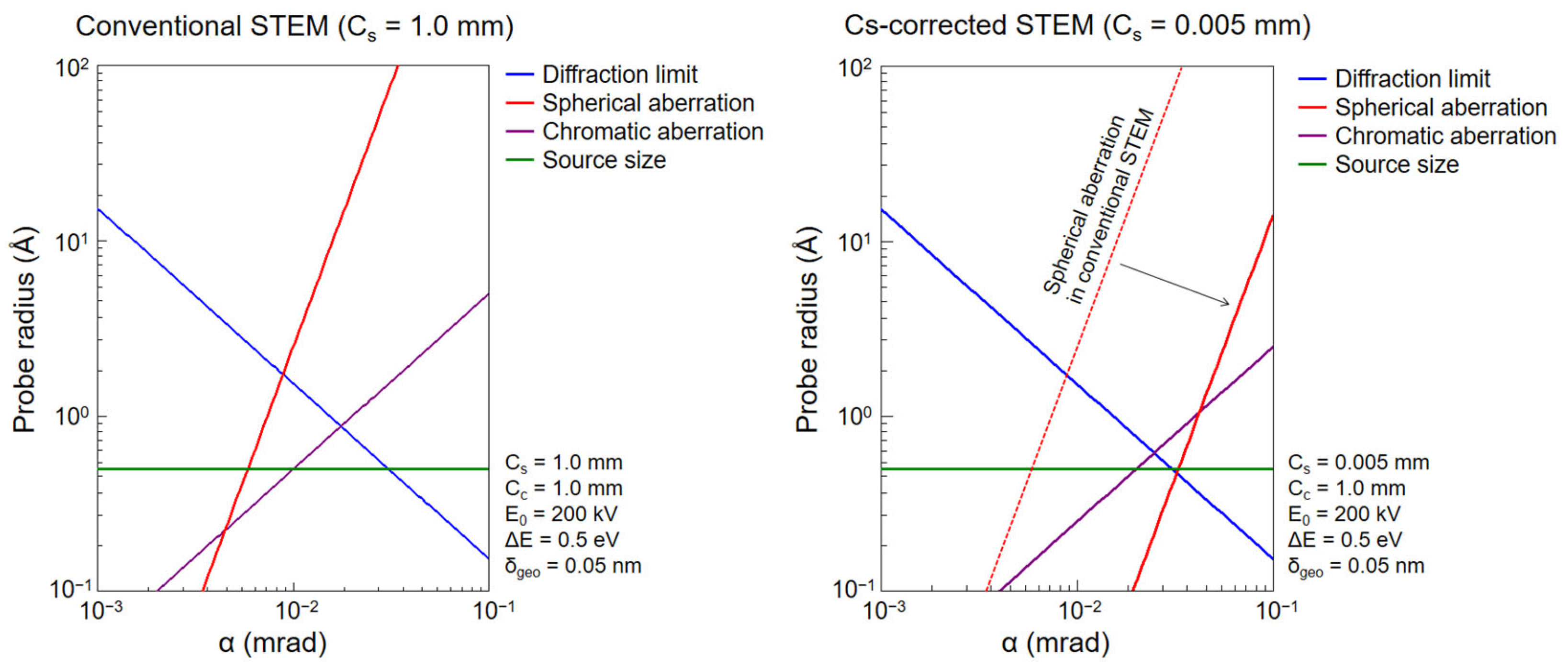
The size of the electron probe is influenced by four key factors: the diffraction limit, spherical aberration, chromatic aberration, and effective source size [18]. In Figure 2a, these factors are illustrated in relation to the convergence angle of the electron probe, highlighting the existence of an optimal convergence angle for each electron microscope to achieve the smallest electron probe. Crucially, the radius of the electron probe is inversely proportional to the convergence angle at low angles due to the diffraction limit. A convergence angle of a few milliradians result in a nanoscale electron probe, whereas that of thirty-to-forty milliradians is required for achieving an atomic-scale electron probe. The convergence angle also determines the radius of diffraction spots in momentum space, as illustrated in Figure 2b. In the case of a finite convergence angle, diffraction spots transform into diffraction disks, encapsulating a wealth of structural information. This electron diffraction technique with a finite convergence angle is termed CBED. For atomic-scale electron probes, overlapping CBED disks are unavoidable due to the necessity of a large convergence angle for achieving small electron probes. The interference patterns in the overlapped region, influenced by lens aberrations and electron multiple scattering, are complex, making the extraction of local crystallographic information from raw atomic-scale CBED patterns nearly impractical [14]. However, the interpretation of these patterns garners significant attention due to their highest spatial resolution among diffraction techniques, and a few methods have been proposed to extract novel information from these datasets, which will be discussed in the following chapter.
This review concentrates on extracting local crystallographic information from diffraction patterns in the SED dataset, categorizing analytical methods into two groups: (i) SED utilizing an atomic-scale electron probe and (ii) SED employing a nanoscale electron probe. It is worth noting again that we use the term SED instead of 4D-STEM throughout this article to emphasize the focus on analyzing diffraction patterns within this extensive dataset. The review excludes 4D-STEM-based imaging techniques such as iCOM, S-STEM, ptychography, etc., and interested readers are referred to excellent review articles on these topics. The aim is to introduce diffraction characterization methods to materials scientists unfamiliar with the rich possibilities offered by SED datasets.
2. SED Using an Atomic-Scale Electron Probe
The introduction of spherical aberration correctors has shifted the graph illustrating the impact of spherical aberration to the right (refer to Figure A1 in Appendix A). This shift leads to an increased optimal convergence angle and a probe size extending into sub-angstrom dimensions, fundamentally revolutionizing STEM techniques for achieving atomic-scale imaging and spectroscopies [19,20]. The use of atomic-scale STEM imaging combined with spectroscopies resolves numerous material issues [21,22,23]. However, the atomic-scale electron probe has not been applied to CBED analysis due to the inevitability of interference in the overlapped CBED region. Overlapped CBED disks are notably affected by lens aberrations and electron multiple scattering [14], making it a formidable task to extract structural information from diffraction patterns.
LeBeau, J. M. et al. introduced the concept of position-averaged CBED (PACBED) [24]. PACBED involves recording CBED pattern while rapidly scanning the atomic-scale probe across the image area. Position averaging eliminates interference between overlapping CBED disks, yet it remarkably preserves critical structural information, including thickness, tilt, local symmetry (octahedral tilt and polarity), and crystal stoichiometry. For example, Hwang, J. et al. demonstrated the determination of octahedral tilt patterns and angles in ultrathin LaNiO3 thin films using PACBED [25] (Figure 3a). Furthermore, C. Ophus et al. showcased SED-based PACBED [26] (Figure 3b). They acquired an SED dataset using an atomic-scale electron probe and averaged raw CBED patterns through post-processing. From the post-processed PACBED, they determined the local composition in a LaMnO3–SrTiO3 superlattice. Their work further demonstrates that interference between overlapping disks is effectively eliminated by averaging the diffraction patterns within the unit cell area.
PACBED analysis traditionally involves comparing experimental patterns with a library of simulated patterns to find the best match, a process that typically relies on human judgment or least square fitting, making it subjective and time consuming. However, deep learning has revolutionized PACBED analysis, enabling automatic assessments without human intervention. Xu, W. and LeBeau, J. M. demonstrated the capability of CNN to automatically analyze PACBED, incorporating parameters such as zero-order disk size, center position, rotation, and sample details like thickness and tilt [27]. Recently, Kim, Y. H. et al. utilized a hybrid deep CNN, combining supervised and unsupervised components, to analyze SED-based PACBED patterns in polycrystalline Hf0.5Zn0.5O2 films [28] (Figure 3c). Their study highlighted that deep learning can effectively extract crystallographic information from PACBED patterns, even though the patterns are averaged over a small area of only 2 nm2.
Figure 3.
SED using an atomic-scale electron probe. Position averaging eliminates interference from overlapping CBED disks. (a) Original position-averaged CBED (PACBED), from Hwang, J. et al. (2012). (Reprinted with permission from Ref. [25]. Copyright 2012 American Institute of Physics). (b) SED-based PACBED, from Ophus, C. et al. (2017). (Reprinted with permission from Ref. [26]. Copyright 2017 American Institute of Physics). (c) Integration of deep learning in SED-based PACBED, from Kim, Y.-H. et al. (2022). (Reprinted with permission from Ref. [28]. Copyright 2022 Wiley-VCH Verlag GmbH & Co. KGaA, Weinheim, Germany). (d) Atomic-column-sensitive PACBED using SED, from Zheng, C. et al. (2020). (Reprinted with permission from Ref. [29]. Copyright 2020 Elsevier).

Zheng, C. et al. showed that averaging CBED patterns near each atomic column still retains structural information [29] (Figure 3d). They illustrated the determination of Sr column thickness in SrTiO3 using atomic-column-sensitive PACBED, integrating the deep learning CNN method. It is important to note that the electron beam propagates not only along a single atomic column where it is positioned but also along multiple nearby columns. Nonetheless, the primary diffraction contribution typically arises from the atomic column where the electron beam is located, thereby offering valuable structural insights. Atomic-column-sensitive PACBED based on SED holds promise for discerning specific structural details at the atomic column level, such as octahedral tilt and local misorientation. Additionally, this technique may offer a means to detect the type and location of point defects like vacancies. Point defects and associated local distortions can disrupt the electron propagation path, resulting in distinctive scattering distributions in atomic-column-sensitive PACBED patterns. Notably, demonstrating point defect detection in SED-based PACBED must overcome practical challenges, such as the diffusion of point defects during the electron probe scan.
3. SED Using a Nanoscale Electron Probe
A large convergence angle, leading to a CBED disk overlap, is not necessary for a nanoscale electron probe. To note, a large convergence angle (>30 mrad) is essential to form an atomic-scale electron probe. If CBED disks are not overlapped, the interpretation of diffraction patterns becomes more straightforward. Conventionally, nanoscale electron probe diffractions fall into two categories: NED and CBED. The primary distinction lies in the convergence angle, with CBED having a larger angle than NED. The SED technique with a nanoscale electron probe involves acquiring NED and CBED patterns with probe-position dependence, indicating that the same methodology used to interpret NED and CBED patterns can be applied to analyze the SED dataset [14]. In this chapter, we will not differentiate between NED and CBED without disk overlap and will refer to both techniques as NED. SED with a nanoscale electron probe has seen continuous advancements over several decades; previously, CCD cameras are employed for initial SED experiments. Popularity surged with ultrafast electron detectors like APS and PAD. These detectors can capture ten thousand diffraction patterns per second, nearly matching STEM imaging timescales. This advancement not only enhances the spatial resolution and field of view of SED datasets but also offers a way to minimize electron beam damage by reducing the dwell time of the electron probe (total dose).
As an additional note, the precession of the electron beam, involving continuous rotation around a cone of projection angles, has been often employed in NED experiments [30]. Precession offers two key advantages. Firstly, it increases the number of reflections in diffraction patterns, enhancing the number of diffraction spots even when the specimen is not perfectly aligned. This proves beneficial for analyzing polycrystalline materials. Secondly, it reduces dynamical scattering effects, facilitating the application of kinematic theory for interpreting diffraction spot intensities. Consequently, the structural refinement traditionally conducted through X-ray diffraction becomes achievable in electron microscopy with the adoption of a precession electron beam [31]. The precession of the electron beam is also often beneficial in SED across various directions.
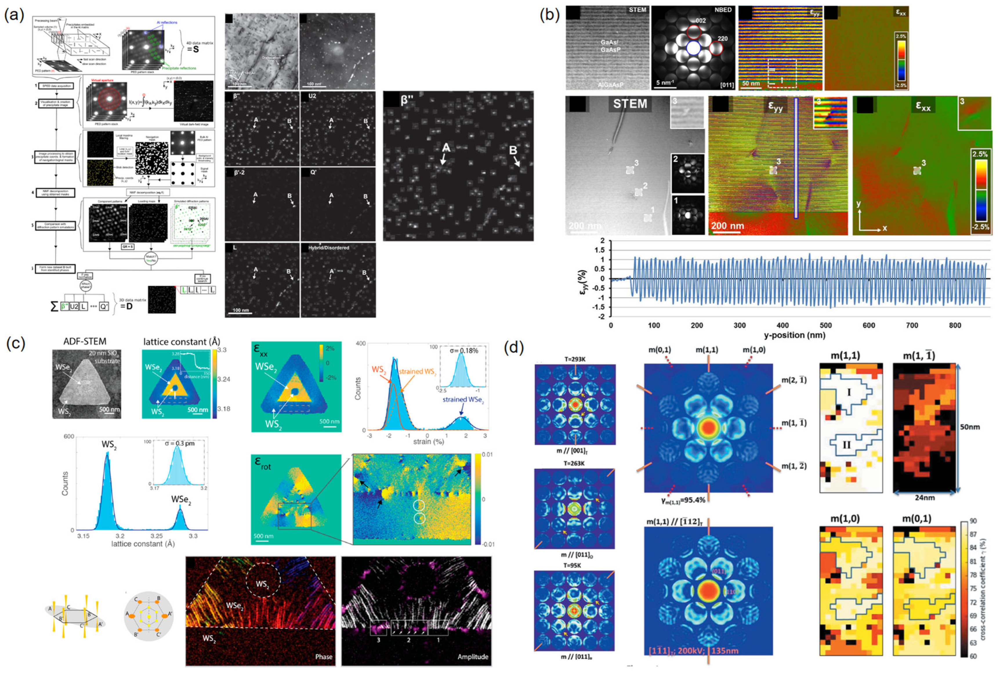
SED using a nanoscale electron probe finds direct application in phase and orientation mapping at the nanometer scale. The initial approach involves mapping a specific phase or orientation using a virtual aperture on the SED dataset, akin to the dark-field mode in TEM imaging. The second approach entails mapping phases and orientation by comparing diffraction patterns with a library of simulated ones. The commercially available ASTAR system adopts this approach, incorporating electron beam precession [15]. Here, electron beam precession is adopted to enhance reflections in the diffraction space and reduces dynamical scattering effects to enable a comparison between diffraction patterns and kinematically simulated ones. In addition, ASTAR streamlines the comparison between experimental and simulated diffraction patterns through template matching processes. The third approach integrates machine learning to achieve phase and orientational mapping, encompassing both linear dimensionality reduction (DR) techniques and deep learning methods to analyze SED datasets. Sunde, J. K. et al. demonstrated spatial phase distribution mapping in alloy microstructures using SED datasets with NMF [32] (Figure 4a). Linear DR techniques such as PCA, ICA, and NMF play a critical role when diffraction patterns can be decomposed into a linear combination of representative loading vectors. On another front, Yuan, R. et al. utilized an ANN for crystal orientation mapping in a GaSb thin sample with bending near a crack [33]. The non-linear variations in diffraction patterns make deep learning methods more effective than linear DR techniques for analysis.
Variations in lattice parameters within crystalline materials significantly influence the physical properties of functional materials, making accurate strain measurement a key focus in TEM. Methods such as NED (or CBED), atomic-scale imaging and quantification like geometrical phase analysis (GPA) [34] and peak pairs analysis (PPA) [35], and electron holography [36] have been used to assess strains in TEM. Two approaches are employed to estimate strain using NED: one directly measures the distance between diffraction spots for local lattice parameter estimations [37], and the other utilizes higher-order Laue zone (HOLZ) lines within NED disks [38,39] for the same purpose. In principle, both approaches can be applied to SED experiments. However, while the former has been integrated into SED experiments, the latter is limited in its use in SED experiments. Analyzing HOLZ lines within NED disks offers high precision, but automating the analysis proves challenging due to intricate numerical simulations and complex quantification. For strain measurement using atomic-imaging-based quantification and electron holography, consulting other review papers or books is recommended.
SED-based strain measurements offer the benefit of measuring strains with high spatial resolution and a large field of view. Ozdol, V. B. et al. demonstrates precise strain mapping with 0.1% accuracy and 1 nm lateral resolution over an 1 μm field of view in GaAs/GaAsP heterostructures, using SED techniques with a Gatan K2 direct camera [40] (Figure 4b). Han, Y. M. et al. achieved 0.3 pm precision in mapping lattice distortions across a few micrometer field-of-view in WSe2/WS2 lateral heterostructures using the EMPAD detector [41] (Figure 4c). They directly observed strain relaxation via dislocations and ripples in 2D laterally epitaxial structures employing this technique. In their study, the resolution of the diffraction space was enhanced by extracting the center of mass position of each NED spot. Grammer, C. et al. showcase the measurement of local stresses and strains during continuous in situ deformation with sub-nanometer precision over a 1 μm field-of-view in aluminum alloy Al 5754 (Al-3 at% Mg) using SED with a Gatan K2 direct detector [42]. They unveiled a notable variation in local stresses associated with dislocations and emphasized a transient state during deformation. Deep learning has furthered the advancement of precise strain mapping. Yuan, R. et al. employed a CNN for SED-based strain mapping in an Intel 14 nm technology Si-based FinFET device, comparing it with results obtained from the circular Hough transform (CHT) method [33]. The strain maps generated by an CNN exhibit smoother patterns compared to those produced by the CHT method. Notably, an CNN effectively captures the effects of additional diffuse diffraction at the interface of two SiGe structures with different thickness, a feature that the CHT method overlooks.
The pattern within CBED disks reveals crystalline material symmetry through dynamic scattering effects. Over time, CBED has been crucial for exploring point groups, space groups, and polarization in nanoscale regions. Applying this technique to SED experiments quantifies symmetry changes as a function of the probe position. Since the 2010s, the Tsuda, K. and Zuo, J. M. groups have analyzed crystal symmetries through SED experiments with scintillator-based CCD cameras. Tsuda’s group observed rhombohedral nanostructures in the tetragonal phase of BaTiO3 [43], spatial distributions of local polarization clusters in the orthorhombic phase of KNbO3 [44], and a unique mirror symmetry along twin boundaries in CaTiO3, diverging from the bulk structure [45]. In parallel studies, Zuo’s group identified 60 ± α degree nanodomains with Cm-like symmetry, significant variations in local polarization directions in Pb(Mg1/3Nb2/3)O3-31PbTiO3 (PMN-31PT) [46], lattice rotation vortices at the ferroelectric domain boundary of Pb(Mg1/3Nb2/3)O3-8PbTiO3 (PMN-8PT) [47], and fluctuations in crystal symmetry within the ferroelectric phase of BaTiO3 [48] (Figure 4d). Even in this context, ultrafast direct detectors offer advantages, enhancing either spatial resolution or field of view compared to scintillator-based CCD cameras.
Figure 4.
SED using a nanoscale electron probe for crystalline materials. (a) Phase and orientation mapping using SED, from Sunde, J. K. et al. (2018). (Reprinted with permission from Ref. [32]. Copyright 2018 Elsevier). (b) Strain mapping using SED, from Ozdol, V. B. et al. (2015). (Reprinted with permission from Ref. [40]. Copyright 2015 American Institute of Physics). (c) Strain mapping using SED, from Y. M. Han et al. (2018). (Reprinted with permission from Ref. [41]. Copyright 2018 American Chemical Society). (d) Symmetry mapping using SED, from Shao, Y.-T. and Zuo, J. M. (2017). (Reprinted with permission from Ref. [48]. Copyright 2017 IUCr Journals).

Amorphous and glassy materials play crucial roles in various technologies, yet their structural analysis poses challenges due to their inherent disorder. While high-resolution transmission electron microscopy (HRTEM) and atomic-scale STEM imaging offer valuable insights into crystalline materials, they fall short in providing structural information for amorphous materials due to overlapping disordered atomic clusters in the projection direction. Electron diffraction offers an alternative for studying these materials. Amorphous materials lack long-range order, leading to the absence of Bragg spots in diffraction patterns. Instead, diffraction patterns display radially symmetric broad rings, termed amorphous halos, indicating the presence of a structure factor and confirming short-range order. Post-processing allows the extraction of the radial distribution function (RDF) or pair distribution function (PDF), reflecting the short-range order of amorphous materials, from electron diffraction patterns [49,50]. X-ray and neutron diffraction patterns can also be utilized to extract RDF in a similar manner, offering the advantage of non-destructive analysis but with limited spatial resolution due to a few-micrometer beam size. Additionally, nanoscale electron diffractions allow the examination of medium-range order [51], angular correlations [52], and strain [53]. SED experiments further enable the examination of spatial variations in amorphous structures at the nanometer scale.
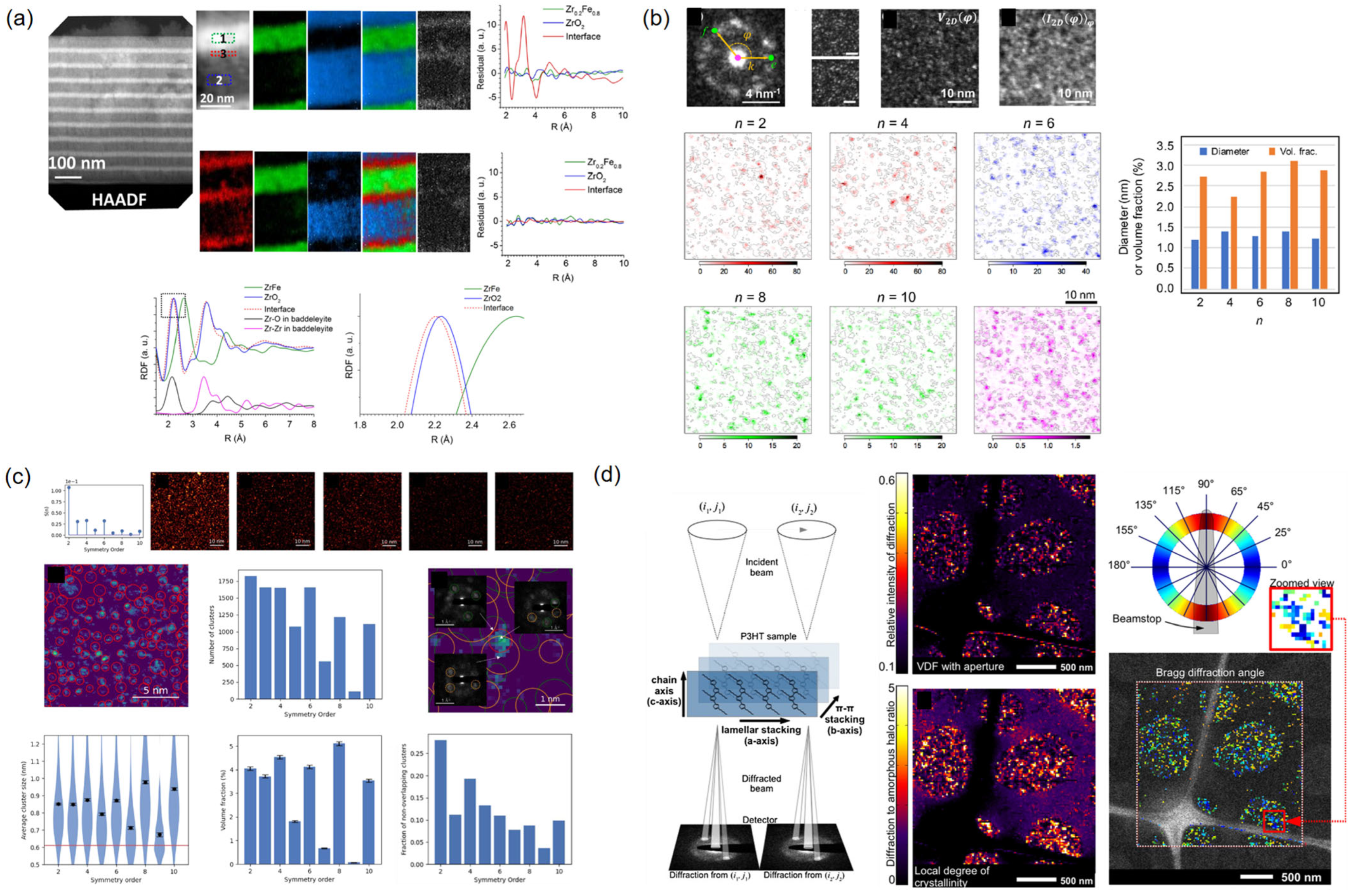
The broad ring patterns in amorphous materials arise from the structure factor of atomic clusters, indicating the preference for specific bond characteristics, representing short-range order. According to kinematic scattering theory, the structure factor can be obtained from the diffraction intensity profile, and the RDF can be derived from the structure factor. RDF extraction relies on kinematic scattering theory, assuming a single scattering event, thus requiring very thin TEM specimens to avoid multiple or dynamical scattering effects in electron diffraction [49]. The post-processing of the diffraction intensity profile yields the total reduced RDF. In elemental amorphous materials, this total reduced RDF corresponds to the real RDF. However, in multi-elemental alloys, the relationship between the total reduced RDF and the real RDF is more complex [49]. Nonetheless, the total reduced RDF is frequently used to analyze short-range order in multi-elemental amorphous materials, offering valuable insights into their structures. Mu, X. et al. demonstrated the feasibility of position-dependent RDF analysis through SED with a nanoscale electron beam for amorphous ZrFe/ZrO2 multilayers [54] (Figure 5a). They also employed this approach to confirm that Cu and Zr tend to induce clustering within the shear band of Zr52.5Cu17.9Ni14.6Al10Ti5 metallic glass [55].
In addition to short-range order, amorphous and glassy materials exhibit significant degrees of structural ordering beyond the first few atomic shells, termed medium-range order. When atomic clusters deviate from complete randomness, Bragg scattering generates speckles within the amorphous halos. Adjusting the size of the electron probe to match the atomic clusters results in increased variation in diffraction patterns, enabling the determination of the degree of medium-range order [51]. This method, known as fluctuation electron microscopy (FEM), also allows the estimation of the density of atomic clusters with different rotational symmetries, known as the angular correlation function, using the FEM dataset. Im, S. et al. conducted FEM analysis using the SED dataset, revealing diverse forms of local ordering within Zr55Co25Al20 metallic glass [56] (Figure 5b). Their work demonstrates the ability to assess details of local structural heterogeneity at the nanometer to mesoscopic scale. Huang, S. et al. proposed averaging correlations at characteristic angles of rotational symmetry, yielding the symmetry coefficient [57] (Figure 5c). They further demonstrated the mapping of rotational symmetry in Pd77.5Cu6Si16.5 metallic glass using SED data by reconstructing symmetry coefficients in two dimensions.
Amorphous materials exhibit broad ring patterns in electron diffractions, with the radius determined by a characteristic scattering length. Analogous to crystalline materials, variations in average atomic spacing, termed strain, induce changes in the radius of these amorphous ring patterns. By employing an elliptical fitting method within SED data and generating two-dimensional maps, the radii of the amorphous rings can be reconstructed, revealing the atomic spacing map influenced by local strain. Gammer, C. et al. utilized this approach to map local elastic strains during the in situ tensile deformation of a Cu36Zr48Al8Ag8 metallic glass [58]. They observed an increase in elastic strain along the tensile direction during loading and noted that the residual elastic strain following fracture gradually diminishes over time.
Figure 5.
SED using a nanoscale electron probe for amorphous and glassy materials. (a) Radial distribution function (RDF) mapping using SED, from Mu, X. et al. (2016). (Reprinted with permission from Ref. [54]. Copyright 2016 Elsevier). (b) Fluctuation electron microscopy (FEM) analysis using SED, from Im, S. et al. (2018). (Reprinted with permission from Ref. [56]. Copyright 2018 Elsevier). (c) FEM-based symmetry mapping using SED, from Huang, S. et al. (2022). (Reprinted with permission from Ref. [57]. Copyright 2022 Elsevier). (d) Crystallinity and orientation mapping of a P3HT-PS polymer sample, from Panova, O. et al. (2016). (Reprinted with permission from Ref. [59]. Copyright 2016 Elsevier).

Numerous functional materials are sensitive to electron beams, precluding atomic-scale imaging and spectroscopies. SED with a nanoscale electron probe presents a solution for examining their atomic structures while mitigating radiation damage. Key to this approach is controlling the dose rate. Various strategies, such as reducing the convergence angle (enlarging the real space probe size), lowering the electron gun current, and defocusing the electron probe, can be employed. Panova, O. et al. mapped the degree of crystallinity and orientation of a polymer sample (50:50 w/w mixture of semicrystalline poly(3-hexylthiophene-2,5-diyl) (P3HT) and amorphous polystyrene (PS)) with a spatial resolution of 20 nm over a field of view of about 1 μm [59] (Figure 5d). Although 20 nm falls short of the high spatial resolution achieved by atomic-scale STEM or HRTEM, it still surpasses the resolution of other imaging techniques. They also characterized the orientation of π–π stacking across a broad field of view in a polymer thin film (poly[2,5-bis(3-tetradecylthiophen-2-yl)thieno[3,2-b]thiophene] (PBTTT)), revealing the coexistence of sharp grain boundaries, overlapping grains, and a liquid crystal-like structure within the polymer [60].
While traditional materials like ceramics, silicon-based semiconductors, and metals have been extensively studied and are typically resistant to electron beam damage, newer materials such as low-dimensional or amorphous semiconductors, quantum materials, perovskite solar cells, and organic–inorganic hybrid materials, currently of interest, tend to be softer and highly sensitive to electron radiation. In this regard, the flexibility to control the dose rate is crucial as it enables the analysis of radiation-sensitive materials. We therefore believe integrating SED with ultrafast electron detectors to characterize radiation-sensitive materials will have a significant impact, potentially leading to breakthroughs that revolutionize upcoming energy and information technologies.
4. Conclusions
The resurgence of interest in SED, also referred to as 4D-STEM in other articles, is propelled by the development of ultrafast electron detectors, advancements in computational power, and the evolution of machine learning algorithms. SED techniques offer versatile approaches for material characterization, depending on the size of the electron probe. With atomic-scale electron probes, SED achieves the highest spatial resolution among diffraction techniques, enabling the analysis of local thickness, symmetry (including octahedral tilt and polarity), and crystal stoichiometry at the unit cell and atomic column levels. Overcoming interference between overlapping CBED disks through position averaging is crucial in SED with atomic-scale probes. On the other hand, nanoscale electron probes enable SED for phase and orientation mapping, strain measurements, symmetry (or polarity) assessments, and the structural analysis of amorphous materials. The ability to control the electron beam dose facilitates the analysis of radiation-sensitive materials at the nanometer scale. Given the large size and complex nature of SED datasets, the adoption of deep learning techniques has consistently proven beneficial across all SED applications. Integrating SED with advanced hardware and artificial intelligence holds promise for establishing robust structure–property relationships, potentially driving groundbreaking discoveries to revolutionize energy and information technologies.
Funding
This work was supported by the National Research Foundation of Korea (NRF) grant funded by the Korean government (MSIT) (No. NRF-2022R1F1A1072330). This work was supported by the Gachon University research fund of 2021 (GCU-202110340001).
Data Availability Statement
Not applicable.
Acknowledgments
The author thanks Sang Woon Hwang and Janghyun Jo for their fruitful discussion.
Conflicts of Interest
The authors declare no conflict of interest.
Appendix A
Figure A1.
Impact of spherical aberration correction on electron probe formation. The contributions to electron probes in conventional STEM (left) and Cs-corrected STEM (right) are compared. Advancements in spherical aberration correction lead to larger optimal convergence angles (α), enabling the formation of atomic-scale electron probes. The Cs values for conventional STEM and Cs-corrected STEM are 1.0 and 0.005 mm, respectively.

References
- Cowley, J. Electron nanodiffraction. Microsc. Res. Tech. 1999, 46, 75–97. [Google Scholar] [CrossRef]
- Ophus, C. Four-dimensional scanning transmission electron microscopy (4D-STEM): From scanning nanodiffraction to ptychography and beyond. Microsc. Microanal. 2019, 25, 563–582. [Google Scholar] [CrossRef]
- Ophus, C. Quantitative Scanning Transmission Electron Microscopy for Materials Science: Imaging, Diffraction, Spectroscopy, and Tomography. Annu. Rev. Mater. Res. 2023, 53, 105–141. [Google Scholar] [CrossRef]
- Levin, B.D. Direct detectors and their applications in electron microscopy for materials science. J. Phys. Mater. 2021, 4, 042005. [Google Scholar] [CrossRef]
- Caswell, T.A.; Ercius, P.; Tate, M.W.; Ercan, A.; Gruner, S.M.; Muller, D.A. A high-speed area detector for novel imaging techniques in a scanning transmission electron microscope. Ultramicroscopy 2009, 109, 304–311. [Google Scholar] [CrossRef]
- Milazzo, A.-C.; Leblanc, P.; Duttweiler, F.; Jin, L.; Bouwer, J.C.; Peltier, S.; Ellisman, M.; Bieser, F.; Matis, H.S.; Wieman, H. Active pixel sensor array as a detector for electron microscopy. Ultramicroscopy 2005, 104, 152–159. [Google Scholar] [CrossRef]
- Tate, M.W.; Purohit, P.; Chamberlain, D.; Nguyen, K.X.; Hovden, R.; Chang, C.S.; Deb, P.; Turgut, E.; Heron, J.T.; Schlom, D.G. High dynamic range pixel array detector for scanning transmission electron microscopy. Microsc. Microanal. 2016, 22, 237–249. [Google Scholar] [CrossRef]
- McMullan, G.; Faruqi, A.; Clare, D.; Henderson, R. Comparison of optimal performance at 300 keV of three direct electron detectors for use in low dose electron microscopy. Ultramicroscopy 2014, 147, 156–163. [Google Scholar] [CrossRef]
- Hachtel, J.A.; Idrobo, J.C.; Chi, M. Sub-Ångstrom electric field measurements on a universal detector in a scanning transmission electron microscope. Adv. Struct. Chem. Imaging 2018, 4, 10. [Google Scholar] [CrossRef]
- Lazić, I.; Bosch, E.G.; Lazar, S. Phase contrast STEM for thin samples: Integrated differential phase contrast. Ultramicroscopy 2016, 160, 265–280. [Google Scholar] [CrossRef]
- Fang, S.; Wen, Y.; Allen, C.S.; Ophus, C.; Han, G.G.; Kirkland, A.I.; Kaxiras, E.; Warner, J.H. Atomic electrostatic maps of 1D channels in 2D semiconductors using 4D scanning transmission electron microscopy. Nat. Commun. 2019, 10, 1127. [Google Scholar] [CrossRef] [PubMed]
- Krajnak, M.; Etheridge, J. A symmetry-derived mechanism for atomic resolution imaging. Proc. Natl. Acad. Sci. USA 2020, 117, 27805–27810. [Google Scholar] [CrossRef]
- Spence, J.; Cowley, J. Lattice imaging in STEM. Optik 1978, 50, 129–142. [Google Scholar]
- Zuo, J.M.; Spence, J.C. Advanced Transmission Electron Microscopy; Springer: Berlin/Heidelberg, Germany, 2017. [Google Scholar]
- Ganesh, K.; Darbal, A.; Rajasekhara, S.; Rohrer, G.; Barmak, K.; Ferreira, P. Effect of downscaling nano-copper interconnects on the microstructure revealed by high resolution TEM-orientation-mapping. Nanotechnology 2012, 23, 135702. [Google Scholar] [CrossRef]
- Kim, K.-H.; Xing, H.; Zuo, J.-M.; Zhang, P.; Wang, H. TEM based high resolution and low-dose scanning electron nanodiffraction technique for nanostructure imaging and analysis. Micron 2015, 71, 39–45. [Google Scholar] [CrossRef]
- Kalinin, S.V.; Ophus, C.; Voyles, P.M.; Erni, R.; Kepaptsoglou, D.; Grillo, V.; Lupini, A.R.; Oxley, M.P.; Schwenker, E.; Chan, M.K. Machine learning in scanning transmission electron microscopy. Nat. Rev. Methods Primers 2022, 2, 11. [Google Scholar] [CrossRef]
- Erni, R. Aberration-Corrected Imaging in Transmission Electron Microscopy: An Introduction; World Scientific Publishing Company: Singapore, 2015. [Google Scholar]
- Nellist, P.D.; Chisholm, M.F.; Dellby, N.; Krivanek, O.; Murfitt, M.; Szilagyi, Z.; Lupini, A.R.; Borisevich, A.; Sides, W., Jr.; Pennycook, S. Direct sub-angstrom imaging of a crystal lattice. Science 2004, 305, 1741. [Google Scholar] [CrossRef]
- Krivanek, O.L.; Chisholm, M.F.; Nicolosi, V.; Pennycook, T.J.; Corbin, G.J.; Dellby, N.; Murfitt, M.F.; Own, C.S.; Szilagyi, Z.S.; Oxley, M.P. Atom-by-atom structural and chemical analysis by annular dark-field electron microscopy. Nature 2010, 464, 571–574. [Google Scholar] [CrossRef]
- Yoon, S.; Gao, X.; Ok, J.M.; Liao, Z.; Han, M.-G.; Zhu, Y.; Ganesh, P.; Chisholm, M.F.; Choi, W.S.; Lee, H.N. Strain-induced atomic-scale building blocks for ferromagnetism in epitaxial LaCoO3. Nano Lett. 2021, 21, 4006–4012. [Google Scholar] [CrossRef]
- Yoo, H.; Yoon, S.; Chung, K.; Kang, S.-H.; Kwon, Y.-K.; Yi, G.-C.; Kim, M. Understanding luminescence properties of grain boundaries in GaN thin films and their atomistic origin. Appl. Phys. Lett. 2018, 112, 131901. [Google Scholar] [CrossRef]
- Yoon, S.; Seo, H.; Jin, K.; Kim, H.G.; Lee, S.-Y.; Jo, J.; Cho, K.H.; Ryu, J.; Yoon, A.; Kim, Y.-W. Atomic Reconstruction and Oxygen Evolution Reaction of Mn3O4 Nanoparticles. J. Phys. Chem. Lett. 2022, 13, 8336–8343. [Google Scholar] [CrossRef]
- LeBeau, J.M.; Findlay, S.D.; Allen, L.J.; Stemmer, S. Position averaged convergent beam electron diffraction: Theory and applications. Ultramicroscopy 2010, 110, 118–125. [Google Scholar] [CrossRef] [PubMed]
- Hwang, J.; Zhang, J.Y.; Son, J.; Stemmer, S. Nanoscale quantification of octahedral tilts in perovskite films. Appl. Phys. Lett. 2012, 100, 191909. [Google Scholar] [CrossRef]
- Ophus, C.; Ercius, P.; Huijben, M.; Ciston, J. Non-spectroscopic composition measurements of SrTiO3-La0.7Sr0.3MnO3 multilayers using scanning convergent beam electron diffraction. Appl. Phys. Lett. 2017, 110, 063102. [Google Scholar] [CrossRef]
- Xu, W.; LeBeau, J.M. A deep convolutional neural network to analyze position averaged convergent beam electron diffraction patterns. Ultramicroscopy 2018, 188, 59–69. [Google Scholar] [CrossRef] [PubMed]
- Kim, Y.H.; Yang, S.H.; Jeong, M.; Jung, M.H.; Yang, D.; Lee, H.; Moon, T.; Heo, J.; Jeong, H.Y.; Lee, E. Hybrid Deep Learning Crystallographic Mapping of Polymorphic Phases in Polycrystalline Hf0.5Zr0.5O2 Thin Films. Small 2022, 18, 2107620. [Google Scholar] [CrossRef]
- Zhang, C.; Feng, J.; DaCosta, L.R.; Voyles, P.M. Atomic resolution convergent beam electron diffraction analysis using convolutional neural networks. Ultramicroscopy 2020, 210, 112921. [Google Scholar] [CrossRef]
- Vincent, R.; Midgley, P. Double conical beam-rocking system for measurement of integrated electron diffraction intensities. Ultramicroscopy 1994, 53, 271–282. [Google Scholar] [CrossRef]
- Palatinus, L.; Jacob, D.; Cuvillier, P.; Klementová, M.; Sinkler, W.; Marks, L.D. Structure refinement from precession electron diffraction data. Acta Crystallogr. Sect. A Found Crystallogr. 2013, 69, 171–188. [Google Scholar] [CrossRef]
- Sunde, J.K.; Marioara, C.D.; van Helvoort, A.T.; Holmestad, R. The evolution of precipitate crystal structures in an Al-Mg-Si (-Cu) alloy studied by a combined HAADF-STEM and SPED approach. Mater. Charact. 2018, 142, 458–469. [Google Scholar] [CrossRef]
- Yuan, R.; Zhang, J.; He, L.; Zuo, J.-M. Training artificial neural networks for precision orientation and strain mapping using 4D electron diffraction datasets. Ultramicroscopy 2021, 231, 113256. [Google Scholar] [CrossRef]
- Rouviere, J.-L.; Sarigiannidou, E. Theoretical discussions on the geometrical phase analysis. Ultramicroscopy 2005, 106, 1–17. [Google Scholar] [CrossRef]
- Galindo, P.L.; Kret, S.; Sanchez, A.M.; Laval, J.Y.; Yáñez, A.; Pizarro, J.; Guerrero, E.; Ben, T.; Molina, S.I. The Peak Pairs algorithm for strain mapping from HRTEM images. Ultramicroscopy 2007, 107, 1186–1193. [Google Scholar] [CrossRef]
- Hÿtch, M.; Houdellier, F.; Hüe, F.; Snoeck, E. Nanoscale holographic interferometry for strain measurements in electronic devices. Nature 2008, 453, 1086–1089. [Google Scholar] [CrossRef]
- Rouviere, J.-L.; Béché, A.; Martin, Y.; Denneulin, T.; Cooper, D. Improved strain precision with high spatial resolution using nanobeam precession electron diffraction. Appl. Phys. Lett. 2013, 103, 241913. [Google Scholar] [CrossRef]
- Zuo, J. Automated lattice parameter measurement from HOLZ lines and their use for the measurement of oxygen content in YBa2Cu3O7-δ from nanometer-sized region. Ultramicroscopy 1992, 41, 211–223. [Google Scholar] [CrossRef]
- Zuo, J.; Kim, M.; Holmestad, R. A new approach to lattice parameter measurements using dynamic electron diffraction and pattern matching. Microscopy 1998, 47, 121–127. [Google Scholar] [CrossRef]
- Ozdol, V.B.; Gammer, C.; Jin, X.G.; Ercius, P.; Ophus, C.; Ciston, J.; Minor, A.M. Strain mapping at nanometer resolution using advanced nano-beam electron diffraction. Appl. Phys. Lett. 2015, 106, 253107. [Google Scholar] [CrossRef]
- Han, Y.M.; Nguyen, K.; Cao, M.; Cueva, P.; Xie, S.E.; Tate, M.W.; Purohit, P.; Gruner, S.M.; Park, J.; Muller, D.A. Strain Mapping of Two-Dimensional Heterostructures with Subpicometer Precision. Nano Lett. 2018, 18, 3746–3751. [Google Scholar] [CrossRef] [PubMed]
- Gammer, C.; Kacher, J.; Czarnik, C.; Warren, O.L.; Ciston, J.; Minor, A.M. Local and transient nanoscale strain mapping during in situ deformation. Appl. Phys. Lett. 2016, 109, 081906. [Google Scholar] [CrossRef]
- Tsuda, K.; Yasuhara, A.; Tanaka, M. Two-dimensional mapping of polarizations of rhombohedral nanostructures in the tetragonal phase of BaTiO3 by the combined use of the scanning transmission electron microscopy and convergent-beam electron diffraction methods. Appl. Phys. Lett. 2013, 103, 082908. [Google Scholar] [CrossRef]
- Tsuda, K.; Tanaka, M. Nanometer-scale local structural study of the paraelectric cubic phase of KNbO3 by convergent-beam electron diffraction. Jpn. J. Appl. Phys. 2017, 56, 10PB09. [Google Scholar] [CrossRef]
- Morikawa, D.; Tsuda, K. Local crystal symmetry and structure at CaTiO3 twin boundaries. Appl. Phys. Lett. 2021, 118, 092901. [Google Scholar] [CrossRef]
- Kim, K.H.; Payne, D.A.; Zuo, J.M. Determination of 60° polarization nanodomains in a relaxor-based ferroelectric single crystal. Appl. Phys. Lett. 2015, 107, 162902. [Google Scholar] [CrossRef]
- Shao, Y.T.; Zuo, J.M. Lattice-Rotation Vortex at the Charged Monoclinic Domain Boundary in a Relaxor Ferroelectric Crystal. Phys. Rev. Lett. 2017, 118, 157601. [Google Scholar] [CrossRef] [PubMed]
- Shao, Y.T.; Zuo, J.M. Nanoscale symmetry fluctuations in ferroelectric barium titanate, BaTiO3. Acta Crystallogr. Sect. B-Struct. Sci. Cryst. Eng. Mater. 2017, 73, 708–714. [Google Scholar] [CrossRef]
- Cockayne, D.J.H. The study of nanovolumes of amorphous materials using electron scattering. Annu. Rev. Mater. Res. 2007, 37, 159–187. [Google Scholar] [CrossRef]
- Mitchell, D.R.G.; Petersen, T.C. RDFTools: A software tool for quantifying short-range ordering in amorphous materials. Microsc. Res. Tech. 2012, 75, 153–163. [Google Scholar] [CrossRef] [PubMed]
- Hwang, J.; Voyles, P.M. Variable Resolution Fluctuation Electron Microscopy on Cu-Zr Metallic Glass Using a Wide Range of Coherent STEM Probe Size. Microsc. Microanal. 2011, 17, 67–74. [Google Scholar] [CrossRef]
- Gibson, J.M.; Treacy, M.M.J.; Sun, T.; Zaluzec, N.J. Substantial Crystalline Topology in Amorphous Silicon. Phys. Rev. Lett. 2010, 105, 125504. [Google Scholar] [CrossRef]
- Ebner, C.; Sarkar, R.; Rajagopalan, J.; Rentenberger, C. Local, atomic-level elastic strain measurements of metallic glass thin films by electron diffraction. Ultramicroscopy 2016, 165, 51–58. [Google Scholar] [CrossRef]
- Mu, X.K.; Wang, D.; Feng, T.; Kübel, C. Radial distribution function imaging by STEM diffraction: Phase mapping and analysis of heterogeneous nanostructured glasses. Ultramicroscopy 2016, 168, 1–6. [Google Scholar] [CrossRef]
- Mu, X.K.; Chellali, M.R.; Boltynjuk, E.; Gunderov, D.; Valiev, R.Z.; Hahn, H.; Kübel, C.; Ivanisenko, Y.; Velasco, L. Unveiling the Local Atomic Arrangements in the Shear Band Regions of Metallic Glass. Adv. Mater. 2021, 33, 2007267. [Google Scholar] [CrossRef] [PubMed]
- Im, S.; Chen, Z.; Johnson, J.M.; Zhao, P.Y.; Yoo, G.H.; Park, E.S.; Wang, Y.Z.; Muller, D.A.; Hwang, J. Direct determination of structural heterogeneity in metallic glasses using four-dimensional scanning transmission electron microscopy. Ultramicroscopy 2018, 195, 189–193. [Google Scholar] [CrossRef] [PubMed]
- Huang, S.Y.; Francis, C.; Sunderland, J.; Jambur, V.; Szlufarska, I.; Voyles, P.M. Large Area, High Resolution Mapping of Approximate Rotational Symmetries in a Pd77.5Cu6Si16.5 Metallic Glass Thin Film. Ultramicroscopy 2022, 241, 113612. [Google Scholar] [CrossRef] [PubMed]
- Gammer, C.; Ophus, C.; Pekin, T.C.; Eckert, J.; Minor, A.M. Local nanoscale strain mapping of a metallic glass during in situ testing. Appl. Phys. Lett. 2018, 112, 171905. [Google Scholar] [CrossRef]
- Panova, O.; Chen, X.C.; Bustillo, K.C.; Ophus, C.; Bhatt, M.P.; Balsara, N.; Minor, A.M. Orientation mapping of semicrystalline polymers using scanning electron nanobeam diffraction. Micron 2016, 88, 30–36. [Google Scholar] [CrossRef] [PubMed]
- Panova, O.; Ophus, C.; Takacs, C.J.; Bustillo, K.C.; Balhorn, L.; Salleo, A.; Balsara, N.; Minor, A.M. Diffraction imaging of nanocrystalline structures in organic semiconductor molecular thin films. Nat. Mater. 2019, 18, 860–865. [Google Scholar] [CrossRef]
Figure 1.
Schematic representation of scanning electron diffraction (SED), also known as four-dimensional scanning electron microscopy (4D-STEM). SED captures electron diffraction data for every position scanned by the electron probe. The gray points on the specimen mark the position of electron probe, with the arrow showing its movement.

Figure 2.
Formation of the electron probe and convergence angle (α). (a) Impact of diffraction limit, spherical aberration, chromatic aberration, and source size on probe radius. Each factor has its specific dependency on the convergence angle. (b) Relationship between convergence angle and probe radius. A convergence angle of α > 30 is necessary to achieve atomic-scale electron probe.

Disclaimer/Publisher’s Note: The statements, opinions and data contained in all publications are solely those of the individual author(s) and contributor(s) and not of MDPI and/or the editor(s). MDPI and/or the editor(s) disclaim responsibility for any injury to people or property resulting from any ideas, methods, instructions or products referred to in the content. |
© 2024 by the author. Licensee MDPI, Basel, Switzerland. This article is an open access article distributed under the terms and conditions of the Creative Commons Attribution (CC BY) license (https://creativecommons.org/licenses/by/4.0/).
Share and Cite
MDPI and ACS Style
Yoon, S. Decoding Material Structures with Scanning Electron Diffraction Techniques. Crystals 2024, 14, 275. https://doi.org/10.3390/cryst14030275
AMA Style
Yoon S. Decoding Material Structures with Scanning Electron Diffraction Techniques. Crystals. 2024; 14(3):275. https://doi.org/10.3390/cryst14030275
Chicago/Turabian StyleYoon, Sangmoon. 2024. "Decoding Material Structures with Scanning Electron Diffraction Techniques" Crystals 14, no. 3: 275. https://doi.org/10.3390/cryst14030275
Note that from the first issue of 2016, this journal uses article numbers instead of page numbers. See further details here.