Article

Anion Doping of Tungsten Oxide with Nitrogen: Reactive Magnetron Synthesis, Crystal Structure, Valence Composition, and Optical Properties

by
Insaf F. Malikov
1,2,
Nikolay M. Lyadov
1,
Myakzyum K. Salakhov
2 and
Lenar R. Tagirov
1,*
1
Zavoisky Physical-Technical Institute, FRC KazSC of RAS, Kazan 420029, Russia
2
Institute of Physics, Kazan Federal University, Kazan 420008, Russia
*
Author to whom correspondence should be addressed.
Crystals 2024, 14(2), 109; https://doi.org/10.3390/cryst14020109
Submission received: 27 November 2023 / Revised: 29 December 2023 / Accepted: 16 January 2024 / Published: 23 January 2024
(This article belongs to the Special Issue Feature Papers in Crystals 2023)

Abstract

:
Anion doping of tungsten trioxide by nitrogen is used to obtain electrochrome cathode materials, the spectral transmittance of which can be controlled by the doping level. A series of samples was synthesized by reactive magnetron sputtering of a metal tungsten target in a mixture of argon, nitrogen, and oxygen gases, the flow rate of the latter was varied at a constant pressure of the gas mixture. Warm-colored tungsten oxynitride films were prepared at higher doping levels with their morphology and elemental composition characterized using scanning electron microscopy, crystal structure described using X-ray diffraction and the valence state of constituents revealed with X-ray photoelectron spectroscopy techniques. Optical properties were measured by making use of transmission spectrophotometry and spectroscopic ellipsometry. These extensive experimental studies revealed an increase in absorption towards shorter wavelengths below the wavelength of 0.5 µm with an increase in the doping level. At the same time, it was found that with an increase in the doping level, partial reduction of the tungsten occurs, and the fraction of non-stoichiometric oxygen steadily increases to half of the total oxygen content. It is a common belief that the imperfection of the doped material facilitates the intercalation of the material by electrolyte ions.

1. Introduction

Electrochromism of inorganic oxide materials is a phenomenon in which the transparency as well as the color of the material change due to the reversible ion intercalation under the influence of an applied voltage (see [1,2,3,4,5,6,7,8] and references therein). This phenomenon has been known for a long time [9] and has prospects for use in architectural glazing, interior design, and the automotive industry (see [10,11,12,13,14,15,16,17] and references therein); however, it has not yet found mass application, since electrochromic products require long-term stability of many parameters in sometimes harsh operating conditions: high and low temperatures with large gradients, intense exposure to direct sunlight for a long time, etc. Therefore, electrochromic glass is more or less regularly used in the form of rear-view mirrors inside the interior of some brands of cars, window shutters of some aircrafts, etc. There is ongoing work to improve the performance of electrochromic devices, their durability, and the number of switches between the colored and bleached states [17,18,19,20].
Tungsten trioxide WO3 (in general, not fully stoichiometric WO3−x) is one of the known cathode electrochromic materials, the optical density of which changes upon intercalation with protons (H+), alkali metal ions (Li, K), and alkaline earth (Al) metals, which are moieties of the electrolyte of an electrochromic cell (see [1,2,3,4,5] and references therein). It can be fabricated in a thin-film form using several techniques such as chemical vapor deposition, physical vapor deposition including reactive sputtering, cathodic electrodeposition and thermal evaporation, wet chemical synthesis including sol-gel processes, hydrothermal and solvothermal methods, electrochemical deposition, spray pyrolysis, deposition of nanoparticles, mechanical sputtering, etc. (see [1,17,18,19,20,21,22,23,24] and references therein). Regardless of the fabrication route, the resulting WO3−x is an inorganic material that is highly resistant to prolonged exposure to sunlight and high temperatures; however, the transition time from the bleached to the colored state, and vice versa, strongly depends on the method of preparation of tungsten oxide films and can reach several minutes [14,17,18,20,21,24]. In addition, the darkened state is characterized by an intense blue color, which is hardly comfortable to potential users of the electrochromic glass technology.
One of the ways to increase the coloring/bleaching rate and its dynamic range could be to redistribute the voltage drop across the anode/electrolyte/cathode stack in favor of the electrolyte. Since, from a formal point of view, tungsten trioxide is a wide-gap semiconductor, its conductivity can be affected by doping. An additional advantage of doping could be the redistribution of the spectral density of light absorption in relative favor of the short-wavelength (blue) part of the visible spectrum to balance the blue coloration and shift the visual assessment of color towards a neutral one (achromatic). Finally, doping can affect the micro- and nanostructure of the tungsten oxide electrode, thus facilitating the process of intercalation/de-intercalation of ions from the electrolyte. Due to the compound nature of the WOx material, it can be subject to both cationic and/or anionic doping. There are a variety of transition metal ions that can be used for cationic doping to substitute tungsten. On the contrary, there is maybe a unique anionic dopant which concurrently binds to tungsten in the presence of the oxygen. Nitrogen is known to form oxynitride compounds with tungsten [25]. In the thin-film form, nitrogen oxynitride was synthesized in several works [26,27,28,29,30,31,32,33,34], and the crystal structure, electrical, and optical properties were examined. In this work, we use anionic doping by nitrogen to study the micro- and nanostructure of the resulting tungsten oxynitride material with special emphasis on the valence evolution of W ions and the stoichiometry of their oxygen environment.

2. Materials and Methods

Thin films of tungsten oxynitride (WOxNy = WON) were grown by reactive magnetron sputtering in an atmosphere of a high-purity reactive plasma gas consisting of argon (plasma-forming gas, flow rate in the range of 80–86 sccm, see Table 1), nitrogen (reactive gas, flow rate 50 sccm), and oxygen (reactive gas, flow rate in the range 4–10 sccm, see Table 1), guided using a computer via precision gas-flow leakers with an accuracy of 0.1%. The total flow rate of argon and oxygen for each sample was 90 sccm. The pressure in the chamber was automatically maintained at 4 Pa (30 mTorr) using a digital throttle valve throughout the entire deposition cycle. Despite the constant nitrogen flow rate, oxygen, being chemically much more reactive than nitrogen, gradually replaces nitrogen in the resulting compound upon increasing the oxygen flow rate.
Sputtering took place from a metal target of high purity tungsten (99.9% of W), the power supplied to the magnetron was automatically maintained at a constant level of 300 W. The substrate for deposition was a polished double-sided glass slide for microscopic studies with a size of 75 × 25 mm2 and a thickness of 1 mm, pre-cleaned in an aqueous solution of sodium alkylbenzenesulfonate, tetrasodium EDTA, and sodium pyrophosphate using an ultrasonic bath. The nomenclature of the synthesized samples is as follows (see Table 1): sample #111 was obtained at an oxygen flow rate of 4 sccm; #092—with a flow rate of 6 sccm; #091—with a flow rate of 7 sccm; #082—with a flow rate of 10 sccm; annealed samples are marked by the suffix “t”, for example #082t.
After evacuating the prepared films from the vacuum chamber, they were cut into several parts for further studies; in particular, one fragment of each initial sample was collected in an alumina tray and annealed in a muffle furnace in an air atmosphere according to the cyclogram: 2 h heating from room temperature to 673 K (400 °C), then annealing for 10 h at 673 K, and cooling for 4 h to room temperature.
The morphology of the resulting films was examined using a Carl Zeiss Merlin scanning electron microscope (SEM) (ZEISS Group, Oberkochen, Germany), while the elemental analysis was carried out using an Oxford Inca energy dispersive X-ray unit (EDX) and a Carl Zeiss EVO50 XVP (Carl Zeiss AG, Oberkochen, Germany) scanning electron microscope.
X-ray diffraction (XRD) analysis was performed on a Rigaku SmartLab diffractometer (Rigaku Corporation, Tokyo, Japan) with the Cu Kα1 radiation (λ = 1.5059 Å) in the Bragg–Brentano geometry; the beam incidence angle was 0.3°, the angular step was 0.02°, and the scanning speed was 2 s per point; range of angles 2θ from 10° to 60°. The diffraction pattern was processed using the built-in PDXL 2 software (version 2.0.3.0) and the ICDD PDF-2 crystalline compound database.
The near-surface elemental composition and the valence states of constituents were studied by X-ray photoelectron spectroscopy (XPS). The XPS setup operates at a base pressure of 3 × 10⁻⁸ Pa, it is equipped with a Mg-Kα X-ray source operating at 12.5 kV and 250 W, and a Phoibos 150 hemispherical energy analyzer of photoelectrons (all from SPECS, Berlin, Germany). Survey XPS spectra were recorded in the range of 0–1000 eV with an energy step of 1 eV and a pass energy of 80 eV. High-resolution spectra were recorded in limited energy ranges of interest with an average of over 100 scans for all elements, an energy step of 0.1 eV, and the pass energy of 20 eV. The setup is also equipped with a built-in option for surface etching with a wide oblique beam of argon ions of variable energy for depth profiling [35,36].
The optical properties of WON were studied using a PerkinElmer Lambda 1050 UV/VIS/NIR spectrophotometer (PerkinElmer, Waltham, MA, USA) in the visible wavelength range of 0.38–0.78 μm in transmission geometry. For a more detailed analysis of optical attenuation and refraction, a spectroscopic ellipsometry technique (Woollam VASE, J.A. Woollam, Lincoln, NE, USA) was used in the wavelength range of 0.25–2.5 μm in reflection geometry. The measurements were carried out at the angles of incidence of the optical axis of collimated radiation of 55° and 75°.

3. Results

3.1. Scanning Electron Microscopy and X-ray Diffraction (XRD) Analysis

The morphology of the resulting films was examined using a Carl Zeiss Merlin SEM and showed a mesoporous surface structure of the synthesized samples with dimensional features of two scales: the sub-micron one of about 50–100 nm and the predominantly much smaller scale in the range mostly below 30 nm (see Figure 1). Actual distributions of the mesoporous surface features are given in the insets in Figure 1a,d.
X-ray diffraction (XRD) analysis performed using the Rigaku SmartLab diffractometer has shown that the glass substrate, generally being an amorphous material, reveals the presence of a short-range order in the arrangement of atoms (broad feature in the range of angles ~15–38°). The diffraction pattern of the WON film on the substrate after deposition shows a broad peak of amorphous material with a maximum shift towards higher angles compared with the substrate. The broad peak of short-range order in the glass substrate is suppressed due to the absorption of X-ray radiation in the film, and the latter broad absorption is a weighted superposition of the absorptions by the film and the substrate.
Peaks appear in the diffraction pattern of the samples after annealing indicating (partial) the crystallization of the initially amorphous film material. Moreover, the identification of the crystalline phases shows that the glass substrate ions take part in formation of the crystalline phase. In particular, in sample #111t (~240 nm thick film), Figure 1c, the XRD data show the presence of two almost equally weighted crystalline phases, Na2W4O13 (red labels) and Na2W2O7 (green labels), which accounts for a minor portion of the film thickness. A considerable contribution from the amorphous matter indicates this. On the contrary, in sample #082t (~120 nm thick), Figure 1f, the XRD data show the predominant crystalline contribution of the Na2W2O7 phase, which accounts for most of the original amorphous material of the film. The XRD data indicate that crystallization begins at the film/glass substrate interface.
The elemental composition measured by the EDX method has shown the presence of WON film elements, as well as a mixture of Na, Ca, Si, characteristic of the glass substrate. It is obvious that the region of excitation of the characteristic X-ray radiation by electrons at an accelerating voltage of 10 kV also covers a substrate, since the film is thinner (~120–240 nm) than the EDX probing depth of the order of 0.5 μm. Indeed, the third column of Table 2 shows a systematic increase of the oxygen content with a decrease of the film thickness from sample #111 to sample #082. Moreover, the W and O columns under the header “Annealed” clearly indicate a gradual increase in the deviation from the WO3 stoichiometry upon going from the thicker to thinner films. Therefore, the tungsten to oxygen ratio should be treated with caution since the oxygen signal contains a contribution from the substrate (see also a discussion below). Concerning nitrogen content in the as-deposited samples, 4th column of Table 2, it gradually decreases from ~21 at% to ~10 at% when the oxygen flow rate increases from 4 sccm, Table 1, sample #111, to 10 sccm, sample #082. Annealing in air leads to the replacement of nitrogen in the film structure by oxygen: the presence of nitrogen is indicated at a level of 2.6 at.% in sample #111t, see 7th column of Table 2, while for the lower content of nitrogen in the as-deposited samples, #092 to #082, the quantitative definition of nitrogen content is not possible due to the low signal intensity and the overlap of the nitrogen line with the lines of oxygen and calcium.

3.2. X-ray Photoelectron Spectroscopy

The XPS method also makes it possible to estimate the elemental composition of the material being probed; however, the advantage of the XPS method lies in the possibility of determining the valence composition of the material under study. Unlike the EDX method, XPS is intended for surface and near-surface studies, since the probing depth is several nanometers. It is obvious that the substrate does not contribute to the signal from the film with a thickness of 120–240 nm; however, surface contaminations, for example, with carbon dioxide absorbed from air, and the gradual oxidation of the surface at ambient conditions may lead to extrinsic contributions to the XPS signal (see below).
Figure 2 shows the overview XPS spectra of samples #111 and #082, as well as the high-resolution spectra separately for W, O, and N (see the figure caption). The results of the valence analysis are presented element by element in Table 2. The XPS spectrum of tungsten contains one or two doublets with binding energies of 35.8 eV and 37.9 eV, and 34.3 eV and 36.4 eV, respectively. The binding energies of the more intense doublet of 35.8 eV and 37.9 eV in sample #111, Figure 2b, correspond to tungsten in the 6+ valence state [37,38,39], while the binding energies of the less intense doublet are attributed to tungsten in a non-stoichiometric environment (partially reduced) [37,38]. In sample #082, tungsten was found only in the oxidized state 6+ (see Figure 2f). The Shirley-type [40,41] background following the algorithm from CasaXPS [42], was subtracted from each spectrum before calculating the abundance of each component in the spectrum taking into account the photoelectron yield.
The nitrogen lines have a low signal-to-noise ratio; therefore, identification of valence states was not carried out. Due to the small depth of probing, the nitrogen to oxygen signal ratio should be treated critically, since after evacuation from the vacuum chamber, the non-equilibrium oxidized tungsten, located close to the film surface, continues oxidizing by atmospheric oxygen. Due to the shallow probing depth, a sizeable contribution to the oxygen XPS signal is made by near-surface oxygen chemisorbed from the ambient atmosphere, which leads to an overestimation of its content.
To get rid of the surface oxygen signal, we used the built-in option for surface etching with a wide oblique beam of argon ions. To be sure that the etching rate does not depend noticeably on the presence of nitrogen, we etched the #111 sample comparatively with pilot sample #082t, in which tungsten is completely oxidized to a valence of 6+, and the presence of nitrogen is not detected by any methods available to us. As a result, we obtained an almost identical evolution of the W and O XPS spectra for both samples, but the intensity of the nitrogen signal in the #111 sample quickly increased and saturated at a level four times higher than that of the non-etched state. This indeed indicates oxidation of the surface of sample #111.
Additional information can be obtained from the analysis of the oxygen signal line shape, Figure 2c,g, showing the splitting of the XPS line into two components. One of them (with a binding energy of 530.8 eV) is identified as stoichiometric oxygen in the composition of WO3 [37,38], while the other with a binding energy of 532.4 eV is identified as oxygen in the nonstoichiometric tungsten oxide. The analysis of the experimental data for all samples has shown (see Table 3) that in the non-annealed samples the fraction of the non-stoichiometric oxygen (third column of the Table 3) steadily increases with an increase in the nitrogen content.

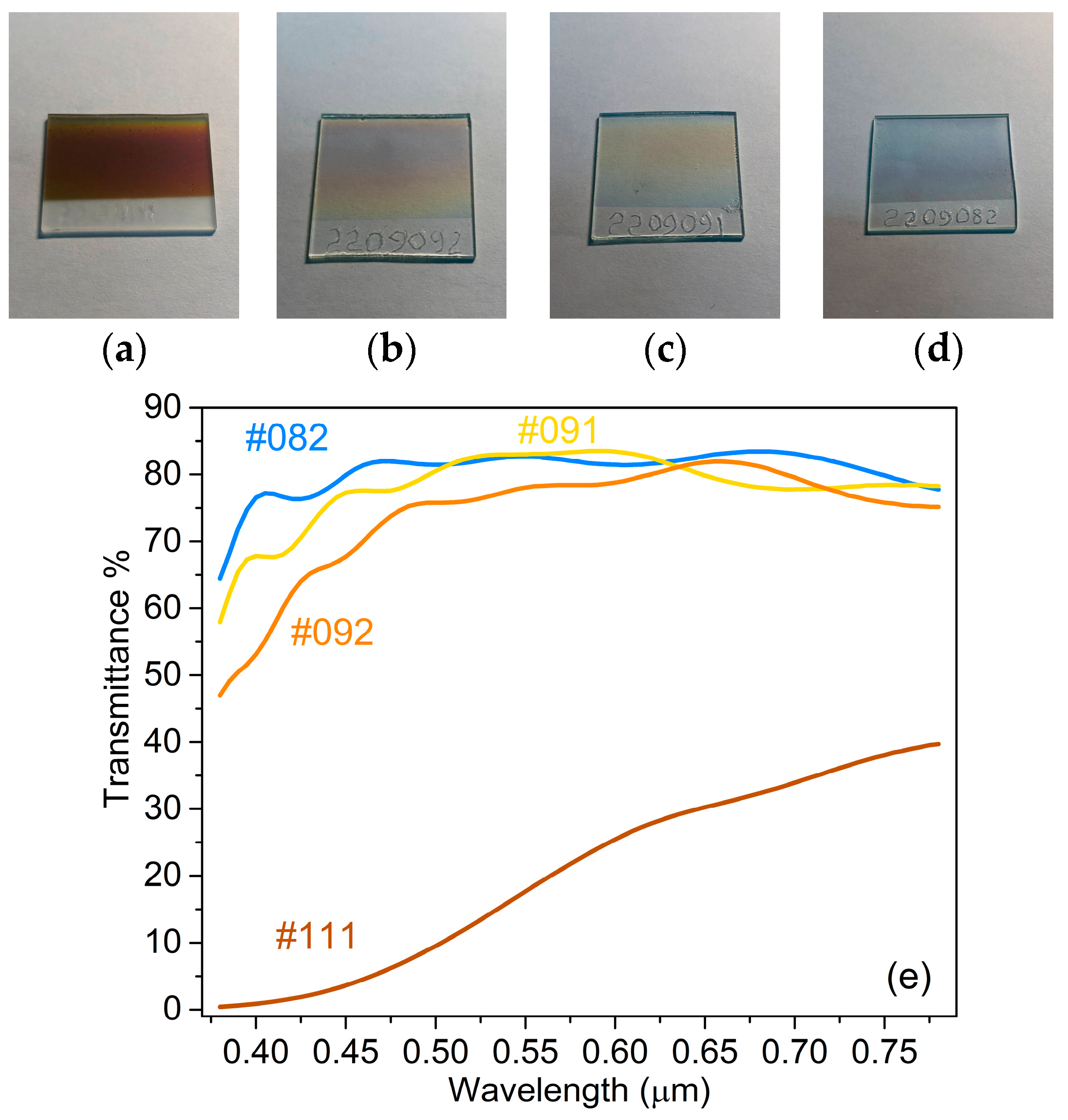
3.3. Spectrophotometric Measurements

Figure 3 shows photographs of the as-deposited samples (top row, (a) to (d) in perceived colors) and the results of the spectroscopic transmission measurements (window €). Visually, sample #111 is brown; sample #092—light beige; sample #091—light yellow; sample #082—transparent with a bluish tint. The integral transmission in the wavelength range of 0.38–0.78 μm is 20.4%, 74.2%, 78.2%, and 80.6% for samples #111, #092, #091, and #082, respectively (see Table 1).
The optical transmission spectrum of the samples is presented in panel (e) of Figure 3. The oscillatory component of the absorption dispersion for samples #082, #091, and #092 originates from the light interference in the thin semi-transparent film. It can be seen that for sample #111, with the maximum nitrogen content, that the transmission is minimal in the short wavelength side; it monotonically increases towards the long wavelengths from almost zero to ~40%. The lack of transmission of blue and green colors leads to the severe darkening of the WON film. Increasing the oxygen flux during the film deposition from 4 to 6 sccm, with a constant nitrogen flux of 50 sccm (see Table 1), leads to sharp changes in the optical transmission, significantly increasing transparency in the short-wavelength part of the spectrum with a rough constant absorption at longer wavelengths. As a result, the intensity of the brown color drops down significantly, turning the film color a light-beige. A further increase in the oxygen flow rate to 7 sccm leads to a color change to yellow, due to an increase in the transmittance in the wavelength range of 0.38–0.635 μm, with approximately the same transmittance at longer wavelengths. Finally, increasing the oxygen flow rate to 10 sccm increases the transmittance in the wavelength range of 0.38–0.505 μm, while approximately maintaining the transmittance at longer wavelengths. It is observed as a blue tint of light transmitted by the sample. Thus, we observe that the anionic doping of tungsten oxide with nitrogen leads to the appearance of a warm coloration of the resulting tungsten oxynitride film.

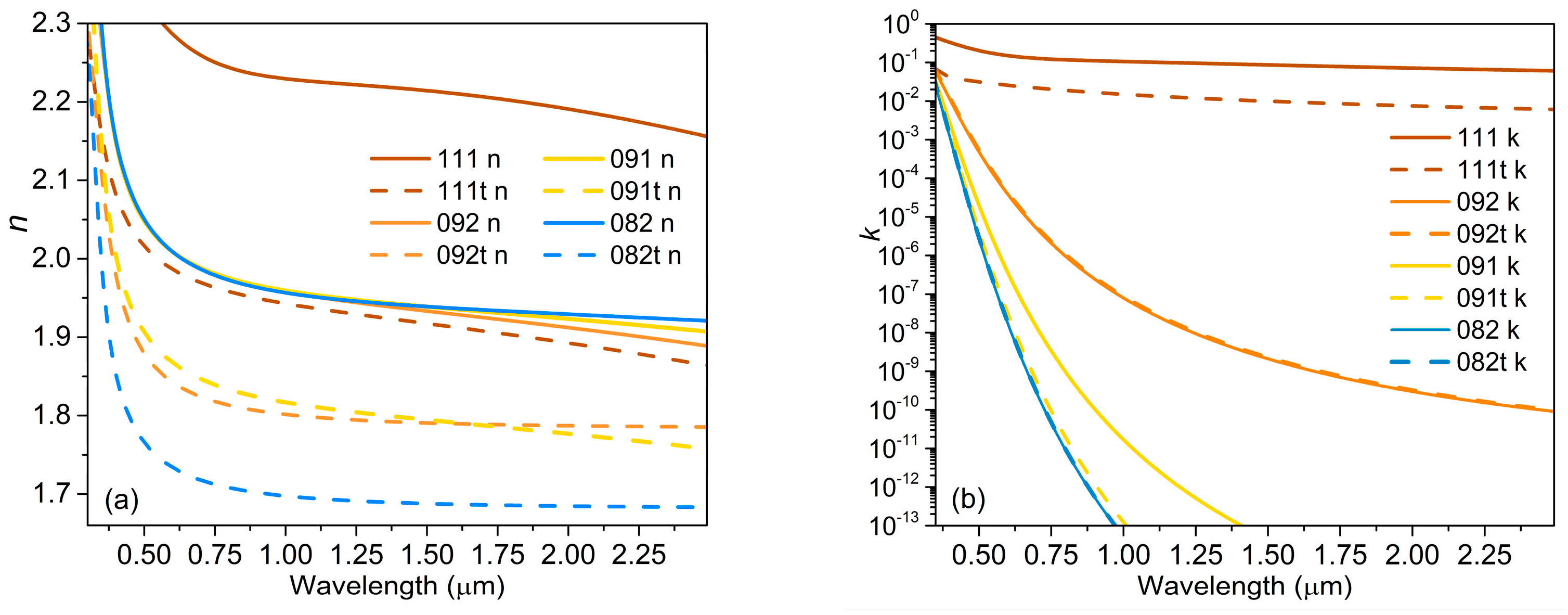
3.4. Spectroscopical Ellipsometry

Extended information about the optical properties of tungsten oxynitride can be obtained from spectrometric ellipsometry measurements in the wavelength range of 0.25–2.5 μm. The measurement results are presented in Figure 4 in the form of the dependence of the refraction n and extinction k coefficients on the wavelength of the incident radiation. They show that the anionic doping with nitrogen leads to a systematic increase in absorption in the short-wavelength region, which leads to the dominance of long waves in transmission, and as a consequence, to the coloration of the nitrogen-doped tungsten oxide layer to warm colors.

4. Discussion

This study considers the anionic doping of the cathode electrochromic material tungsten trioxide by nitrogen. Visually, with an increase in the doping level, the effect of coloring to warm colors was observed—from transparent bluish to brown, through yellow and beige shades. XRD measurements have shown that predominantly amorphous films of tungsten oxynitride were deposited (Figure 1c,f, blue lines) with a broad shoulder in the angle range of 18–38°. It is most likely the reminiscence of the most intense reflections of the WO3 crystalline powder structure [43], generated by the short-range order in the quasi-amorphous film. Upon annealing, the films partially crystallize (Figure 1c,f, red lines) with the appearance of XRD peaks corresponding to the crystalline powder reflections of Na2W4O13 and Na2W2O7 compounds for the thickest #111t sample; and Na2W2O7 compounds for the thinnest #082t sample. The crystalline phases of the #111t sample account for only minority of the total initial film volume, while the crystalline phase of the #082t sample accounts for the majority of the film volume (see red lines in Figure 1c,f). This observation gives a clear hint that crystallization starts from the substrate–film interface. The significantly increased contribution of stoichiometric oxygen to the XPS spectra in all samples upon annealing, see Table 3, two columns in the right, occurs because of nitrogen escape (see Table 2), as well as a general increase in order upon annealing. Ultimately, the annealed films become transparent, which is characteristic of stoichiometric tungsten oxide compounds with the available elements from our samples.
The study of optical properties by transmission spectrophotometry and spectroscopic ellipsometry has shown that anionic doping of tungsten trioxide with nitrogen leads to an increase in absorption at short (UV) wavelengths without noticeable modification at wavelengths above ~0.6 μm, at least up to 2.5 μm, which is the limit of our spectrometers. This short-wavelength absorption causes the material to have warm colors, in contrast to the dark-blue coloration of tungsten trioxide itself upon intercalation with Li.
An intriguing conclusion can be drawn from the systematic increase of the fraction of non-stoichiometric oxygen with the increase in the nitrogen doping level (Table 3, third column). It is known that the amorphous character of WO3−x films, as well as imperfections like oxygen vacancies, enhance coloration efficiency [8,24,44,45]. Therefore, nitrogen-doped tungsten oxide material can color/bleach deeper and faster, opening up directions for improving the consumer properties of electrochemical materials and devices.

Author Contributions

Conceptualization, L.R.T. and M.K.S.; methodology, L.R.T. and M.K.S.; sample preparation, I.F.M.; investigation, I.F.M., N.M.L., M.K.S. and L.R.T.; resources, L.R.T. and M.K.S.; data curation, I.F.M., N.M.L. and L.R.T.; writing—original draft preparation, L.R.T.; writing—review and editing, M.K.S., I.F.M. and N.M.L.; visualization, I.F.M.; supervision, L.R.T.; project administration, L.R.T.; funding acquisition, L.R.T. All authors have read and agreed to the published version of the manuscript.

Funding

The research of I.F.M., N.M.L. and L.R.T. was funded by Russian Science Foundation (RSF), project # 22-22-00980.

Data Availability Statement

Since the original data is completed together with partners who ignited the study of electrochromism, the data presented in this study are available on request from the corresponding author.

Acknowledgments

The authors sincerely thank V. Meshcheryakov, V. Chugunov, M. Yermakov for their valuable support in sample preparation; R. Batulin, A. Gumarov, L. Nurtdinova, A. Rogov, I. Tverdov, I. Vakhitov, and R. Yusupov for their assistance in measurements. X-ray diffraction studies were carried out using the equipment of the Center for Shared Facilities “Nanomaterials and Nanotechnologies” of the Kazan National Research Technological University (KNRTI-KChTI).

Conflicts of Interest

The authors declare no conflict of interest.

References

  1. Granqvist, C.G. Handbook of Inorganic Electrochromic Materials; Elsevier: Amsterdam, The Netherlands, 2002; 663p. [Google Scholar]
  2. Monk, P.M.S.; Mortimer, R.J.; Rosseinsky, D.R. Electrochromism and Electrochromic Devices; Cambridge University Press: Cambridge, UK, 2007; 483p. [Google Scholar]
  3. Niklasson, G.A.; Granqvist, C.G. Electrochromics for smart windows: Thin films of tungsten oxide and nickel oxide, and devices based on these. J. Mater. Chem. 2007, 17, 127–156. [Google Scholar] [CrossRef]
  4. He, T.; Yao, J. Photochromic materials based on tungsten oxide. J. Mater. Chem. 2007, 17, 4547. [Google Scholar] [CrossRef]
  5. Gillaspie, D.T.; Tenent, R.C.; Dillon, A.C. Metal-oxide films for electrochromic applications: Present technology and future directions. J. Mater. Chem. 2010, 20, 9585–9592. [Google Scholar] [CrossRef]
  6. Ma, D.; Wang, J. Inorganic electrochromic materials based on tungsten oxide and nickel oxide nanostructures. Sci. China Chem. 2017, 60, 54–62. [Google Scholar] [CrossRef]
  7. Maiorov, V.A. Electrochromic glasses with separate regulation of transmission of visible light and near-infrared radiation (Review). Opt. Spectrosc. 2019, 126, 412–430. [Google Scholar] [CrossRef]
  8. Li, Z.; Liu, Z.; Zhao, L.; Chen, Y.; Li, J.; Yan, W. Efficient electrochromic efficiency and stability of amorphous/crystalline tungsten oxide film. J. Alloys Comp. 2023, 930, 167405. [Google Scholar] [CrossRef]
  9. Deb, S.K. A novel electrophotographic system. Appl. Opt. 1969, 8, 192–195. [Google Scholar] [CrossRef] [PubMed]
  10. Granqvist, C.G.; Lansaker, P.C.; Mlyuka, N.R.; Niklasson, G.A.; Avendano, E. Progress in chromogenics: New results for electrochromic and thermochromic materials and devices. Sol. Energy Mater. Sol. Cells 2009, 93, 2032–2039. [Google Scholar] [CrossRef]
  11. Granqvist, C.G.; Green, S.; Niklasson, G.A.; Mlyuka, N.R.; Kraemer, S.; Georen, P. Advances in chromogenic materials and devices. Thin Solid Films 2010, 518, 3046–3053. [Google Scholar] [CrossRef]
  12. Granqvist, C.G. Electrochromics and thermochromics: Towards a new paradigm for energy efficient buildings. Mater. Today Proc. 2016, 3, S2–S11. [Google Scholar] [CrossRef]
  13. Shchegolkov, A.V.; Tugolukov, E.N.; Shchegolkov, A.V. Overview of electrochromic materials and devices: Scope and development prospects. Adv. Mater. Technol. 2020, N2, 66–73. [Google Scholar] [CrossRef]
  14. Zhang, W.; Li, H.; Hopmann, E.; Elezzabi, A.Y. Nanostructured inorganic electrochromic materials for light applications. Nanophotonics 2020, 10, 825–850. [Google Scholar] [CrossRef]
  15. Shchegolkov, A.V.; Parfimovich, I.D.; Komarov, F.F.; Shchegolkov, A.-d.V.; Tugolukov, E.N. Optically adjustable nanocomposite electrochromic film WO3/rGO to control light transmission and protect from electromagnetic radiation. Inorg. Mater. Appl. Res. 2021, 12, 1547–1553. [Google Scholar] [CrossRef]
  16. Pacheco-Torgal, F.; Czarnecki, L.; Pisello, A.L.; Cabeza, L.F.; Granqvist, C.-G. (Eds.) Eco-Efficient Materials for Reducing Cooling Needs in Buildings and Construction. Design, Properties and Applications; Elsevier: Amsterdam, The Netherlands, 2021; 469p. [Google Scholar]
  17. Shchegolkov, A.V.; Jang, S.-H.; Shchegolkov, A.V.; Rodionov, Y.V.; Sukhova, A.O.; Lipkin, M.S. A brief overview of electrochromic materials and related devices: A nanostructured materials perspective. Nanomaterials 2021, 11, 2376. [Google Scholar] [CrossRef]
  18. Tang, X.; Hu, Z.; Wang, Z.; Chen, J.; Mu, X.; Song, G.; Sun, P.; Wen, Z.; Hao, J.; Cong, S.; et al. ITO/Cu multilayer electrodes for high-brightness electrochromic displays. eScience 2022, 2, 632–638. [Google Scholar] [CrossRef]
  19. Tandon, B.; Lu, H.-C.; Milliron, D.J. Dual-band electrochromism: Plasmonic and polaronic mechanisms. J. Phys. Chem. C 2022, 126, 9228–9238. [Google Scholar] [CrossRef]
  20. Guo, J.; Liang, Y.; Zhang, S.; Ma, D.; Yang, T.; Zhang, W.; Li, H.; Cao, S.; Zou, B. Recent progress in improving strategies of metal oxide-based electrochromic smart window. Green Energy Resour. 2023, 1, 100007. [Google Scholar] [CrossRef]
  21. Park, S.-I.; Quan, Y.-J.; Kim, S.-H.; Kim, H.; Kim, S.; Chun, D.-M.; Lee, C.S.; Taya, M.; Chu, W.S.; Ahn, S.-H. A review on fabrication processes for electrochromic devices. Int. J. Precis. Eng. Manuf.-GT 2016, 3, 397–421. [Google Scholar] [CrossRef]
  22. Jittiarporn, P.; Badilescu, S.; Al Sawafta, M.N.; Sikong, L.; Truong, V.-V. Electrochromic properties of sol-gel prepared hybrid transition metal oxides—A short review. J. Sci.-Adv. Mater. Dev. 2017, 2, 286–300. [Google Scholar] [CrossRef]
  23. Shchegolkov, A.V.; Knyazev, L.G.; Shchegolkov, A.V.; Komarov, F.F.; Parfimovich, I.D. A Study of the WO3/GO electrochromic films obtained by the electrochemical deposition route: Optical and electromagnetic method. Russ. J. Gen. Chem. 2021, 91, 2660–2666. [Google Scholar] [CrossRef]
  24. Zeb, S.; Sun, G.; Nie, Y.; Xu, H.; Cui, Y.; Jiang, X. Advanced developments in nonstoichiometric tungsten oxides for electrochromic applications. Mater. Adv. 2021, 2, 6839–6884. [Google Scholar] [CrossRef]
  25. Lucy, T.E.; St. Clair, T.P.; Oyama, S.T. Synthesis, characterization, and reactivity of tungsten oxynitride. J. Mater. Res. 1998, 13, 2321–2327. [Google Scholar] [CrossRef]
  26. Shen, Y.G.; Mai, Y.W. Reactively sputtered WOxNy films. J. Mater. Res. 2000, 15, 2437–2445. [Google Scholar] [CrossRef]
  27. Parreira, N.M.G.; Carvalho, N.J.M.; Cavaleiro, A. On the structural evaluation of unbiased W-O-N sputtered coatings. Mater. Sci. Forum 2006, 514–516, 825–832. [Google Scholar] [CrossRef]
  28. Mohamed, S.H.; Anders, A. Structural, optical, and electrical properties of WOx(Ny) films deposited by reactive dual magnetron sputtering. Surf. Coat. Technol. 2006, 201, 2977–2983. [Google Scholar] [CrossRef]
  29. Mohamed, S.H.; Anders, A.; Montero, I.; Galan, L. Structural and optical evaluation of WOxNy films deposited by reactive magnetron sputtering. J. Phys. Chem. Solids 2007, 68, 2227–2232. [Google Scholar] [CrossRef]
  30. Parreira, N.M.G.; Polcar, T.; Martin, N.; Banakh, O.; Cavaleiro, A. Optical and electrical properties of W-O-N coatings deposited by DC reactive sputtering. Plasma Proc. Polym. 2007, 4, S69–S75. [Google Scholar] [CrossRef]
  31. Louro, C.; Oliveira, J.C.; Cavaleiro, A.A. Effects of O addition on the thermal behaviour of hard W–N sputtered coatings. Vacuum 2009, 83, 1224–1227. [Google Scholar] [CrossRef]
  32. Mohamed, S.H.; Shaaban, E.R. Investigation of the refractive index and dispersion parameters of tungsten oxynitride thin films. Mater. Chem. Phys. 2010, 121, 249–253. [Google Scholar] [CrossRef]
  33. Sun, X.; Liu, Z.; Cao, H. Electrochromic properties of N-doped tungsten oxide thin films prepared by reactive DC-pulsed sputtering. Thin Solid Films 2011, 519, 3032–3036. [Google Scholar] [CrossRef]
  34. Khamseh, S. Synthesis and characterization of tungsten oxynitride films deposited by reactive magnetron sputtering. J. Alloys Comp. 2014, 611, 249–252. [Google Scholar] [CrossRef]
  35. Esmaeili, A.; Yanilkin, I.V.; Gumarov, A.I.; Vakhitov, I.R.; Gabbasov, B.F.; Kiiamov, A.G.; Rogov, A.M.; Osin, Y.N.; Denisov, A.E.; Yusupov, R.V.; et al. Epitaxial growth of Pd1−xFex films on MgO single-crystal substrate. Thin Solid Films 2019, 669, 338–344. [Google Scholar] [CrossRef]
  36. Gumarov, A.I.; Yanilkin, I.V.; Yusupov, R.V.; Kiiamov, A.G.; Tagirov, L.R.; Khaibullin, R.I. Iron-implanted epitaxial palladium thin films: Structure, ferromagnetism and signatures of spinodal decomposition. Mater. Lett. 2021, 305, 130783. [Google Scholar] [CrossRef]
  37. Bouvard, O.; Krammer, A.; Schüler, A. In situ core-level and valence-band photoelectron spectroscopy of reactively sputtered tungsten oxide films. Surf. Interface Anal. 2016, 48, 660–663. [Google Scholar] [CrossRef]
  38. Yang, B.; Miao, P.; Cui, J. Characteristics of amorphous WO3 thin films as anode materials for lithium-ion batteries. J. Mater. Sci. Mater. Electron. 2020, 31, 11071–11076. [Google Scholar] [CrossRef]
  39. Nguyen, H.T.T.; Truong, T.H.; Nguyen, T.D.; Dang, V.T.; Vu, T.V.; Nguyen, S.T.; Cu, X.P.; Nguyen, T.T.O. Ni-doped WO3 flakes-based sensor for fast and selective detection of H2S. J. Mater. Sci. Mater. Electron. 2020, 31, 12783–12795. [Google Scholar] [CrossRef]
  40. Shirley, D.A. High-resolution X-ray photoemission spectrum of the valence bands of gold. Phys. Rev. 1972, 55, 4709–4714. [Google Scholar] [CrossRef]
  41. Végh, J. The Shirley-equivalent electron inelastic scattering cross-section function. Surf. Sci. 2004, 563, 183–190. [Google Scholar] [CrossRef]
  42. Walton, J.; Wincott, P.; Fairley, N.; Carrick, A. Peak Fitting with CasaXPS: A Casa Pocket Book; Accofyte Science: Knutsford, UK, 2010; ISBN 978-0954953317. [Google Scholar]
  43. Crystal Structure Data of Minerals (MINCRYST). Available online: http://database.iem.ac.ru/mincryst/s_carta.php?OXIDE_W+3412 (accessed on 26 December 2023).
  44. Lee, S.-H.; Cheong, H.M.; Tracy, C.E.; Mascarenhas, A.A.; Czanderna, W.; Deb, S.K. Electrochromic coloration efficiency of a-WO3-y thin films as a function of oxygen deficiency. Appl. Phys. Lett. 1999, 75, 1541–1543. [Google Scholar] [CrossRef]
  45. Vernardou, D.; Parkin, I.P.; Drosos, C. Chemical vapor deposition of oxide materials at atmospheric pressure. In Handbook of Modern Coating Technologies; Elsevier: Amsterdam, The Netherlands, 2021; pp. 101–119. [Google Scholar] [CrossRef]
Figure 1. Scanning electron microscopy images of samples #111 (a), #111t (b), #082 (d), #082t (e); X-ray diffraction patterns of samples #111, #111t (c), #082, #082t (d). The most intense reflections of the 51:49 polycrystalline phases Na2W4O13 (red labels) and Na2W2O7 (green labels) are marked for the #0111t sample (c); the dominant phase of the polycrystalline Na2W2O7 phase is marked for the #082t sample (f). The apex-down triangles depict particular reflections in a group which were marked with Miller indices above them.
Crystals 14 00109 g001
Figure 2. XPS measurement results. Left column—sample #111, right column—sample #082: (a,e) survey spectrum showing the contributions of all elements present in the #111/#082 film; (b,f) high-resolution spectrum of the tungsten 4f transitions along with their decomposition into valence contributions; (c,g) high-resolution spectrum of the oxygen 1s transitions along with its decomposition into bonding-dependent contributions (light-blue lines are the sum of the two contributions); (d,h) high-resolution spectrum of the nitrogen 1s transitions approximated by the Lorentz–Gaussian lineshape (light-green lines).
Crystals 14 00109 g002
Figure 3. (ad) Images of samples #111 (O2 flow rtae—4 sccm), #092 (O2—6 sccm), #091 (O2—7 sccm), and #082 (O2—10 sccm). (e) Dependence of the transmittance on the wavelength in the visible range of light. The annealed samples exhibit similar overlapping transmission curves, which are not shown here.
Crystals 14 00109 g003
Figure 4. Spectroscopic ellipsometry results: (a) dependence of the refraction coefficient n on wavelength; (b) dependence of the extinction coefficient k on wavelength.
Crystals 14 00109 g004
Table 1. Sputtering conditions of the samples and basic properties.
Sample #Ar Flow Rate (sccm)N2 Flow Rate (sccm)O2 Flow Rate (sccm)Sputtering Pressure (Pa)Film Thickness (nm) aVisible Transtmitttance (%)Film Color
11186504424020.4brown
09284506421074.2light beige
09183507416078.2pale yellow
082805010412080.6transp. blueish
a The typical scatter of the measurement results obtained using a Bruker DektakXT stylus nanoprofilometer with a needle tip radius of 2 μm is about 5 nm.
Table 2. Elemental composition of the samples according to EDX data (only results for W, O and N are shown, averaged over three sampling points for each sample).
As Deposited (at.%)Annealed (at.%)
Sample #WONWON
11120.258.821.019.4782.6
09212.476.211.415.384.7-
09110.180.89.112.088.0-
0827.282.99.94.595.5-
Table 3. Dependence of stoichiometric and non-stoichiometric fractions of oxygen on the nitrogen content in the as-deposited and annealed samples (each is averaged over 3 sampling points).
As Deposited Annealed
Sample #O 1s (530.7 eV)O 1s (532.2 eV)O 1s (530.8 eV)O 1s (532.5 eV)
11153476832
09261397228
09162387030
08272286238
Disclaimer/Publisher’s Note: The statements, opinions and data contained in all publications are solely those of the individual author(s) and contributor(s) and not of MDPI and/or the editor(s). MDPI and/or the editor(s) disclaim responsibility for any injury to people or property resulting from any ideas, methods, instructions or products referred to in the content.

