Article

Solution-Processed Monolithic Tandem Perovskite/n-Si Hybrid Solar Cells Using MoO3/InZnO Bilayer-Based Interconnecting and Window Layers

1
Graduate School of Science and Engineering, Saitama University, 255 Shimo-Okubo, Sakura, Saitama 338-8570, Japan
2
Analytical Technology Division, Horiba Techno Service, Ltd., Kanda, Chiyoda, Tokyo 101-0063, Japan
*
Author to whom correspondence should be addressed.
Crystals 2024, 14(1), 68; https://doi.org/10.3390/cryst14010068
Submission received: 17 December 2023 / Revised: 27 December 2023 / Accepted: 28 December 2023 / Published: 8 January 2024

Abstract

:
A metal oxide-based interconnecting and window layer consisting of a molybdenum oxide (MoO3)/Zn-doped In2O3 (IZO) bilayer was investigated in efficient solution-processed perovskite/n-Si monolithic tandem solar cells using formamidinium cesium lead triiodide, FA0.9Cs0.1PbI3, and poly(3,4-ethylenedioxythiophene)/poly(polystyrene sulfonate) (PEDOT:PSS). The MoO3/IZO bilayer with and without Au nanoparticle play a significant role in the charge extraction and recombination within the interconnecting layer and the window layer of the top cell, respectively. A power conversion efficiency of 18–19% was achieved with a short-circuit current, Jsc, of 17.8 mA/cm2; an open-circuit voltage, Voc, of 1.48 V; and an FF of 0.74 by adjusting the layer thicknesses of MoO3 (5 nm), Au nanoparticle layer (5 nm), and sputtered IZO (42 nm for ICL and 80 nm for window layer).

1. Introduction

Organic–inorganic hybrid perovskite solar cells (PSCs) have superior optical absorption, and their ease of fabrication has attracted great attention, leading to a rapid improvement in their power conversion efficiency (PCE) to 25% in recent years [1]. In particular, organic–inorganic hybrid perovskites are suitable for tandem solar cells because they have a high open-circuit voltage of more than 1 V despite the solution process and have a wide allowable bandgap range due to a homogeneous iodine/bromine ratio that can be achieved via bandgap engineering. The integration of perovskite and Si solar cells for double junction tandems can overcome the Shockley–Queisser limit for single junction solar cells at approximately 33–40% [2,3].
Recently, many demonstrations of perovskite/silicon tandem solar cells have been reported. Several structures consisting of four- and two-terminal optical structures with beam-splitters have been attempted. Among several types of methods to assemble multi- junction solar cells, i.e., monolithic cascade, mechanical stack, beam splitting, and smart-stack using a bonding process with different bandgap energies, a PCE of 28–33.2% has been established for monolithic 2T and 3T tandems structures by optimizing various components, namely the electron and hole transport layer and absorber layer, functional layers in bottom cells, transparent contact, deposition techniques, and the innovative light management tactics used [4].
In a mechanically stacked four-terminal tandem [5,6], a semitransparent perovskite top cell is stacked on a silicon bottom cell or the solar spectrum is split and the most suitable wavelength range is redirected to the separately connected cells [7,8,9,10]. A two-terminal tandem device is monolithically integrated on a Si bottom cell without the wiring complexity associated with the four-terminal tandem device [11]. In the early stages of research on perovskite/c-Si monolithic tandem solar cells, a Si heterojunction (SHJ) HIT solar cell was utilized as the bottom element with p+/n+-a-Si:H and indium tin oxide (ITO) as an interconnecting layer (ICL).
On the other hand, perovskite/organic and perovskite/perovskite thin-film tandem solar cells have been also extensively investigated using solution processes in terms of solution chemistry. Several types of possible electron and hole transport layers (ETL and HTL) has been applied including metal oxide, organic, and conducting polymers such as TiO2, [6,6]-Phenyl-C61-Butyric Acid Methyl Ester (PCBM), poly(triaryl amine) (PTAA), and novel self-assembled monolayer [4-(3,6-Dimethyl-9H-carbazol-9-yl)buthyl]phosphonic acid (Me-4PACz) [12,13]. Further, simple ICLs have been effectively attempted in various organic tandem solar cells, and these have also been extensively studied, including ZnO/poly(3,4-ethylenedioxythiphene)/poly(styrene sulfonate)(PEDOT:PSS), TiO2/PEDOT:PSS, ethoxylated polyethylene ammine (PEIE)/PEDOT:PSS, MoO3/Ag/PEIE, ZnO/conjugate polyelectrode (CPE), MoO3/dipole/TiO2, and composite structures based on polyaniline-PEDOT nano-composite [14,15,16,17,18,19]. Even a thin metal layer has been introduced as a charge recombination layer, such as MoO3/Ag/Al/ZnO and MoO3/Al/ZnO. The fill factor is not fully reduced in the ICL. In particular, for the MoO3 layer, its performance is highly related to oxygen vacancies. Energy alignment can be achieved in MoO3/Au through Fermi level pinning transition.
To date, we have studied the solution-processed PEDOT:PSS/n-Si solar cells and have achieved a PCE of 13–15% despite the simple device structure [20,21,22,23,24]. Further, they were applied to a solar cell module, and it was found that they could work as a standalone power supply for remote cameras [25]. A high efficiency over 20% has been also reported using the screen print method [26]. However, there are few studies on monolithic tandem solar cells using a solution-processed PEDOT:PSS/n-Si device as a bottom cell. To utilize the PEDOT:PSS/n-SI cell as a bottom cell, it is crucial to know what materials and processes are available for the ICL and widow layer of top cells. Plasma CVD of reactive gas and sputtering of ITO are unsuitable because it requires approximately 200 °C to reduce resistivity and a plasma damage attack.
In this study, we investigate the potential of IZO/MoO3 based bilayer as ICL and window layer for monolithic tandem solar cells consisting of solution process n-Si/PEDOT:PSS cell and formamidinium-cesium-iodide (FA0.9Cs0.1PbI3) PSCs.

2. Materials and Methods

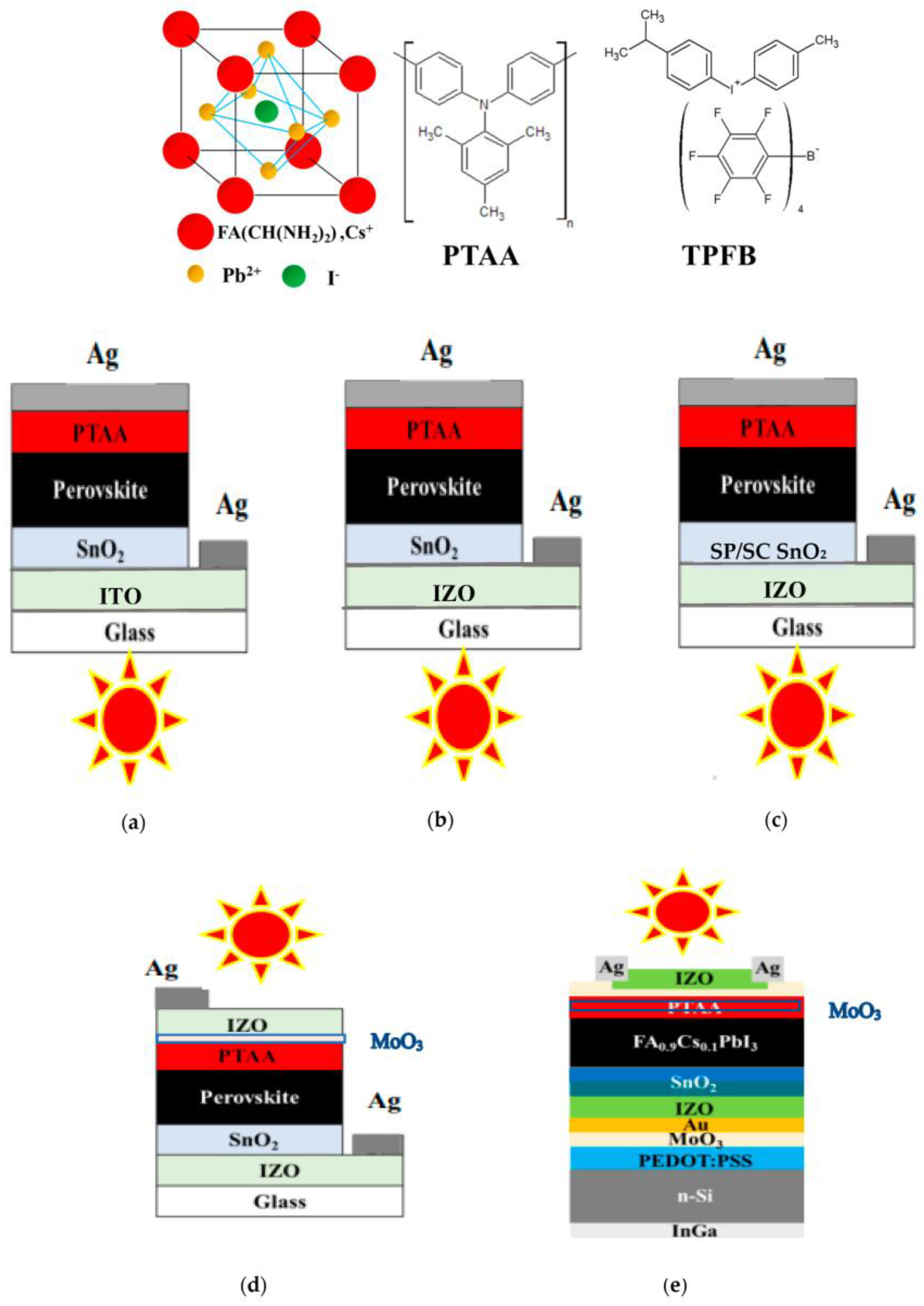
2.1. Structure of PSCs and Monolithic Tandem Solar Cells

Figure 1 shows the schematic diagram of the individual PSCs, i.e., (a) glass/ITO/SnO2/FA0.9Cs0.1PbI3/PTAA(60 wt% TPFB)/Ag, (b) glass/IZO/spin coated (sc) or sputtered (sp) alone SnO2/FA0.9Cs0.1PbI3/PTAA(60 wt.% added TPFB)/Ag, and (c) glass/IZO/two-step sp and sc (sp/sc) SnO2/FA0.9Cs0.1PbI3/PTAA(TPFB)/Ag. The 4-isopropyl-4′-methyldiphenylloidonium tetrakis(pentafluorophenyl)borate (TPFB)-doped poly(bis(4-phenyl)(2,4,6-trimethylphenyl)amine)(PTAA) (Figure 1) was used as HTL because it is thermally more stable than that of 2,2′,7,7′-Tetrakis-5 (N,N-di-4-methoxyphenylamino)-9,9′-spirobifluorene (Spiro-OMeTAD) [27,28,29]. The near-infrared-semitransparent PSCs consisting of (d) glass/IZO/(sp/sc) SnO2/FA0.9Cs0.1PbI3/PTAA(TPFB)/IZO/Ag was also studied with and without MoO3 as a buffer layer between PTAA and IZO. Figure 1e shows the schematic of the monolithic tandem solar cells consisting of a InGa/n-Si/PEDOT:PSS/MoO3/Au NP/IZO/(sp/sc)SnO2/FA0.9Cs0.1PbI3/PTAA(TPFB)/MoO3/IZO/Ag.

2.2. Synthesis Process of Semi-Transparent FACsPbI3 PSCs with PTAA(TPFB) as HTL

For the device (a), an approximately 100 nm thick SnO2 layer was deposited on the commercial ITO (thickness; 100 nm, <17 Ω/sq)/glass substrate as ETL from a 0.15 M SnCl2·2H2O nanoparticle solution. Then, 1.3 M FA0.9Cs0.1PbI3 solution was spin coated at 6000 rpm for 50 s (280–300 nm) using N,N-dimethylformamide (DMF): 1-cyclohexyl-2-pyrrolidone (CHP) (95:5 v/v) as a precursor in a nitrogen atmosphere in a glove box, and then thermally annealed at 170 °C for 10 min to remove residual solvent [30]. Here, 300–350 nm thick FA0.9Cs0.1PbI3 films were synthesized by adjusting the mixing ratio of DMF/CHP using the difference in the vapor pressure and boiling temperature between DMF (153 °C, 4 × 10² Pa) and CHP (286 °C, 7 Pa) with no use of anti-solvent method. In addition, the thiosemicarbazide (TSC) was added to the starting material to enlarge the crystal grain size, resulting in an average grain size of 1–1.5 µm [31]. Then, 60 wt% TPFB-doped PTAA was spin coated as HTL, which has better thermal stability compared to spiro-OMeTAD and can be stored at room temperature. TPFB powder was dissolved in chlorobenzene and a 40 mg/mL solution was added to reduce the resistivity. The effect of adding TPFB in PTAA on the film property and solar cell performance is shown in Figure S1. After that, MoO3 and IZO layers were also deposited as buffer and TCO layers, respectively, using evaporation and sputtering methods.
For devices (b) and (c), approximately 100 nm thick sputtered IZO was deposited on glass at room temperature using a 10.7 wt% ZnO-doped In2O3 target by a sputtering method. The cathode and anode distance were set to 85 mm. The rf power was 0.22 W/cm2 and the flow ratio of O2/Ar was 1/99. Then, the SnO2 layer was formed on IZO by the spin coatings or the sputtering method. However, the IZO is likely to be chemically damaged during the film deposition of the SnO2 layer by spin coat. The formation of SnO2 layer by sputtering also caused plasma damage to the underneath IZO. As a result, the device performance using only spin coating or sputtering of SnO2 was very poor. To overcome this difficulty, a two-step deposition method of the SnO2 layer by sputtering and spin coating (sp/sc) was applied on IZO to avoid the chemical attack of SnCl2·2H2O nanoparticles and the damage from sputtering, followed by thermal annealing at 180 °C for 1 h and UV treatment to promote oxidation. The subsequent film deposition recipe of FA0.9Cs0.1PbI3/PTAA(TPFB)/Ag was the same recipe as in device (a).
To extend the device structure (d) as the top cell in a monolithic tandem device, the near-infrared-transparent PSC IZO/MoO3 bilayer was also formed on PTAA(TPFB) HTL by evaporation and sputtering. The rf power was 0.22 W/cm2, the base pressure was 6 × 10⁻⁴ Pa for 50 min, and the flow ratio was O2/Ar = 90/10. To avoid the sputtering damage during the deposition of IZO on PTAA(TPFB) more efficiently, an approximately 5 nm thick MoO3 was also formed as a buffer layer by evaporation prior to the IZO sputtering. Then, the IZO was sputtered with a mesh ground electrode that was set 20 mm away from the substrate stage to suppress the ion bombardment. As a result, a MoO3/IZO bilayer was formed on PTAA(TPFB)/FA0.9Cs0.1PbI3 without significant plasma damage. Finally, Ag paste (SPI Supplies Silver Paste PlusTM) and InGa paste were used as the top and rear electrodes, respectively.
For the monolithic tandem device (e), first, PEDOT:PSS (CleviosTM PH1000, Heraeus Eprio) with an addition of 7 wt% EG and 0.1% Capstone as surfactant was first used as starting material. The 85–120-nm thick PEDOT:PSS was spin coated on a plane n-Si(100) (ρ: 0.1~0.5 Ω·cm) substrate with a thickness of 250 µm by varying the rotation speed followed by thermally annealed at 140 °C for 30 min to remove residual solvent. Then, a MoO3/IZO bilayer with approximately 5nm thick Au nanoparticles (Au NPs) was formed on the top of PEDOT:PSS as an ICL. The Au NPs were coated by thermal evaporation by adjusting the evaporation speed and the opening diameter of the mechanical shatter. Subsequently, (sp/sc)SnO2/FA0.9Cs0.1PbI3 and PTAA(TPFB) were formed as a photoconductive layer and HTL, respectively. Finally, MoO3/IZO bilayer was formed as a window layer of the top cell and grid Ag top electrode was evaporated. All solution preparations for the perovskite top cell were performed in a nitrogen-purged glove box.

2.3. Structural, Optical, and Electrical Characterizations of FA0.9Cs0.1PbI3 Films

Figure 2 shows the X-ray diffraction (XRD) pattern, UV–visible absorption, and AFM images of approximately 300 nm thick FA0.9Cs0.1PbI3 thin films synthesized with different solution concentrations. The XRD pattern shows that the (100) diffraction peak at 2θ = 14.2° corresponding to a single perovskite α phase is dominant, although the PbI2-related (100) peak appeared at 12.7° for 0.8 and 0.9 M. The UV absorption edge is almost the same except at the wavelength region of 300~600 nm, which may come from the absorption of PbI2 and/or dense film structure dependent on the film thickness. The AFM image also revealed that the average crystal grain size increases with increasing solute concentration of 1~1.5 µm.
Current–voltage (J-V) characteristics in the dark and under AM1.5G 100 mW/cm2 simulated solar light exposure were measured for 1 × 1 cm2 cells using a solar simulator (Bunkoukeiki CEP-25BX), calibrated with a standard silicon cell. The external quantum efficiency (EQE) was measured for the corresponding devices. The dark I-V characteristics of various ICLs between Au and IZO electrodes, i.e., PEDOT:PSS/SnO2, PEDOT:PSS/IZO/SnO2, and PEDOT:PSS/MoO3/Au NP/IZO/SnO2 diodes, were also studied. In addition, the optical constant of PEDOT:PSS, FA0.9Cs0.1PbI3, MoO3/Au NPs/IZO ICL, and PTAA(TPFB)/MoO3/IZO layers was characterized using spectroscopic ellipsometry (SE) (Uvisel plus, HORIBA-Jobin Yvon) over a range of 0.6–5 eV. The n and k spectra of PEDOT:PSS were determined by the spectra fitting procedure using the new amorphous and Drude models considering uniaxial optical anisotropy, i.e., extraordinary and ordinary refractive index and extinction coefficient (nex, kex) and (no, ko) [32,33,34,35].

3. Results and Discussion

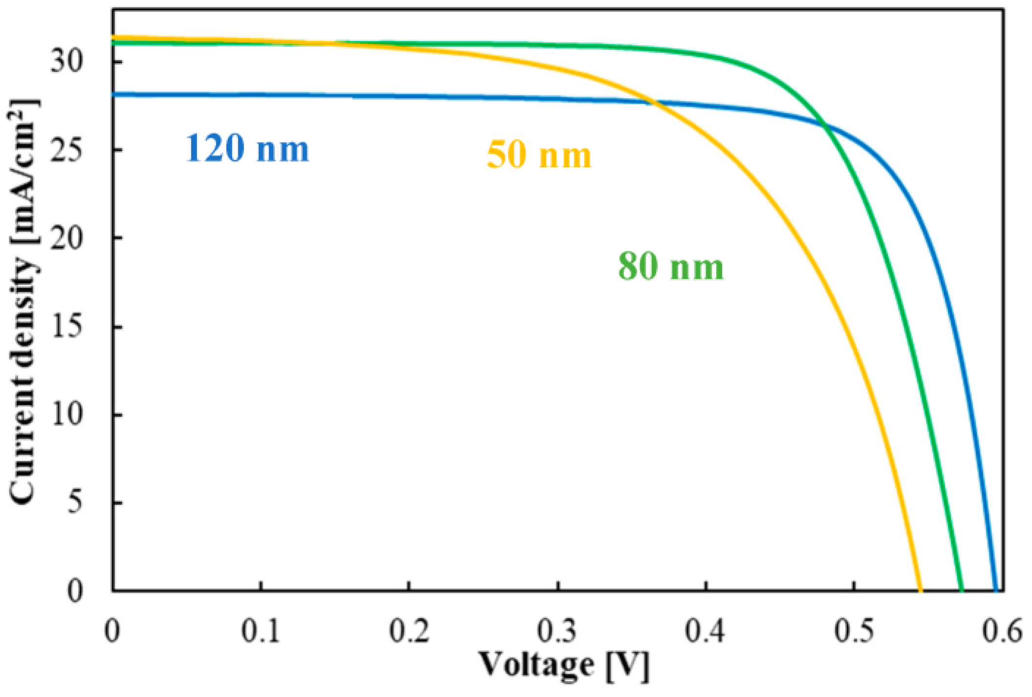
3.1. J-V Characteristics of n-Si/PEDOT:PSS and PSC Solar Cells

Figure 3 shows the J-V characteristics of the individual spin-coated PEDOT:PSS/n-Si solar cells on a planar n-Si substrate with three different layer thicknesses of PEDOT:PSS, i.e., 50, 80, and 120 nm [36,37,38,39]. The performance of the solar cells used in this study is summarized in Table 1. The PCE is 13.0% with a short-circuit current, Jsc, of 31.1 mA/cm2; an open-circuit voltage, Voc, of 0.58 V; and fill factor, FF, of 0.73 when the layer thickness of PEDOT:PSS is set to 80 nm. To understand the potential of the MoO3/IZO-based metal oxide bilayer as an ICL and window layer for n-Si/perovskite tandem solar cells, the planar Si/PEDOT:PSS was used as the bottom cell.
Figure 4 shows the J-V characteristics of individual PSCs consisting of (a) glass/commercialized ITO/(sc)SnO2/FA0.9Cs0.1PbI3/PTAA(TPFB)/Ag, (b) glass/IZO/(sc or sp)SnO2/FA0.9Cs0.1PbI3/PTAA(TPFB)/Ag, glass/IZO/(sp/sc)SnO2/FA0.9Cs0.1PbI3/PTAA (TPFB)/Ag, and (c) near-infrared-transparent glass/IZO/(sp/sc)SnO2/FA0.9Cs0.1PbI3/PTAA(TFPB)/MoO3/IZO/Ag. Here, Ag refers to the top electrode structure provided around the irradiation area of a 5 mm square on the IZO for solar irradiation.
For device (a) with solution process SnO2 as the ETL, the PCE shows a value of 13.5% with a Jsc of 23.3 mA/cm2, a Voc of 0.89 V, and an FF of 0.66. On the other hand, the PV performance deteriorated for the devices for sputtered or solution process SnO2 on IZO. This is due to the chemical attack by the strong acidity of the SnCl2·2H2O nanoparticle solution and the damage to the underneath IZO by sputtering. To overcome this problem, (b) the two-step deposition method of SnO2 by both sputtering and spin coating on IZO was applied. As a result, the sheet resistance of the SnO2 decreased from 680 to 11 Ω·cm2 and the PCE increased to 13.3% with a Jsc of 23.3 mA/cm2, Voc of 0.89 V, and FF of 0.66. Thus, the sputtered IZO layer at room temperature acts as the bottom transparent electrode by using the two-step SnO2 ETL layer.
Figure 4c shows the J-V characteristics of the near-infrared-semitransparent IZO/(sp/sc)SnO2/FA0.9Cs0.1PbI3/PTAA(TPFB)/IZO/Ag devices without and with a MoO3 layer between the PTAA(TPFB) and top IZO for extending to monolithic tandem solar cells as a top cell. The series resistance of PTAA(TPFB)/IZO is 680 Ω·cm2 and the PV performance was very poor when no MoO3 device was inserted, whereas the PCE improved to 9.02% with a Jsc of 14.8 mA/cm2, a Voc of 0.87 V, and an FF of 0.61 when a 5 nm thick p-type MoO3 was inserted as a buffer layer. These results are based on the suppression of sputtering damage for the PTAA(TPFB) HTL, which preserves the smooth band alignment. These results suggest that the PTAA (60 wt% mixed TPFB) and MoO3/IZO function as a HTL and window layer, respectively, for near-infrared-semitransparent FA0.9Cs0.1PbI3 PSCs. Table 2 summarizes the solar cell parameters for the corresponding (a)–(c) devices. These results suggest that the MoO3/IZO bilayer acts as a window layer for the near-infrared-semitransparent PSCs.

3.2. J-V Characteristics of n-Si/FA0.9Cs0.1PbI3 PSC Monolithic Tandem Solar Cells with n-Si/PEDOT:PSS Device as a Bottom Cell

Figure 5a shows the J-V characteristics of the monolithic tandem solar cells consisting of Ag/IZO/MoO3/FA0.9Cs0.1PbI3/SnO2/Au NPs/IZO/MoO3/PEDOT:PSS/n-Si/InGa with different layer thicknesses of the IZO at the ICL. To meet the requirements of an ICL, the following items must be met. The charge recombination depends on the alignment of the Fermi level of the HTL and ETL. It is required that (1) the ICL should have a high optical transmittance to minimize optical losses; (2) between the ETL and HTL, a quasi-ohmic contact should be made to allow for electron–hole charge extraction and recombination; (3) the ICL should be robust enough to protect the underlying active layer from dissolution by the processing solvents for the top cell; and (4) the ICL should be chemically stable to enhance the stability and lifetime of the tandem device.
The J-V characteristics of the corresponding tandem cells are also shown with different thicknesses of MoO3, 5 and 10 nm, as a buffer layer at the ICL. The Voc increases with an increased layer thickness of IZO, although the FF is still poor. In Figure 5b, the I-V curves are also shown in the corresponding tandem device using MoO3 and Au NPs at the IZO/MoO3 interface. Both the FF and Voc were improved significantly by introducing Au NPs at the IZO/MoO3 interface, suggesting that the charge extraction and recombination are enhanced.
Figure 6 shows the J-V characteristics of the monolithic tandem solar cells consisting of Ag/IZO/MoO3/FA0.9Cs0.1PbI3/SnO2/IZO(46 nm)/Au NP/MoO3/PEDOT:PSS/n-Si/Ag with different layer thicknesses of IZO, 40, 80, and 100 nm, as a window layer. The J-V characteristics were improved by adjusting the IZO layer thickness for a window layer of 60–80 nm, which was 1.5 times thicker than that of the ICL. These findings suggest that the MoO3/IZO bilayer without and with Au NPs acts as a window layer and ICL, respectively, by adjusting each layer’s thickness. However, the EQE for the corresponding solar cell devices revealed that the contributions to the power generation of the top PSC are dominant and the bottom PEDOT:PSS/n-Si cell is much smaller due to the insufficient optimization the of the bottom PEDOT:PSS device.
Figure 7a shows the J-V characteristics of the n-Si/PSC monolithic tandem solar cells consisting of InGa/n-Si/PEDOT:PSS/MoO3/Au NPs/IZO/(sp/sc)SnO2/FA0.9Cs0.1PbI3/PTAA(TPFB)/MoO3/IZO/Ag with a different layer thickness of PEDOT:PSS (Figure 1e). The inset shows a cross-sectional SEM image of the corresponding monolithic tandem cell. The layer thickness was almost consistent with those of the SE spectra analysis (Figures S3 and S4). Table 3 summarizes the solar cell parameter for the corresponding devices. As a result, the PCE exhibits a value of 19.3% with a Jsc of 17.8 mA/cm2, Voc of 1.48 V, and FF of 0.73 for the reverse scan when the layer thickness of the MoO3 (5 nm), Au NPs (approximately 10 nm), IZO (42 nm for ICL and 68 nm for window layer), PEDOT:PSS (80 nm), and FA0.9Cs0.1PbI3 (360 nm) are adjusted. The Voc of 1.48 V corresponds to the sum of 0.59 V of the bottom n-Si/PEDOT:PSS cell and 0.89 V of the top PSC corresponding device (d). The EQE also revealed that both the top and bottom cells contribute to the power generation equivalently (Figure 7b). These results indicate that the MoO3/IZO bilayer with Au NPs effectively aligns the energy levels in the ICL and improves the charge extraction and charge recombination. The EQE originates from the top PSC and bottom n-Si/PEDOT:PSS cells, although the value is still lower due to insufficient optimization of the top and bottom cells. The EQE for the monolithic device with an 80 nm thick PEDOT:PSS revealed that both the top and bottom cells contribute to the power generation equivalently (Figure 7b). These results indicate that the MoO3/IZO bilayer with Au NPs effectively aligns the energy levels in the ICL and improves the charge extraction and charge recombination. The EQE originates from the top PSC and bottom n-Si/PEDOT:PSS cells, although the value is still lower due to the insufficient optimization of the top and bottom cells.

3.3. Optical and Electrical Characterizations of MoO3/IZO-Based Bilayer as Window Layer and IC for FA0.9Cs0.1PbI3/n-Si Monolithic Tandem Solar Cells

Figure 8 shows the normal optical transmittance, T, spectra for the corresponding MoO3/IZO bilayer without and with Au NPs. The optical transmittance of the MoO3/IZO bilayer is almost constant at 75–80% except for the UV region due to the optical absorption of IZO. On the other hand, the optical transmittance of the MoO3/IZO bilayer with Au NPs shows a dimple at 600–700 nm due to the plasmonic optical absorption of the Au NPs. The average size and number density of the Au NPs cause the optical loss. Thus, the precise control of the size distribution and the number density of the Au NPs are required to suppress the optical loss as well as to promote the charge extraction at the IZO/MoO3 interface for further increasing the performance of the FA0.9Cs0.1PbO3/n-Si monolithic tandem solar cell.
Figure 9a shows the sheet resistance of the sputter-deposited IZO on glass at room temperature plotted as a function of the film thickness. The sheet resistance decreased with increased film thickness and it tends to saturate at 40~80 Ω·sq when the layer thickness is above 40 nm. Figure 9b shows the dark J-V characteristics of various ICLs, PEDOT:PSS/SnO2, PEDOT:PSS/IZO/SnO2, and PEDOT:PSS/MoO3/Au NP/IZO/SnO2 used for the corresponding n-Si/perovskite monolithic tandem solar cells. All the J-V curves show a quasi-ohmic contact. The series resistance at 1.5 V decreased from 6.8 to 6.2 Ω·cm2 by inserting IZO and further to 4.6 Ω·cm2 by inserting an approximately 5 nm thick Au NP layer between the MoO3 and IZO layer. The sheet resistance of the IZO film also decreased to 141 Ω/sq when the film thickness was above 40–50 nm. As a result, the optical transmittance of the IZO (46 nm)/Au NP (~10 nm)/MoO3 (5 nm) remains at 75–80% in the entire wavelength range of 400–1200 nm; although, the n value of the MoO3 and IZO was 1.7–1.9, which helps to suppress the optical loss of the transmitted sunlight through the top PSCs.
Figure 10 shows the schematic energy level diagrams of the ICL of the MoO3/Au NPs/IZO. The valence band offset between the highest occupied molecular orbital (HOMO) energy top of PEDOT:PSS, p-type MoO3, and the valence band top of n-Si is less than ~0.3 eV, suggesting that the hole current flows to the emitter without any significant energy barriers. In contrast, the IZO/Au junction will have a Schottky junction due to the large work function of the Au metal at the n-type IZO, which would result in the resistance and suppression of the carrier recombination. The fill factor is not completely reduced in the ICL. In particular, for the MoO3 layer, the performance strongly depends on the oxygen vacancies. Energy level alignment can be achieved in MoO3/Au by Fermi level pinning. It is well-known that the gap states caused by oxygen vacancies in the transition metal oxide act as dopants that promote electron–hole pair recombination and ICL conductivity. In the case of IZO, it is reported that the Fermi level (FB) in transparent conductive oxide (TCO) such as InGaO (IGO) and IZO is very sensitive to the oxygen flow ratio of O2/Ar and FB exists within the conduction band when an O2/Ar ratio is up to ~1% in Ar [40,41]. In general, the correlation between the bandgap and carrier concentration in inorganic TCO can be explained by the Burstein–Moss effect [42,43,44,45]. It has been also applied as an ICL for the perovskite–perovskite tandem solar cells [46,47]. These results suggest that the MoO3/Au NPs/IZO tri-layer and MoO3/IZO bilayer act as the ICL and window layer, respectively, for n-Si/perovskite tandem solar cells.

3.4. Optical Simulation Study of the n-Si/FA0.9Cs0.1PbI3 PSC Monolithic Tandem Solar Cells by SE

Figure 11a shows the measured (Ψ, Δ) spectra at an incident angle of 70° of the IZO/MoO3/PTAA(TPFB)/FA0.9Cs0.1PbI3/SnO2/IZO/Au NP/MoO3/PEDOT:PSS/n-Si monolithic tandem structure. The fitting procedure was performed using a new amorphous model [48] combined with the Drude model for free carrier absorption and IZO [49], and the reference Au NP spectrum [50] by considering the interface mixing layer of the IZO and Au NPs with a volume fraction of Au NPs and IZO, fAuNP, and fIZO, and layer thickness as variables. Figure 11b shows the best-fit normal incident T and R spectra of the top IZO/MoO3/PTAA(TPFB)/FA0.9Cs0.1PbI3/SnO2 cell determined by the fitting procedure of the <n> and <k> spectra using the reference spectra of PTAA(TPFB), (sc/sp)SnO2, and FA0.9Cs0.1PbI3 (Figure S3). The best-fit optical model is also shown on the right. The increase in the T at longer than the 550 nm corresponds to that from the top near-infrared-semitransparent PSCs transmitted to the bottom PEDOT:PSS/n-Si cell. However, there still remained surface reflectance R of 20–30% in the entire wavelength region.
In Figure 11c, the R spectra from the bottom IZO/MoO3/PEDOT:PSS/n-Si/Ag cell are shown without and with Au NPs at the MoO3/IZO interface. The best-fit optical structure was obtained by considering the intermixing layer of Au NP and IZO with volume fraction ratio of fAuNP/fIZO = 30:70 and an approximately 5~7 nm thickness. The best-fit n and k spectra of the MoO3 and IZO are shown in Figure S3 including the reference Au NP. For metallic spheres with Drude dielectric function, the Maxwell Garnett theory (MG) [51,52] describes a Lorentzian with a resonance frequency  ω 0 ,
ω 0 2 = ω p 2 ( 1 F ) ε + 2 ε a
where  ω p  is plasma frequency,  ε a  is the dielectric constant of the Au particle,  ε  is the infinite dielectric constant, and F is the volume fraction of the Au NP embedded in the IZO. As the fAuNP is increased, the MGT predicts a red shift of the resonance frequency. According to the resonance frequency shift, the average size of the spherical Au NPs used in this study corresponds to approximately 5~10 nm, which is almost consistent with that of the TEM image (Figure 11c).
The R from the bottom cell with Au NPs was decreased at the 350–800 nm range and longer than 950 nm region, which caused the optical loss. However, the reduction of the R was suppressed to be10–15% in the entire wavelength region by adjusting the size and number density of Au NPs. To further suppress and avoid these optical loss, highly conductive monolayer sheet is required candidate such as graphene.
In Figure 11d, the R spectra are also shown for the Ag/IZO/MoO3/PTAA(TPFB)/FA0.9Cs0.1PbI3/SnO2/IZO/Au NP/MoO3/PEDOT:PSS/n-Si/Ag including those with a TiO2 or SiO2 layer alone and a TiO2/SiO2 layer with a compositional gradient toward the film thickness of a 200 nm as an AR coat layer. The R is suppressed to be less than 0.1 in the 300~980 nm range, which will improve the solar cell performance. As a result, the best performance can be expected for a layer thickness of the IZO as the window layer and ICL of approximately 60–70 and 50 nm, respectively.

4. Conclusions

The MoO3/IZO bilayer with and without Au NPs acts as an ICL and window layer, respectively, for (n-Si/PEDOT:PSS)/FA0.9Cs0.1PbI3 perovskite monolithic tandem solar cells. The MoO3/IZO bilayer with Au NPs can align the energy levels between MoO3 and IZO, which play a significant role in the charge extraction and recombination within the ICL. The MoO3/IZO bilayer also acts as a window layer of the top perovskite cell. A PCE of 19.3% was achieved in the reverse scan mode with a Jsc of 17.8 mA/cm2, Voc of 1.48 V, and FF of 0.73 by adjusting a layer thickness of the MoO3 (5 nm), Au NPs (approximately 10 nm), IZO (42 nm for ICL and 80 nm for window layer), PEDOT:PSS (80 nm), and FA0.9Cs0.1PbI3 (360 nm).

Supplementary Materials

The following supporting information can be downloaded at https://www.mdpi.com/article/10.3390/cryst14010068/s1, Figure S1: (a) Molecular structure of PTAA and TPFB. (b) Conductivity of PTAA as a function of TPFB mixing concentration. -M, -U. and -UH present molecular weight, M: 1.1 kDa, H: 90 kDa, and UH: 325 kDa in PTAA. (c) Stability test of I-V curve of single PSCs with spiro-OMeTAD and PTAA(TPFB) as HTL for 85 °C and 85%. Figure S2: XRD pattern of FA0.9Cs0.1PbI3 thin films on spin coated and sputtered SnO2 substrates. Figure S3: The n and k spectra of MoO3, IZO, Au NPs components for the IZO/MoO3 bilayer with and without Au NPs determined by the spectra fitting procedure. Figure S4: The n and k spectra of 60 wt% TPFB mixed PTAA, FA0.9Cs0.1PbI3, and SnO2 determined by the spectra fitting procedure. Refs. [48,49,50] are cited.

Author Contributions

Methodology, H.S.; validation, Y.W. and Y.I.; formal analysis, R.U.; investigation, R.U.; data curation, R.U.; writing—original draft preparation, H.S.; visualization, H.S.; project administration, H.S.; funding acquisition, H.S. All authors have read and agreed to the published version of the manuscript.

Funding

This study is in part supported by KAKENHI Grant number 20K05318.

Data Availability Statement

The authors declare that the data supporting the findings of this study are available within the paper and its supplementary information files.

Acknowledgments

The authors appreciate Ryo Ishikawa of Saitama University for supporting experimental and fruitful discussion. The authors also appreciate T. Kurosu and T. Hanajiri of Bio-Nanoelectronics Center of Toyo University for supporting the SEM observation.

Conflicts of Interest

Authors Yoko Wasai and Yuki Izumi were employed by the company Horiba Techno Service, Ltd. Two the authors also declare that the research was conducted in the absence of any commercial or financial relationships that could be construed as a potential conflict of interest.

References

  1. National Renewable Energy Laboratory (NREL). Best Research-Cell Efficiency Chart. 2023. Available online: https://www.nrel.gov/pv/cell-efficiency.html (accessed on 27 December 2023).
  2. Shockley, W.; Queisser, H. Detail balance limit of efficiency of p-n junction solar cells. J. Appl. Phys. 1961, 32, 510–519. [Google Scholar] [CrossRef]
  3. Ruhle, S. Tabulated values of the Schockley-Queisser limit for single junction solar cells. Sol. Energy 2016, 130, 139–147. [Google Scholar] [CrossRef]
  4. Akhil, S.; Akash, S.; Pasha, A.; Kulkarni, B.; Jalalah, M.; Alsaiari, M.; Harraz, F.A.; Balakrishna, R. Review on perovskite silicon tandem solar cells: Status and prospects, 2T, 3T, and 4T for real worlds conditions. Mater. Des. 2021, 211, 110138. [Google Scholar] [CrossRef]
  5. Maioa, J.; Ballie, C.; Johin, E.; Hoke, E.; Akey, A.; Nguyen, W.; McGehee, M.; Bounassisi, T. A 2-termnal perovskite/silicon multijunction solar cell enabled by a silicon tunnel junction. Appl. Phys. Lett. 2005, 106, 121105. [Google Scholar] [CrossRef]
  6. Lamanna, E.; Matteocci, F.; Calabro, E.; Serenelli, L.; Salza, E.; Martini, L.; Menchini, F.; Izzi, M.; Agresti, A.; Pescetelli, S.; et al. Mechanically Stacked, Two-terminal graphene-based perovskite/silicon tandem solar cell with efficiency over 26%. Joule 2020, 15, 865–881. [Google Scholar] [CrossRef]
  7. Goldshmidt, J.; Do, C.; Peters, M.; Goetzberger, A. Spectral splitting module geometry that utilizes light trapping. Sol. Energy Mater. Sol. Cells 2013, 108, 57–64. [Google Scholar] [CrossRef]
  8. Uzu, H.; Ichikawa, M.; Hino, M.; Nakano, K.; Meguro, T.; Hernándes, J.; Kim, H.-S.; Park, N.-G.; Yamamoto, K. High efficiency solar cells combining a perovskite and a silicon heterojunction solar cells via an optical splitting system. Appl. Phys. Lett. 2015, 106, 013506. [Google Scholar] [CrossRef]
  9. Zhu, S.; Guo, X.; Ren, Y.; Zhang, C.; Li, S.; Tong, Y.; Shi, B.; Guo, S.; Fan, L.; Ren, H.; et al. Transparent electrode for monolithic perovskite/silicon-heterojunction two-terminal tandem solar cells. Nano Energy 2018, 45, 280–286. [Google Scholar] [CrossRef]
  10. Sheng, R.; Ho-Baillie, A.; Huang, S.; Keevers, M.; Hao, X.; Jiang, L.; Cheng, Y.; Green, M. Four-terminal tandem solar cells using CH3NH3PbBr3 by spectrum splitting. J. Phys. Chem. Lett. 2015, 6, 3931–3934. [Google Scholar] [CrossRef]
  11. Werner, J.; Barraud, L.; Walter, A.; Bräuninger, M.; Sahli, F.; Sacchetto, D.; Tetreault, N.; Paviet-Salomon, B.; Moon, S.-J.; Allebé, C.; et al. Efficient near-infrared-transparent perovskite solar cells enabling direct comparison of 4-terminal and monolithic perovskite/silicon tandem cells. ACS Energy Lett. 2015, 1, 474–480. [Google Scholar] [CrossRef]
  12. Yin, X.; Song, Z.; Li, Z.; Tang, W. Toward ideal hole transport materials: A review on recent progress in dopant-free hole transport materials for fabricating efficinet and stable perovskite solar cells. Energy Environ. Sci. 2020, 13, 4057–4086. [Google Scholar] [CrossRef]
  13. A-Ashouri, A.; Köhnen, E.; Li, B.; Magomedov, A.; Hempel, H.; Caprioglio, P.; Márquez, J.; Grischek, M.; Kegelmann, L.; Skroblin, D.; et al. Monolithic perovskite/silcion tandem solar cells with >29% efficiency by enahanced hole extraction. Science 2020, 370, 1300–1309. [Google Scholar] [CrossRef] [PubMed]
  14. Qing, J.; Zhong, Z.-F.; Li, Y.; Li, B.-J.; Zhou, X. MoO3/Ag/Al/ZnO intermediate layer for inverted tandem polymer solar cells. Chin. Phys. B 2014, 23, 038802. [Google Scholar] [CrossRef]
  15. Lu, S.; Guan, X.; Li, X.; Sha, W.; Xie, F.; Liu, H.; Wang, J.; Huang, F.; Choy, W. A new interconnecting layer of metal oxide/dipole layer/metal oxide for efficient tandem organic solar cells. Adv. Energy Mater. 2015, 5, 1500631. [Google Scholar] [CrossRef]
  16. Yusoff, A.; Kim, D.; Kim, H.; Shneider, F.; Silva, W.; Jang, J. A high efficiency solution processed polymer inverted triple-junction solar cell exhibiting a power conversion efficiency of 11.83%. Energy Environ. Sci. 2015, 8, 303–316. [Google Scholar] [CrossRef]
  17. Greiner, M.; Chai, L.; Helander, M.; Tang, W.-M.; Lu, Z.-H. Metal/Metal-oxide interfaces: How metal contacts affect the work function and band structure of MoO3. Adv. Func. Mater. 2013, 23, 215–226. [Google Scholar] [CrossRef]
  18. Grant, T.; Gorisse, T.; Dautel, O.; Wantz, G.; Lessard, B. Multifunctional ternary additive in bulk heterojunction OPV: Increased device performance and stability. J. Mater. Chem. A 2017, 5, 1581–1587. [Google Scholar] [CrossRef]
  19. Popov, A.; Brasiunas, B.; Damaskaite, A.; Plikusiene, L.; Ramanavicis, A.; Ramannavicine, A. Electrodeposited gold nanostructures for the enhancement of electrochromic properties of PANI–PEDOT film deposited on transparent electrode. Polymers 2020, 12, 2778. [Google Scholar] [CrossRef]
  20. Liu, Q.; Ono, M.; Tang, Z.; Ishikawa, R.; Shirai, H. Highly efficient crystalline silicon/Zonyl fluorosurfactant-treated organic heterojunction solar cells. Appl. Phys. Lett. 2012, 100, 183901. [Google Scholar] [CrossRef]
  21. Xia, Y.; Sun, K.; Quyang, J. Highly conductive poly(3,4-ethylene dioxythiophene):poly(styrene sulfonate) films treated with an amphiphilic fluoro compound as the transparent electrode of polymer solar cells. Energy Environ. Sci. 2012, 5, 5325–5332. [Google Scholar] [CrossRef]
  22. Zielke, D.; Pazidis, A.; Werner, F.; Schmidt, J. Organic-silicon heterojunction solar cells on n-type silicon wafers: The backPEDOT concept. Sol. Energy Mater. Sol. Cells 2014, 131, 110–116. [Google Scholar] [CrossRef]
  23. Wu, S.; Aghdassi, N.; Song, T.; Duhm, S.; Lee, S.-T.; Sun, S. Nanostructured Si/Organic heterojunction solar cells with high open-circuit voltage via improving junction quality. Adv. Func. Mater. 2016, 26, 5035–5041. [Google Scholar] [CrossRef]
  24. Liu, Y.; Zhang, J.; Wu, H.; Cui, W.; Wang, R.; Ding, K.; Lee, S.-T. Low-temperature synthesis of TiOx passivation layer for organic-silicon heterojunction solar cell with a high-open-circuit voltage. Nano Energy 2017, 34, 257–2643. [Google Scholar] [CrossRef]
  25. Kasahara, K.; Hossain, J.; Harada, D.; Ichikawa, K.; Ishikawa, R.; Shirai, H. Crystalline-Si heterojunction with organic thin-layer (HOT) solar cell module using poly(3,4-ethylenedioxythiophene):poly(styrene sulfonate) (PEDOT:PSS). Sol. Energy Mater. Sol. Cells 2017, 181, 60–70. [Google Scholar] [CrossRef]
  26. Zielke, D.; Gogolin, R.; Halbich, M.-U.; Marquardt, C.; Lövenich, W.; Sauer, R.; Schmidt, J. Large-area PEDOT:PSS/c-Si heterojunction solar cells with screen-printed metal contacts. Sol. RPL 2018, 2, 1700191. [Google Scholar] [CrossRef]
  27. Yang, W.S.; Park, B.W.; Jung, E.H.; Jeon, N.J.; Kim, Y.C.; Lee, D.U.; Shin, S.S.; Seo, J.; Kim, E.K.; Noh, J.H.; et al. Iodide management in formamidinium-lead-halide–based perovskite layers for efficient solar cells. Science 2017, 3560, 1376–1379. [Google Scholar] [CrossRef] [PubMed]
  28. Lee, I.; Rolston, N.; Brunner, P.L.; Dauskardt, R.H. Hole transport layer molecular weight and doping effects on perovskite solar cell efficiency and mechanical behavior. ACS Appl. Mater. Interfaces 2019, 11, 23757–23764. [Google Scholar] [CrossRef]
  29. Ko, Y.; Kim, Y.; Lee, C.; Kim, Y.; Jun, Y. Investigation of hole-transporting Poly(triarylamine) on aggregation and charge transport for hysteresisless scalable planar perovskite solar cells. ACS Appl. Mater. Interfaces 2018, 10, 11633. [Google Scholar] [CrossRef]
  30. Ishikawa, R.; Ueno, K.; Shirai, H. Fabrication of FA0.8Cs0.2PbI3 perovskite thin films by one-step method using 1-Cyclohexyl-2-pyrrolidone as additive with application to n-i-p planar-structured solar cells. Chem. Lett. 2018, 47, 905–908. [Google Scholar] [CrossRef]
  31. Kawamura, K.; Ishikawa, R.; Wasai, Y.; N-Gabain, N.; Kurosu, S.; Ukai, T.; Tokuda, M.; Fujii, Y.; Hanajiri, T.; Ueno, K.; et al. Role of the solvent in large grain growth of inorganic-organic halide FA0.8Cs0.2PbIxBr3−x perovskite thin-films monitored by ellipsometry. J. Vac. Sci. Technol. B 2019, 37, 062401. [Google Scholar] [CrossRef]
  32. Forouhi, R.; Bloomer, I. Optical dispersion relations for amorphous semiconductors and amorphous dielectrics. Phys. Rev. B 1986, 34, 7018–7026. [Google Scholar] [CrossRef] [PubMed]
  33. Forouhi, A.R.; Bloomer, I. Optical properties of crystalline semiconductors and dielectrics. Phys. Rev. B 1988, 38, 1865. [Google Scholar] [CrossRef] [PubMed]
  34. Jellison, G.E.; Modine, F.A. Optical functions of silicon between 1.7 and 4.7 eV at elevated temperatures. Phys. Rev. B 1996, 69, 371–374. [Google Scholar] [CrossRef]
  35. Pettersson, L.A.A.; Carlsson, F.; Inganäs, O.; Arwin, H. Spectroscopic ellipsometry studies of the optical properties of doped poly(3,4-ethylnedioxthiophene): An anisotropic metal. Thin Solid Films 1998, 313–314, 356–361. [Google Scholar] [CrossRef]
  36. Funada, S.; Ohki, T.; Liu, Q.; Ishimaru, Y.; Ueno, K.; Shirai, H. Correlation between the fine structure of spin-coated PEDOT:PSS and the photovoltaic performance of organic/crystalline-silicon heterojunction solar cells. J. Appl. Phys. 2016, 120, 033103. [Google Scholar] [CrossRef]
  37. Shirai, H.; Liu, Q.; Ohki, T.; Ishikawa, R.; Ueno, K. Optical anisotropy and compositional ratio of conductive polymer PEDOT:PSS and their effect on photovoltaic performance of crystalline silicon/organic heterojunction solar cells. In Advances in Silicon Solar Cells; Springer: Berlin/Heidelberg, Germany, 2018; pp. 137–159. [Google Scholar] [CrossRef]
  38. Islam, A.T.M.; Ishikawa, R.; Shirai, H.S. Solution-Processed Crystalline Silicon Heterojunction Solar Cells. In Advanced Nanomaterials for Solar Cells and Light Emitting Diodes; Elsevier: Amsterdam, The Netherlands, 2019; Chapter 4; pp. 137–159. [Google Scholar] [CrossRef]
  39. Liu, Q.; Imamura, T.; Hiate, T.; Khatri, I.; Tang, Z.; Ishikawa, R.; Ueno, K.; Shirai, H. Optical anisotropy in solvent-modified poly(3,4-ethylndioxythiphene):poly(styrenesulfonic acid) and Its effect on the photovoltaic performance of crystallin silicon/organic heterojunction solar cells. Appl. Phys. Lett. 2013, 102, 243902. [Google Scholar] [CrossRef]
  40. Electronic State Analysis of IZO (In-Zn-O) Film by XPS/REELS Analysis. Available online: https://cs2.toray.co.jp/news/trc/news_rd01.nsf/0/9C01B563EA4EBC81492586690029A6BA?open (accessed on 27 December 2023).
  41. Shigesato, Y.; Takaki, S.; Haranou, H. Crystallinity and electrical properties of tin-doped indium oxide films deposited by DC magnetron sputtering. Appl. Surf. Sci. 1991, 48/49, 269–275. [Google Scholar] [CrossRef]
  42. Woollam, J.A.; McGahan, W.A.; Johs, B. Spectroscopic ellipsometry studies of indium tin oxide and their flat panel display materials. Thin Solid Films 1994, 241, 44–46. [Google Scholar] [CrossRef]
  43. Hamberg, I.; Granqvist, C. Evaporated Sn-doped In2O3 films: Basic optical properties and applications to energy-efficient windows. J. Appl. Phys. 1986, 60, R123–R159. [Google Scholar] [CrossRef]
  44. Jin, Z.-C.; Hamberg, I.; Granqvist, C.G. Optical properties of sputter-deposited ZnO:Al thin films. J. Appl. Phys. 1988, 64, 5117. [Google Scholar] [CrossRef]
  45. Fujiwara, H.; Kondo, M. Effects of carrier concentration on the dielectric Function of ZnO:Ga and In2O3:Sn studied by spectroscopic ellipsometry: Analysis of free-carrier and band-edge absorption. Phys. Rev. B 2005, 71, 075109. [Google Scholar] [CrossRef]
  46. Yang, Y.; Kang, D.-W.; Kim, Y.-S. An Efficient and thermally stable interconnecting layer for tandem organic solar cells. Sol. Energy 2017, 155, 552–560. [Google Scholar] [CrossRef]
  47. Ho, C.H.Y.; Kothari, J.; Fu, X.; So, F. Interconnecting layers for tandem organic solar cells. Mater. Today Energy 2021, 21, 100707. [Google Scholar] [CrossRef]
  48. Available online: https://static.horiba.com/fileadmin/Horiba/Company/About_HORIBA/Readout/JA/R56J/R55J_07.pdf (accessed on 27 December 2023).
  49. Chiang, Y.-H.; Peng, C.-C.; Chen, Y.-H.; Tung, Y.-L.; Tsai, S.-Y.; Chen, P. The utilization of IZO transparent conductive oxide for tandem and substrate type perovskite solar cells. J. Phys. D Appl. Phys. 2018, 23, 424002. [Google Scholar] [CrossRef]
  50. Nakamura, T.; Moriyama, T.; Gabin, N.N.; Adachi, S. Emission decay rate of a light emitter on thin metal films. Jpn. J. Appl. Phys. 2014, 53, 045201. [Google Scholar] [CrossRef]
  51. Maxwell-Garnett, J. XII. Colours in metal glasses and metallic films. Phil. Trans. R. Soc. Lond. 1904, 203, 385–420. [Google Scholar]
  52. Matrton, J.P.; Lemon, J.R. Optical Properties of aggregated metal systems. I. Theory. Phys. Rev. B 1971, 4, 271. [Google Scholar] [CrossRef]
Figure 1. Schematic diagram of the device structures of individual PSCs (a) glass/commercialized ITO/(sc)SnO2/FA0.9Cs0.1PbI3/PTAA(TPFB)/Ag, (b) glass/IZO/(sc)SnO2/FA0.9Cs0.1PbI3/PTAA(TPFB)/Ag, (c) glass/IZO/(sc or sp)SnO2/FA0.9Cs0.1PbI3/PTAA(TPFB)/Ag, (d) near-infrared-transparent PSC device consisting of glass/IZO/(sp/sc)SnO2/FA0.9Cs0.1PbI3/PTAA/MoO3/IZO/Ag, and (e) n-Si/PEDOT:PSS/MoO3/Au NP/IZO/(sp/sc) SnO2/FA0.9Cs0.1PbI3/PTAA(TPFB)/MoO3/IZO/Ag monolithic tandem devices.
Crystals 14 00068 g001
Figure 2. (a) XRD pattern, UV absorbance, and AFM image of SC FA0.9Cs0.1PbI3 films on glass synthesized at different solution concentrations, 0.7, 0.8, and 0.9M. (b) Effect of solution concentration on the surface morohology.
Crystals 14 00068 g002
Figure 3. J-V characteristics of spin-coated n-Si/PEDOT:PSS devices with three different layer thicknesses of PEDOT:PSS, 50, 80, and 120 nm used in this study.
Crystals 14 00068 g003
Figure 4. (a) J-V characteristics of individual spin coat SnO2/FA0.9Cs0.1PbI3/PTAA(TPFB)/Ag cells with (a) commercial ITO and sputtered (sp) IZO as TCO electrode. (b) J-V characteristics of a single IZO/(sp/sc) SnO2/FA0.9Cs0.1PbI3/PTAA(TPFB)/Ag device with two-step sp/sc SnO2. (c) J-V curves of near-infrared-semitransparent IZO/(sp/sc) SnO2/FA0.9Cs0.1PbI3/PTAA(TPFB)/IZO devices with and without ~5 nm thick MoO3 as a buffer layer.
Crystals 14 00068 g004
Figure 5. (a) J-V characteristics of the monolithic tandem solar cells consisting of Ag/IZO/MoO3/FA0.9Cs0.1PbI3/SnO2/Au NPsIZO/PEDOT:PSS/n-Si/InGa with different layer thicknesses of IZO, 5 (black), 20 (orange), and 50 nm (blue) for the ICL. Solid and dashed lines correspond to reverse and forward scans, respectively. (b) J-V characteristics of the corresponding tandem solar cells in the forward and reverse scans with and without Au NPs at the MoO3/IZO interface.
Crystals 14 00068 g005
Figure 6. (a) J-V characteristics of the monolithic tandem solar cells consisting of Ag/IZO/MoO3/FA0.9Cs0.1PbI3/SnO2/Au NPs/IZO (46 nm)/PEDOT:PSS/n-Si/Ag with different layer thicknesses of IZO as a window layer, 40, 80, and 100 nm. (b) EQE for the 110/46 nm n-Si/FA0.9Cs0.1PbI3 PSC tandem solar cell device.
Crystals 14 00068 g006
Figure 7. (a) J-V characteristics of monolithic tandem solar cells consisting of InGa/n-Si/PEDOT:PSS/MoO3/Au NPs/IZO/(sp/sc)SnO2/FA0.9Cs0.1PbI3/PTAA(TPFB)/MoO3/IZO/Ag with three different layer thicknesses, 50, 80, and 120 nm, of PEDOT:PSS. (b) EQE and 1-R for the tandem device with an 80 nm thick PEDOT:PSS/n-Si device as the bottom cell. EQE for FA0.9Cs0.1PbI3 top cell (red), for bottom Si/PEDOT:PSS cell (peppermint green), total EQE (yellow),and 1-R (light green).
Crystals 14 00068 g007
Figure 8. Optical transmittance spectra of the 5 nm thick Au NPs inserted into the IZO/MoO3 bilayer obtained by the standard UV–visible transmittance (dotted line). Optical transmittance spectra obtained from the SE for the MoO3/IZO bilayer with (yellow line) and without (green line) inserting Au NPs layer.
Crystals 14 00068 g008
Figure 9. (a) Sheet resistance of sputter IZO deposited on glass at room temperature as a function of film thickness. (b) Dark J-V characteristics of PEDOT:PSS/SnO2, PEDOT:PSS/IZO/SnO2, and PEDOT:PSS/MoO3/Au NPs/IZO/SnO2 sandwich structures. The inset shows the corresponding device structure.
Crystals 14 00068 g009
Figure 10. Energy band diagram of the PEDOT:PSS/IZO/MoO3/SnO2 ICL region with and without Au NPs for (n-Si/PEDOT:PSS)/FA0.9Cs0.1PbI3 PSC monolithic tandem solar cells [46].
Crystals 14 00068 g010
Figure 11. (a) Measured (Ψ, Δ) spectra at an incident angle of 70° of the IZO/MoO3/PTAA(TPFB)/FA0.9Cs0.1PbI3/SnO2/IZO/Au NP/MoO3/PEDOT:PSS/n-Si multiple structure. The spectra are determined by the fitting procedure of measured <n> and <k> spectra using the reference spectra of PTAA(TPFB) and FA0.9Cs0.1PbI3 (Figures S3 and S4). (b) T (blue) and R (orange) spectra of the IZO/MoO3/PTAA(TPFB)/FA0.9Cs0.1PbI3/SnO2 top cell and (c) R spectra of the IZO/MoO3/PEDOT:PSS/n-Si/Ag bottom cells without (orange) and with (blue) Au NPs at the IZO/MoO3 interface. (d) R spectra of corresponding (a) structure including no AR coat (black), TiO2 (amber) or SiO2 (green) layer alone and TiO2/SiO2 linear gradient structure with a 200 nm thickness (red) as an AR coating layer. The best-fit optical structure is also shown on the right.
Crystals 14 00068 g011
Table 1. Solar cell parameters for PEDOT:PSS/n-Si for varying layer thickness of PEDOT:PSS.
PEDOT:PSS
Thickness (nm)
Jsc (mA/cm2)Voc (V)FFPCE (%)
5031.40.540.6110.3
8031.10.580.7313.0
12028.20.590.7612.8
Table 2. Solar cell parameters for single FA0.9Cs0.1PbI3 PSCs.
DevicesJsc (mA/cm2)Voc (V)FFPCE (%)
(a) Glass/ITO/(sc)SnO2/FA0.9Cs0.1PbI3/R23.50.850.6412.3
PTAA(TPFB)/AgF23.10.850.479.2
Glass/(sp) IZO/(sc) SnO2/FA0.9Cs0.1PbI3/R16.60.890.45.9
PTAA(TPFB)/AgF14.70.840.283.4
(b) Glass/IZO/(sp/sc)SnO2/FA0.9Cs0.1PbI3/R.23.30.890.65613.5
PTAA(TPFB)/AgF23.10.830.58311.2
(c) Glass/IZO/(sp/sc)SnO2/FA0.9Cs0.1PbI3/R14.80.870.6077.8
PTAA(TPFB)/MoO3/IZO/AgF14.10.840.5807.1
Table 3. Solar cell parameters for the monolithic n-Si/PSC tandem devices with different layer thicknesses of PEDOT:PSS.
Thickness (nm)Sweep DirectionJsc (mA/cm2)Voc (V)FFPCE (%)
120Forward scan15.51.3774.815.7
120Reverse scan15.51.3875.416.1
80Forward scan 17.51.4467.617.5
80Reverse scan17.81.4873.319.3
50Forward scan17.51.4154.713.5
50Reverse scan17.51.4768.817.7
Disclaimer/Publisher’s Note: The statements, opinions and data contained in all publications are solely those of the individual author(s) and contributor(s) and not of MDPI and/or the editor(s). MDPI and/or the editor(s) disclaim responsibility for any injury to people or property resulting from any ideas, methods, instructions or products referred to in the content.

