
Single Crystal Growth and Nano-Structure Study in a Topological Dirac Metal, CoTe2-δ

Abstract
:1. Introduction
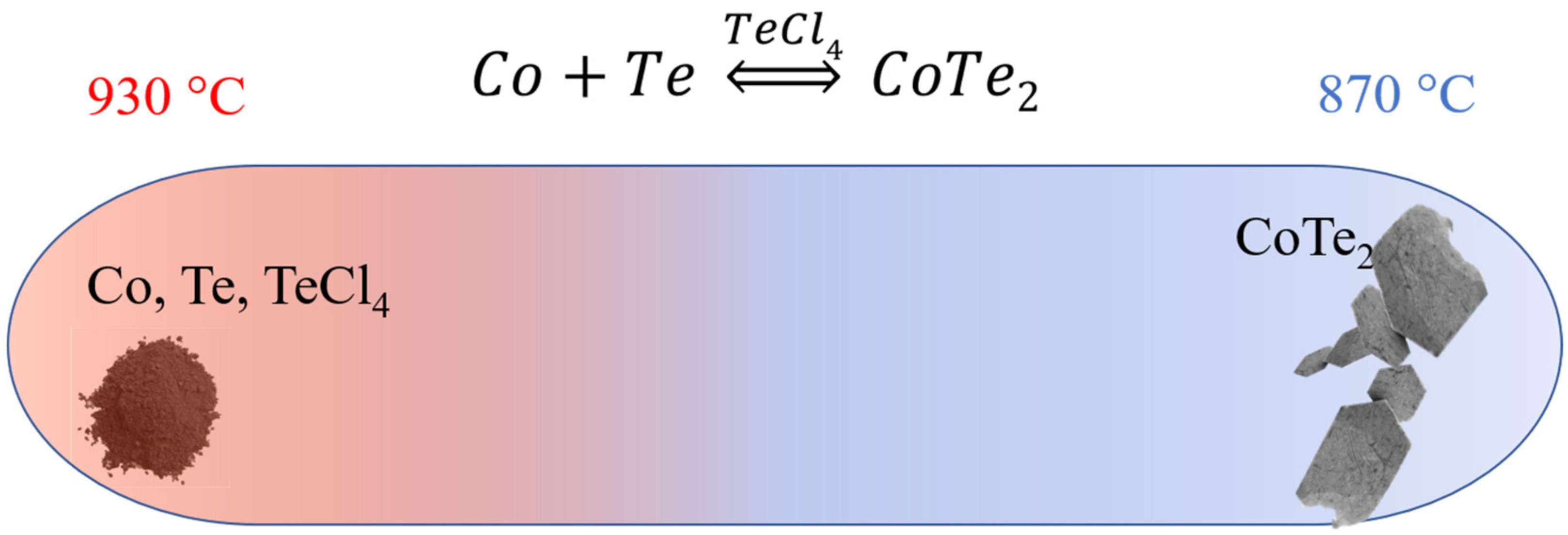
2. Experiments
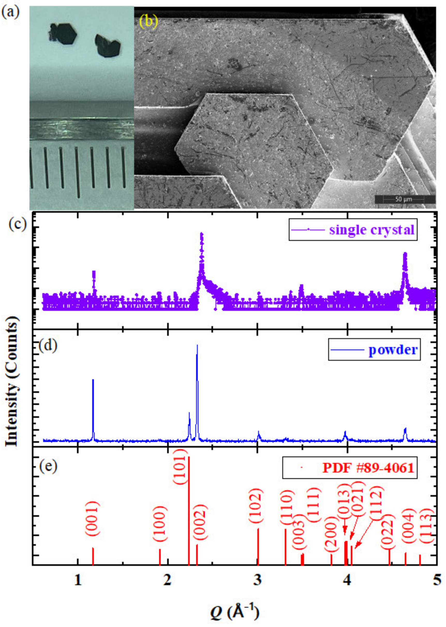
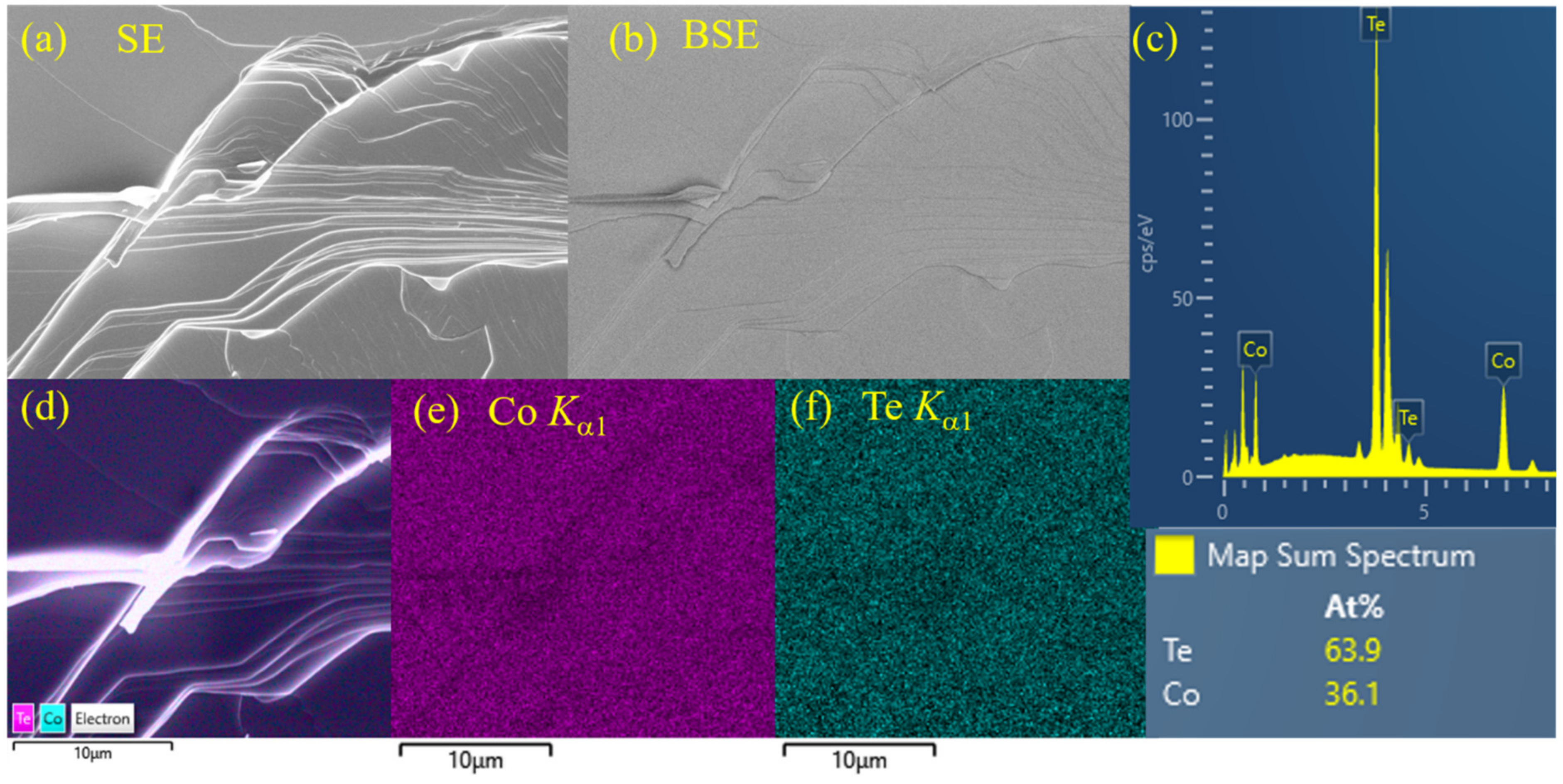
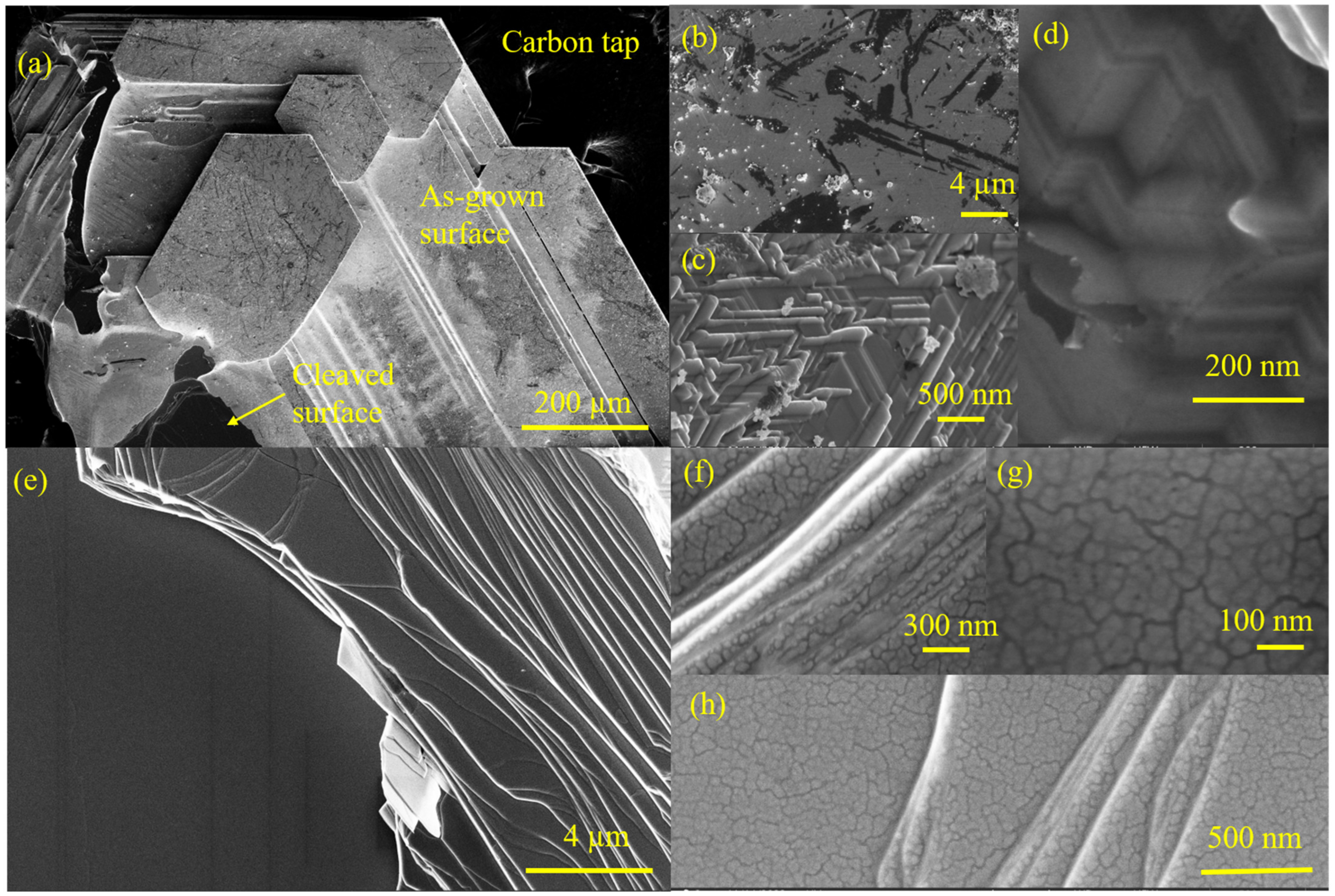
3. Results and Discussion
Author Contributions
Funding
Data Availability Statement
Conflicts of Interest
References
- Novoselov, K.S.; Geim, A.K.; Morozov, S.V.; Jiang, D.; Katsnelson, M.I.; Grigorieva, I.V.; Dubonos, S.; Firsov, A.A. Two-dimensional gas of massless Dirac fermions in graphene. Nature 2005, 438, 197–200. [Google Scholar] [CrossRef]
- Novoselov, K.S.; Geim, A.K.; Morozov, S.V.; Jiang, D.-E.; Zhang, Y.; Dubonos, S.V.; Grigorieva, I.V.; Firsov, A.A. Electric field effect in atomically thin carbon films. Science 2004, 306, 666–669. [Google Scholar] [CrossRef]
- Bernardi, M.; Palummo, M.; Grossman, J.C. Extraordinary Sunlight Absorption and One Nanometer Thick Photovoltaics Using Two-Dimensional Monolayer Materials. Nano Lett. 2013, 13, 3664–3670. [Google Scholar] [CrossRef]
- Kang, K.; Xie, S.E.; Huang, L.J.; Han, Y.M.; Huang, P.Y.; Mak, K.F.; Kim, C.J.; Muller, D.; Park, J. High-mobility three-atom-thick semiconducting films with wafer-scale homogeneity. Nature 2015, 520, 656–660. [Google Scholar] [CrossRef]
- Li, H.; Wu, J.M.T.; Yin, Z.Y.; Zhang, H. Preparation and Applications of Mechanically Exfoliated Single-Layer and Multi layer MoS2 and WSe2 Nanosheets. Acc. Chem. Res. 2014, 47, 1067–1075. [Google Scholar] [CrossRef]
- Liu, W.; Kang, J.H.; Sarkar, D.; Khatami, Y.; Jena, D.; Banerjee, K. Role of Metal Contacts in Designing High-Performance Monolayer n-Type WSe2 Field Effect Transistors. Nano Lett. 2013, 13, 1983–1990. [Google Scholar] [CrossRef]
- Lv, R.; Robinson, J.A.; Schaak, R.E.; Sun, D.; Sun, Y.F.; Mallouk, T.E.; Terrones, M. Transition Metal Dichalcogenides and Beyond: Synthesis, Properties, and Applications of Single- and Few-Layer Nanosheets. Acc. Chem. Res. 2015, 48, 56–64. [Google Scholar] [CrossRef]
- Ugeda, M.M.; Bradley, A.J.; Shi, S.F.; da Jornada, F.H.; Zhang, Y.; Qiu, D.Y.; Ruan, W.; Mo, S.K.; Hussain, Z.; Shen, Z.X.; et al. Giant bandgap renormalization and excitonic effects in a monolayer transition metal dichalcogenide semiconductor. Nat. Mater. 2014, 13, 1091–1095. [Google Scholar] [CrossRef]
- Wang, H.; Yu, L.L.; Lee, Y.H.; Shi, Y.M.; Hsu, A.; Chin, M.L.; Li, L.J.; Dubey, M.; Kong, J.; Palacios, T. Integrated Circuits Based on Bilayer MoS2 Transistors. Nano Lett. 2012, 12, 4674–4680. [Google Scholar] [CrossRef]
- Choi, W.; Ahn, J.; Kim, K.T.; Jin, H.J.; Hong, S.; Hwang, D.K.; Im, S. Ambipolar Channel p-TMD/n-Ga2O3 Junction Field Effect Transistors and High Speed Photo-sensing in TMD Channel. Adv. Mater. 2021, 33, 2103079. [Google Scholar] [CrossRef]
- Kallatt, S.; Umesh, G.; Bhat, N.; Majumdar, K. Photoresponse of atomically thin MoS2 layers and their planar heterojunctions. Nanoscale 2016, 8, 15213–15222. [Google Scholar] [CrossRef]
- Liu, R.; Wang, F.K.; Liu, L.X.; He, X.Y.; Chen, J.Z.; Li, Y.; Zhai, T.Y. Band Alignment Engineering in Two-Dimensional Transition Metal Dichalcogenide-Based Heterostructures for Photodetectors. Small Struct. 2021, 2, 2000136. [Google Scholar] [CrossRef]
- Liu, W.J.; Liu, M.L.; Han, H.N.; Fang, S.B.; Teng, H.; Lei, M.; Wei, Z.Y. Nonlinear optical properties of WSe2 and MoSe2 films and their applications in passive Q-switched erbium doped fiber lasers. Photonics Res. 2018, 6, C15–C21. [Google Scholar] [CrossRef]
- Lu, J.P.; Liu, H.W.; Tok, E.S.; Sow, C.H. Interactions between lasers and two-dimensional transition metal dichalcogenides. Chem. Soc. Rev. 2016, 45, 2494–2515. [Google Scholar] [CrossRef]
- Si, K.Y.; Ma, J.Y.; Lu, C.H.; Zhou, Y.X.; He, C.; Yang, D.; Wang, X.M.; Xu, X.L. A two-dimensional MoS2/WSe2 van der Waals heterostructure for enhanced photoelectric performance. Appl. Surf. Sci. 2020, 507, 145082. [Google Scholar] [CrossRef]
- Zhuang, M.H.; Xu, G.L.; Gan, L.Y.; Dou, Y.B.; Sun, C.J.; Ou, X.W.; Xie, Y.Y.; Liu, Z.J.; Cai, Y.T.; Ding, Y.; et al. Sub-5 nm edge-rich 1T′-ReSe2 as bifunctional materials for hydrogen evolution and sodium-ion storage. Nano Energy 2019, 58, 660–668. [Google Scholar] [CrossRef]
- de la Barrera, S.C.; Sinko, M.R.; Gopalan, D.P.; Sivadas, N.; Seyler, K.L.; Watanabe, K.; Taniguchi, T.; Tsen, A.W.; Xu, X.D.; Xiao, D.; et al. Tuning Ising superconductivity with layer and spin-orbit coupling in two-dimensional transition-metal dichalcogenides. Nat. Commun. 2018, 9, 1427. [Google Scholar] [CrossRef]
- Shi, W.; Ye, J.T.; Zhang, Y.J.; Suzuki, R.; Yoshida, M.; Miyazaki, J.; Inoue, N.; Saito, Y.; Iwasa, Y. Superconductivity Series in Transition Metal Dichalcogenides by Ionic Gating. Sci. Rep. 2015, 5, 12534. [Google Scholar] [CrossRef]
- Sipos, B.; Kusmartseva, A.F.; Akrap, A.; Berger, H.; Forró, L.; Tutis, E. From Mott state to superconductivity in 1T-TaS2. Nat. Mater. 2008, 7, 960–965. [Google Scholar] [CrossRef]
- Zhou, B.T.; Yuan, N.F.Q.; Jiang, H.L.; Law, K.T. Ising superconductivity and Majorana fermions in transition-metal dichalcogenides. Phys. Rev. B 2016, 93, 180501(R). [Google Scholar] [CrossRef]
- Baranowski, M.; Surrente, A.; Klopotowski, L.; Urban, J.M.; Zhang, N.; Maude, D.K.; Wiwatowski, K.; Mackowski, S.; Kung, Y.C.; Dumcenco, D.; et al. Probing the Interlayer Exciton Physics in a MoS2/MoSe2/MoS2 van der Waals Heterostructure. Nano Lett. 2017, 17, 6360–6365. [Google Scholar] [CrossRef]
- Calman, E.V.; Fogler, M.M.; Butov, L.V.; Hu, S.; Mishchenko, A.; Geim, A.K. Indirect excitons in van der Waals heterostructures at room temperature. Nat. Commun. 2018, 9, 1895. [Google Scholar] [CrossRef]
- Epstein, I.; Terres, B.; Chaves, A.J.; Pusapati, V.V.; Rhodes, D.A.; Frank, B.; Zimmermann, V.; Qin, Y.; Watanabe, K.; Taniguchi, T.; et al. Near-Unity Light Absorption in a Monolayer WS2 Van der Waals Heterostructure Cavity. Nano Lett. 2020, 20, 3545–3552. [Google Scholar] [CrossRef]
- Ghiasi, T.S.; Ingla-Aynés, J.; Kaverzin, A.A.; van Wees, B.J. Large Proximity-Induced Spin Lifetime Anisotropy in Transition-Metal Dichalcogenide/Graphene Heterostructures. Nano Lett. 2017, 17, 7528–7532. [Google Scholar] [CrossRef]
- Kim, J.; Jin, C.H.; Chen, B.; Cai, H.; Zhao, T.; Lee, P.; Kahn, S.; Watanabe, K.; Taniguchi, T.; Tongay, S.; et al. Observation of ultralong valley lifetime in WSe2/MoS2 heterostructures. Sci. Adv. 2017, 3, e1700518. [Google Scholar] [CrossRef]
- Regan, E.C.; Wang, D.Q.; Paik, E.Y.; Zeng, Y.X.; Zhang, L.; Zhu, J.H.; MacDonald, A.H.; Deng, H.; Wang, F. Emerging exciton physics in transition metal dichalcogenide heterobilayers. Nat. Rev. Mater. 2022, 7, 778–795. [Google Scholar] [CrossRef]
- Brotons-Gisbert, M.; Baek, H.; Molina-Sanchez, A.; Campbell, A.; Scerri, E.; White, D.; Watanabe, K.; Taniguchi, T.; Bonato, C.; Gerardot, B.D. Spin-layer locking of interlayer excitons trapped in moire potentials. Nat. Mater. 2020, 19, 630–636. [Google Scholar] [CrossRef]
- Choi, J.H.; Hsu, W.T.; Lu, L.S.; Sun, L.Y.; Cheng, H.Y.; Lee, M.H.; Quan, J.M.; Tran, K.; Wang, C.Y.; Staab, M.; et al. Moire potential impedes interlayer exciton diffusion in van der Waals heterostructures. Sci. Adv. 2020, 6, eaba8866. [Google Scholar] [CrossRef]
- Enaldiev, V.V.; Zólyomi, V.; Yelgel, C.; Magorrian, S.J.; Fal’ko, V.I. Stacking Domains and Dislocation Networks in Marginally Twisted Bilayers of Transition Metal Dichalcogenides. Phys. Rev. Lett. 2020, 124, 206101. [Google Scholar] [CrossRef]
- Hennighausen, Z.; Kar, S. Twistronics: A turning point in 2D quantum materials. Electron. Struct. 2021, 3, 014004. [Google Scholar] [CrossRef]
- Li, H.Y.; Li, S.W.; Naik, M.H.; Xie, J.X.; Li, X.Y.; Wang, J.Y.; Regan, E.; Wang, D.Q.; Zhao, W.Y.; Zhao, S.H.; et al. Imaging moire flat bands in three-dimensional reconstructed WSe2/WS2 superlattices. Nat. Mater. 2021, 20, 945–950. [Google Scholar] [CrossRef]
- Maity, I.; Naik, M.H.; Maiti, P.K.; Krishnamurthy, H.R.; Jain, M. Phonons in twisted transition-metal dichalcogenide bilayers: Ultrasoft phasons and a transition from a superlubric to a pinned phase. Phys. Rev. Res. 2020, 2, 013335. [Google Scholar] [CrossRef]
- Marcellina, E.; Liu, X.; Hu, Z.H.; Fieramosca, A.; Huang, Y.Q.; Du, W.; Liu, S.; Zhao, J.; Watanabe, K.; Taniguchi, T.; et al. Evidence for Moire Trions in Twisted MoSe2 Homobilayers. Nano Lett. 2021, 21, 4461–4468. [Google Scholar] [CrossRef]
- Rosenberger, M.R.; Chuang, H.J.; Phillips, M.; Oleshko, V.P.; McCreary, K.M.; Sivaram, S.V.; Hellberg, C.S.; Jonker, B.T. Twist Angle-Dependent Atomic Reconstruction and Moire Patterns in Transition Metal Dichalcogenide Heterostructures. Acs Nano 2020, 14, 4550–4558. [Google Scholar] [CrossRef]
- Ruiz-Tijerina, D.A.; Fal’ko, V.I. Interlayer hybridization and moire superlattice minibands for electrons and excitons in heterobilayers of transition-metal dichalcogenides. Phys. Rev. B 2019, 99, 125424. [Google Scholar] [CrossRef]
- Sung, J.; Zhou, Y.; Scuri, G.; Zólyomi, V.; Andersen, T.I.; Yoo, H.; Wild, D.S.; Joe, A.Y.; Gelly, R.J.; Heo, H.; et al. Broken mirror symmetry in excitonic response of reconstructed domains in twisted MoSe2/MoSe2bilayers. Nat. Nanotechnol. 2020, 15, 750–754. [Google Scholar] [CrossRef]
- Wilson, N.P.; Yao, W.; Shan, J.; Xu, X.D. Excitons and emergent quantum phenomena in stacked 2D semiconductors. Nature 2021, 599, 383–392. [Google Scholar] [CrossRef]
- Xie, Y.M.; Zhang, C.P.; Hu, J.X.; Mak, K.F.; Law, K.T. Valley-Polarized Quantum Anomalous Hall State in Moire MoTe2/WSe2 Heterobilayers. Phys. Rev. Lett. 2022, 128, 026402. [Google Scholar] [CrossRef]
- Ali, M.N.; Xiong, J.; Flynn, S.; Tao, J.; Gibson, Q.D.; Schoop, L.M.; Liang, T.; Haldolaarachchige, N.; Hirschberger, M.; Ong, N.P.; et al. Large, non-saturating magnetoresistance in WTe2. Nature 2014, 514, 205–208. [Google Scholar] [CrossRef]
- Soluyanov, A.A.; Gresch, D.; Wang, Z.J.; Wu, Q.S.; Troyer, M.; Dai, X.; Bernevig, B.A. Type-II Weyl semimetals. Nature 2015, 527, 495–498. [Google Scholar] [CrossRef]
- Yan, M.Z.; Huang, H.Q.; Zhang, K.N.; Wang, E.Y.; Yao, W.; Deng, K.; Wan, G.L.; Zhang, H.Y.; Arita, M.; Yang, H.T.; et al. Lorentz-violating type-II Dirac fermions in transition metal dichalcogenide PtTe2. Nat. Commun. 2017, 8, 257. [Google Scholar] [CrossRef] [PubMed]
- Hasan, M.Z.; Kane, C.L. Colloquium: Topological insulators. Rev. Mod. Phys. 2010, 82, 3045–3067. [Google Scholar] [CrossRef]
- Qi, X.L.; Zhang, S.C. Topological insulators and superconductors. Rev. Mod. Phys. 2011, 83, 1057. [Google Scholar] [CrossRef]
- Zhao, W.; Wang, X. Berry phase in quantum oscillations of topological materials. Adv. Phys. X 2022, 7, 2064230. [Google Scholar] [CrossRef]
- Fu, L.; Kane, C.L. Topological insulators with inversion symmetry. Phys. Rev. B 2007, 76, 045302. [Google Scholar] [CrossRef]
- Fei, Z.Y.; Palomaki, T.; Wu, S.F.; Zhao, W.J.; Cai, X.H.; Sun, B.S.; Nguyen, P.; Finney, J.; Xu, X.D.; Cobden, D.H. Edge conduction in monolayer WTe2. Nat. Phys. 2017, 13, 677–682. [Google Scholar] [CrossRef]
- Tang, S.J.; Zhang, C.F.; Wong, D.; Pedramrazi, Z.; Tsai, H.Z.; Jia, C.J.; Moritz, B.; Claassen, M.; Ryu, H.; Kahn, S.; et al. Quantum spin Hall state in monolayer 1T′-WTe2. Nat. Phys. 2017, 13, 683–687. [Google Scholar] [CrossRef]
- Chia, X.Y.; Adriano, A.; Lazar, P.; Sofer, Z.; Luxa, J.; Pumera, M. Layered Platinum Dichalcogenides (PtS2, PtSe2, and PtTe2) Electrocatalysis: Monotonic Dependence on the Chalcogen Size. Adv. Funct. Mater. 2016, 26, 4306–4318. [Google Scholar] [CrossRef]
- Chia, X.Y.; Sofer, Z.; Luxa, J.; Pumera, M. Unconventionally Layered CoTe2 and NiTe2 as Electrocatalysts for Hydrogen Evolution. Chem. A Eur. J. 2017, 23, 11719–11726. [Google Scholar] [CrossRef]
- Ganesan, V.; Nam, K.H.; Park, C.M. Robust Polyhedral CoTe2-C Nanocomposites as High-Performance Li- and Na-Ion Battery Anodes. ACS Appl. Energy Mater. 2020, 3, 4877–4887. [Google Scholar] [CrossRef]
- Gao, Q.; Huang, C.Q.; Ju, Y.M.; Gao, M.R.; Liu, J.W.; An, D.; Cui, C.H.; Zheng, Y.R.; Li, W.X.; Yu, S.H. Phase-Selective Syntheses of Cobalt Telluride Nanofleeces for Efficient Oxygen Evolution Catalysts. Angew. Chem. -Int. Ed. 2017, 56, 7769–7773. [Google Scholar] [CrossRef] [PubMed]
- Ji, L.; Wang, Z.C.; Wang, H.; Shi, X.F.; Asiri, A.M.; Sun, X.P. Hierarchical CoTe2 Nanowire Array: An Effective Oxygen Evolution Catalyst in Alkaline Media. Acs Sustain. Chem. Eng. 2018, 6, 4481–4485. [Google Scholar] [CrossRef]
- Liu, M.; Lu, X.Q.; Guo, C.; Wang, Z.J.; Li, Y.P.; Lin, Y.; Zhou, Y.; Wang, S.T.; Zhang, J. Architecting a Mesoporous N-Doped Graphitic Carbon Framework Encapsulating CoTe2 as an Efficient Oxygen Evolution Electrocatalyst. ACS Appl. Mater. Interfaces 2017, 9, 36146–36153. [Google Scholar] [CrossRef] [PubMed]
- Lu, T.H.; Chen, C.J.; Basu, M.; Ma, C.G.; Liu, R.S. The CoTe2 nanostructure: An efficient and robust catalyst for hydrogen evolution. Chem. Commun. 2015, 51, 17012–17015. [Google Scholar] [CrossRef] [PubMed]
- Ma, H.F.; Dang, W.Q.; Yang, X.D.; Li, B.; Zhang, Z.W.; Chen, P.; Liu, Y.; Wan, Z.; Qian, Q.; Luo, J.; et al. Chemical Vapor Deposition Growth of Single Crystalline CoTe2 Nanosheets with Tunable Thickness and Electronic Properties. Chem. Mater. 2018, 30, 8891–8896. [Google Scholar] [CrossRef]
- McKendry, I.G.; Thenuwara, A.C.; Sun, J.W.; Peng, H.W.; Perdew, J.P.; Strongin, D.R.; Zdilla, M.J. Water Oxidation Catalyzed by Cobalt Oxide Supported on the Mattagamite Phase of CoTe2. ACS Catal. 2016, 6, 7393–7397. [Google Scholar] [CrossRef]
- Muhler, M.; Bensch, W.; Schur, M. Preparation, crystal structures, experimental and theoretical electronic band structures of cobalt tellurides in the composition range CoTe1.3-CoTe2. J. Phys. -Condens. Matter 1998, 10, 2947–2962. [Google Scholar] [CrossRef]
- Nath, M.; De Silva, U.; Singh, H.; Perkins, M.; Liyanage, W.P.R.; Umapathi, S.; Chakravarty, S.; Masud, J. Cobalt Telluride: A Highly Efficient Trifunctional Electrocatalyst for Water Splitting and Oxygen Reduction. ACS Appl. Energy Mater. 2021, 4, 8158–8174. [Google Scholar] [CrossRef]
- Wang, K.; Ye, Z.G.; Liu, C.Q.; Xi, D.; Zhou, C.J.; Shi, Z.Q.; Xia, H.Y.; Liu, G.W.; Qiao, G.J. Morphology-Controllable Synthesis of Cobalt Telluride Branched Nanostructures on Carbon Fiber Paper as Electrocatalysts for Hydrogen Evolution Reaction. ACS Appl. Mater. Interfaces 2016, 8, 2910–2916. [Google Scholar] [CrossRef]
- Wang, X.; Huang, X.K.; Gao, W.B.; Tang, Y.; Jiang, P.B.; Lan, K.; Yang, R.Z.; Wang, B.; Li, R. Metal-organic framework derived CoTe2 encapsulated in nitrogen-doped carbon nanotube frameworks: A high-efficiency bifunctional electrocatalyst for overall water splitting. J. Mater. Chem. A 2018, 6, 3684–3691. [Google Scholar] [CrossRef]
- Wang, X.G.; Zhou, Z.; Zhang, P.; Zhang, S.Q.; Ma, Y.; Yang, W.W.; Wang, H.; Li, B.X.; Meng, L.J.; Jiang, H.N.; et al. Thickness-Controlled Synthesis of CoX2 (X = S, Se, and Te) Single Crystalline 2D Layers with Linear Magnetoresistance and High Conductivity. Chem. Mater. 2020, 32, 2321–2329. [Google Scholar] [CrossRef]
- Wang, Z.Q.; Ren, X.; Wang, L.; Cui, G.W.; Wang, H.J.; Sun, X.P. A hierarchical CoTe2-MnTe2 hybrid nanowire array enables high activity for oxygen evolution reactions. Chem. Commun. 2018, 54, 10993–10996. [Google Scholar] [CrossRef] [PubMed]
- Yin, Y.Q.; Xu, J.; Guo, W.; Wang, Z.; Du, X.D.; Chen, C.; Zheng, Z.J.; Liu, D.; Qu, D.Y.; Xie, Z.Z.; et al. A single-step fabrication of CoTe2 nanofilm electrode toward efficient overall water splitting. Electrochim. Acta 2019, 307, 451–458. [Google Scholar] [CrossRef]
- Zhang, B.; Zhang, Y.; Li, J.L.; Liu, J.; Huo, X.G.; Kang, F.Y. In situ growth of metal-organic framework-derived CoTe2 nanoparticles@nitrogen-doped porous carbon polyhedral composites as novel cathodes for rechargeable aluminum-ion batteries. J. Mater. Chem. A 2020, 8, 5535–5545. [Google Scholar] [CrossRef]
- Siegfried, P.E.; Bhandari, H.; Qi, J.N.; Ghimire, R.; Joshi, J.; Messegee, Z.T.; Beeson, W.B.; Liu, K.; Ghimire, M.P.; Dang, Y.L.; et al. CoTe2: A Quantum Critical Dirac Metal with Strong Spin Fluctuations. Adv. Mater. 2023, 35, 2300640. [Google Scholar] [CrossRef] [PubMed]
- Wang, B.; Wang, L.; Ding, D.; Zhai, Y.; Wang, F.; Jing, Z.; Yang, X.; Kong, Y.; Qian, Y.; Xu, L. Zinc-Assisted Cobalt Ditelluride Polyhedra Inducing Lattice Strain to Endow Efficient Adsorption-Catalysis for High-Energy Lithium–Sulfur Batteries. Adv. Mater. 2022, 34, 2204403. [Google Scholar] [CrossRef] [PubMed]
- Chakraborty, A.; Fujii, J.; Kuo, C.N.; Lue, C.S.; Politano, A.; Vobornik, I.; Agarwal, A. Observation of highly anisotropic bulk dispersion and spin-polarized topological surface states in CoTe2. Phys. Rev. B 2023, 107, 085406. [Google Scholar] [CrossRef]
- Hu, Z.; Zhang, L.B.; Chakraborty, A.; D’Olimpio, G.; Fujii, J.; Ge, A.P.; Zhou, Y.C.; Liu, C.L.; Agarwal, A.; Vobornik, I.; et al. Terahertz Nonlinear Hall Rectifiers Based on Spin-Polarized Topological Electronic States in 1T-CoTe2. Adv. Mater. 2023, 35, 2209557. [Google Scholar] [CrossRef]
- Guo, L.; Xu, M.; Chen, L.; Huang, X.; Shi, X.Y.; Ying, J.S.; Zhang, T.; Zhao, W.Y.; Dong, S.; Zheng, R.K. Electronic Transport Properties of Nb1-xTaxSb2 Single-Crystal Semimetals Grown by a Chemical Vapor Transport Based High-Throughput Method. Cryst. Growth Des. 2021, 21, 653–662. [Google Scholar] [CrossRef]
- Guo, L.; Zhao, W.Y.; Ding, N.; Shi, X.Y.; Xu, M.; Chen, L.; Gao, G.Y.; Dong, S.; Zheng, R.K. Magnetotransport properties of square-net compounds of NbSiSb and NbGeSb single crystals. J. Phys. Condens. Matter 2020, 32, 435701. [Google Scholar] [CrossRef]
- Wu, J.; Zhang, C.L.; Yan, J.M.; Chen, L.; Guo, L.; Chen, T.W.; Gao, G.Y.; Fei, L.F.; Zhao, W.Y.; Chai, Y.; et al. Magnetotransport and magnetic properties of the layered noncollinear antiferromagnetic Cr2Se3 single crystals. J. Phys. Condens. Matter 2020, 32, 475801. [Google Scholar] [CrossRef] [PubMed]
- Xu, M.; Guo, L.; Chen, L.; Zhang, Y.; Li, S.S.; Zhao, W.Y.; Wang, X.L.; Dong, S.; Zheng, R.K. Emerging weak antilocalization effect in Ta0.7Nb0.3Sb2 semimetal single crystals. Front. Phys. 2023, 18, 13304. [Google Scholar] [CrossRef]
- Zhang, S.J.; Yan, J.M.; Tang, F.; Wu, J.; Dong, W.Q.; Zhang, D.W.; Luo, F.S.; Chen, L.; Fang, Y.; Zhang, T.; et al. Colossal Magnetoresistance in Ti Lightly Doped Cr2Se3 Single Crystals with a Layered Structure. ACS Appl. Mater. Interfaces 2021, 13, 58949–58955. [Google Scholar] [CrossRef] [PubMed]
- Li, Z.; Chen, H.; Jin, S.; Gan, D.; Wang, W.; Guo, L.; Chen, X. Weyl semimetal TaAs: Crystal growth, morphology, and thermodynamics. Cryst. Growth Des. 2016, 16, 1172–1175. [Google Scholar] [CrossRef]
- Liu, Q.; Fei, F.; Chen, B.; Bo, X.; Wei, B.; Zhang, S.; Zhang, M.; Xie, F.; Naveed, M.; Wan, X. Nontopological origin of the planar Hall effect in the type-II Dirac semimetal NiTe2. Phys. Rev. B 2019, 99, 155119. [Google Scholar] [CrossRef]
- Chen, L.; Zhao, W.; Wang, Z.; Tang, F.; Fang, Y.; Zeng, Z.; Xia, Z.; Cheng, Z.; Cortie, D.L.; Rule, K.C. Spin Reorientation Transition and Negative Magnetoresistance in Ferromagnetic NdCrSb3 Single Crystals. Materials 2023, 16, 1736. [Google Scholar] [CrossRef]


Disclaimer/Publisher’s Note: The statements, opinions and data contained in all publications are solely those of the individual author(s) and contributor(s) and not of MDPI and/or the editor(s). MDPI and/or the editor(s) disclaim responsibility for any injury to people or property resulting from any ideas, methods, instructions or products referred to in the content. |
© 2023 by the authors. Licensee MDPI, Basel, Switzerland. This article is an open access article distributed under the terms and conditions of the Creative Commons Attribution (CC BY) license (https://creativecommons.org/licenses/by/4.0/).
Share and Cite
Chen, L.; Zhao, W.; Zheng, R.-K. Single Crystal Growth and Nano-Structure Study in a Topological Dirac Metal, CoTe2-δ. Crystals 2024, 14, 46. https://doi.org/10.3390/cryst14010046
Chen L, Zhao W, Zheng R-K. Single Crystal Growth and Nano-Structure Study in a Topological Dirac Metal, CoTe2-δ. Crystals. 2024; 14(1):46. https://doi.org/10.3390/cryst14010046
Chicago/Turabian StyleChen, Lei, Weiyao Zhao, and Ren-Kui Zheng. 2024. "Single Crystal Growth and Nano-Structure Study in a Topological Dirac Metal, CoTe2-δ" Crystals 14, no. 1: 46. https://doi.org/10.3390/cryst14010046