Article

Probing Boron Vacancy Complexes in h-BN Semi-Bulk Crystals Synthesized by Hydride Vapor Phase Epitaxy

Department of Electrical and Computer Engineering, Texas Tech University, Lubbock, TX 79409, USA
*
Authors to whom correspondence should be addressed.
Crystals 2023, 13(9), 1319; https://doi.org/10.3390/cryst13091319
Submission received: 13 August 2023 / Revised: 25 August 2023 / Accepted: 26 August 2023 / Published: 29 August 2023
(This article belongs to the Special Issue Epitaxial Growth of Semiconductor Materials and Devices)

Abstract

:
Hexagonal BN (h-BN) has emerged as an important ultrawide bandgap (UWBG) semiconductor (Eg~6 eV). The crystal growth technologies for producing semi-bulk crystals/epilayers in large wafer sizes and understanding of defect properties lag decades behind conventional III-nitride wide bandgap (WBG) semiconductors. Here we report probing of boron vacancy (VB)-related defects in freestanding h-BN semi-bulk wafers synthesized by hydride vapor phase epitaxy (HVPE). A photocurrent excitation spectroscopy (PES) was designed to monitor the transport of photoexcited holes from deep-level acceptors. A dominant transition line at 1.66 eV with a side band near 1.62 eV has been directly observed, which matches well with the calculated energy levels of 1.65 for the VB-H deep acceptor in h-BN. The identification of VB complexes via PES measurement was further corroborated by the temperature-dependent dark resistivity and secondary ion mass spectrometry measurements. The results presented here suggested that it is necessary to focus on the optimization of V/III ratio during HVPE growth to minimize the generation of VB-related defects and to improve the overall material quality of h-BN semi-bulk crystals. The work also provided a better understanding of how VB complexes behave and affect the electronic and optical properties of h-BN.

1. Introduction

III-nitride wide bandgap (WBG) semiconductors have revolutionized the consumer electronics and lighting industries [1,2,3] and are also making inroads in power electronics and full-spectrum solar energy conversion applications [4,5,6]. In the development of III-nitride WBG semiconductors, how to achieve electrical conductivity control was a critical issue because many important devices rely on the ability of n- and p-type doping. The properties of Ga vacancy (VGa) in GaN have been discussed and investigated throughout the development history of III-nitrides. In terms of its effect on the optical properties of GaN, the presence of a Ga vacancy complex with a double negatively charged state (VGa-complex)−2 was thought to be the origin of the yellow line (YL) at about 2.2 eV [7,8,9,10,11,12,13,14,15,16,17]. More recently, the acceptor involving a substitutional carbon on nitrogen site (CN) being the source of the YL in GaN has also been proposed [15]. In terms of its effects on the electrical properties, VGa and (VGa-complex) are deep-level acceptors, and they can capture electrons. While YL in GaN was extensively studied, the violet line (VL) appearing at around 3.4 eV in AlN related to the presence of Al vacancies (VAl) is less well known. Theoretical calculations revealed that the formation energy of VIII in AlGaN decreases with increasing Al-content and becomes very low forming a triple negatively charged state in AlN ( V A l 3 ) [7,16,17]. As a direct consequence, achieving n-type conductivity control in AlGaN alloys with high Al-contents was challenging because each V A l 3 can trap three electrons. It was clearly shown that the nature of an effective mass state of Si donors can be revealed and highly conductive Al-rich AlGaN alloys can be achieved only after VIII has been suppressed [10,18].
Among III-nitrides, h-BN is quite unique. In addition, its ultrawide bandgap (UWBG) of ~6.0 eV [19,20,21] makes it attractive for deep ultraviolet (UV) photonic devices [22]. Its atomic constituent B-10 has a large thermal neutron capture cross-section [23,24,25,26,27,28], a distinctive property that makes h-BN an excellent material for realizing direct-conversion thermal neutron detectors with a theoretical detection efficiency of 100% possible [27,28]. Its outstanding chemical and thermal properties [29,30,31], together with its UWBG imply that h-BN potentially is also an excellent next-generation electronic material. In its 2D forms, native defects, related to boron vacancy (VB) in h-BN, appear to be excellent single photon emitters [32,33,34].
The properties of native defects and impurities in h-BN have been studied using density functional theory [35]. The results indicated that VB-hydrogen complexes form deep-level acceptors and have a (0/−) charge state [35]. Comparatively, there have been several experimental studies concerning the behaviors of silicon, carbon, and oxygen impurities in h-BN [36,37,38]. The energy level of Si donors in h-BN appears rather deep at around 1.2 eV [36,39]. Oxygen in h-BN occupies the nitrogen site and is a donor with a measured energy level of 0.56 eV [38] and a calculated energy level of 0.6 eV [35]. The presence of oxygen impurities was attributed to oxygen diffusion from the sapphire substrate because higher growth temperatures are required for h-BN than those of AlN and GaN. As of today, while thermal neutron detectors fabricated from 100 μm thick B-10 enriched h-BN (h-10BN) wafers have attained a record high detection efficiency of η = 59% among all solid-state detectors [28], they still fall short of the theoretical efficiency of 88% expected from h-10BN wafers with a thickness of t = 100 μm, according to η = 1 − e−t/λ, where the absorption length (λ) of thermal neutrons in h-10BN is λ = 47.3 μm [27,28]. It is expected that the presence of native defects profoundly affects the performance of h-BN devices as they are charge carrier traps and scattering centers and play a big role in limiting the charge collection efficiency and hence the total efficiency of h-BN detectors.
Previously, a photocurrent excitation spectroscopy (PES) measurement technique was employed to determine the minimum direct energy bandgap of h-BN [40], which together with the energy levels of O donors (measured in ref. [38]) and VB-hydrogen complexes (VB-2H/VB-H) (calculated in ref. [35]) offered a modified energy diagram to capture the unique band edge structure and its associated dominant impurities/defects in h-BN [40]. However, direct observation of VB-2H and VB-H complexes in h-BN by an experimental technique has not been reported. In this work, we report the probing of boron vacancy (VB)-related defects in freestanding h-BN semi-bulk wafers synthesized by hydride vapor phase epitaxy (HVPE). A photocurrent excitation spectroscopy was designed to monitor the transport of photoexcited holes from VB-related deep-level acceptors. The measured energy levels of VB-complexes agree well with those of theoretical prediction. The properties of VB and complexes are also compared with their equivalents in GaN and AlN. The results reported here, together with what we have already learned from AlGaN, provided important insights for an improved understanding of defects/impurities in h-BN.

2. Materials and Methods

The h-BN semi-bulk wafers used in this study were produced by HVPE. Natural boron trichloride (BCl3) and NH3 were used as precursors for B and N, respectively, and H2 was used as a carrier gas [41]. The growth was conducted on a c-plane sapphire of 2-inches in diameter. In contrast to the metal-organic chemical vapor deposition (MOCVD) growth technique, the precursors used in HVPE growth contain no carbon impurities and it provides a faster growth rate than MOCVD. Due to h-BN’s layered structure, a thick h-BN wafer self-separates from the sapphire substrate after growth during the process of cooling down, from which a freestanding h-BN wafer was obtained [28,38,40,41,42]. A micrograph of a representative freestanding h-BN wafer of 2-inches in diameter is shown in Figure 1a. Figure 1b shows an X-ray diffraction (XRD) spectrum in θ-2θ scan, which reveals a single (002) peak at 26.70 and a c-lattice constant of 6.67 Å associated with the hexagonal phase of BN. The turbostratic- (t-) phase of BN, which is often observable at around 260 in MOCVD-grown thick wafers [42] is completely absent in Figure 1b, reflecting an improved crystalline quality and ordering in the c-direction over those of MOCVD-grown h-BN thick wafers reported earlier by our group [42]. However, the full width at half-maximum (FWHM) of the (002) plane of 0.280 (~1000 arcsec) is still broader than those of AlN wafers produced by MOCVD [27]. Moreover, the true c-lattice constant of h-BN bulk crystal is 6.66 Å. The XRD results shown in Figure 1b indicate that the h-BN semi-bulk wafers do not yet possess a perfect crystalline structure and further improvements are still needed. Benchmarking XRD results of h-BN against those of state-of-the-art AlN epilayers with a comparable bandgap and true bulk h-BN serves as a good guideline to further improve the overall crystalline quality of h-BN via reducing the linewidth and shifting the peak position of the h-BN (002) diffraction peak towards the larger angles.
For the electrical property characterization, as illustrated in Figure 2a, a lateral device was fabricated from a diced piece of freestanding h-BN. The detailed device processing procedures have been described previously [41]. The utilization of a lateral geometry is based on the fact that the lateral transport properties of h-BN are superior to its vertical transport properties [27,28,41]. Ohmic contacts consisting of a bi-layer of Ni (100 nm)/Au (40 nm) were deposited on the two edges of the h-BN sample using e-beam evaporation via a mask, leaving ~100 µm of metal overlapping the sample edges. Wire bonding was then performed to electrically connect the deposited metal contacts to the pads of a semiconductor device package. Figure 2b is a micrograph of a fabricated detector with 1.3 mm in width and 10 mm in length. A broad light source covering the wavelength range between 170 and 2100 nm together with a monochromator was used as a variable wavelength excitation source. For photoluminescence (PL) measurements, an excimer laser of wavelength 193 nm was used as an excitation source.

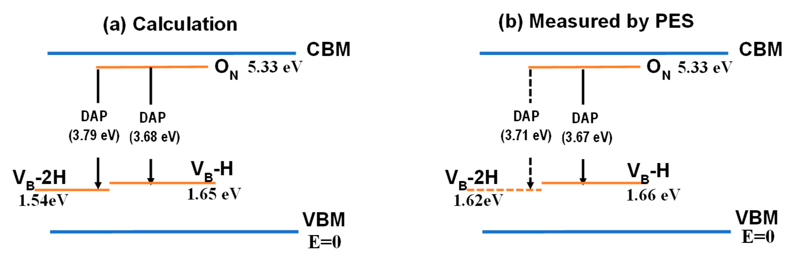
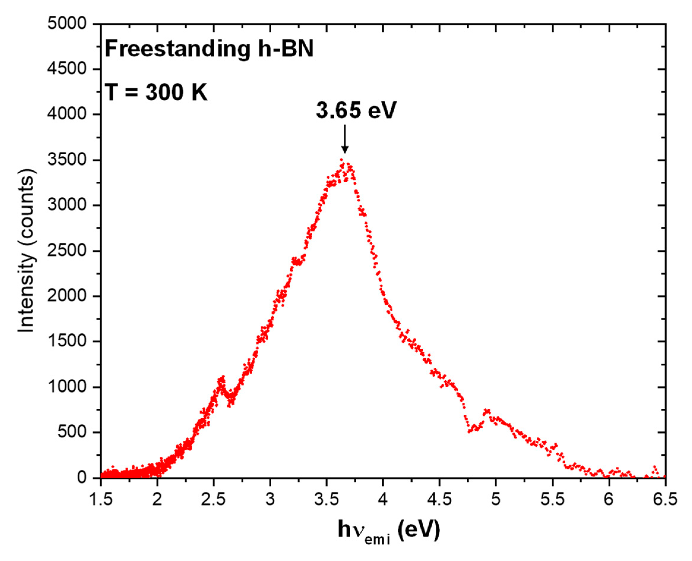
3. Results and Discussion

First, we conducted electrical resistivity (ρ) measurements at varying temperatures. Figure 2c is an Arrhenius plot of the measured temperature-dependent ρ. The inset are plots of dark I-V characteristics measured at several representative temperatures. The resistivity at room temperature is ~1 × 10¹⁴ Ω.cm. The energy level of the impurity/defect which determines the dark resistivity can be estimated from Figure 2c and is ~1.6 eV. We were unable to conduct Hall-effect measurements due to the extremely high resistivity of the material. As such, the energy level estimated here does not include the temperature dependence of the carrier mobility. It is worth noting that the dark I–V characteristics at higher temperatures of 650 K and 700 K are not perfectly linear. This is because the ohmic contacts on h-BN are not optimized and no post-thermal annealing processes were employed. Achieving high-quality ohmic contacts to a new UWBG semiconductor is another challenging research topic and much more work is needed. However, we believe that the results shown in Figure 2c provide a reasonable estimate of the energy level of the impurity/defect involved. Overall, the energy level obtained from the dark resistivity measurements is very close to the calculated energy levels of VB-2H and VB-H complexes, which are predicted to be deep-level acceptors in h-BN [35]. It is also interesting to compare with the results of MOCVD-grown wafers, in which the dark current (or the background carrier concentration) is generally controlled by the presence of oxygen impurities, which are donors with a measured activation energy of about 0.56 eV [38].
To directly probe the presence of VB-2H and VB-H complexes, photocurrent excitation spectroscopy measurement technique was employed, which is a powerful technique for measuring the impurity/defect energy levels and direct energy bandgap in a semiconductor. Photocurrent generation involves a two-step process: (1) direct excitation of carriers from the impurity/defect levels to a band and (2) photoexcited carriers drift in the applied field and collected by the electrodes. Therefore, the observed spectral peak positions in a photocurrent excitation spectrum directly correspond to the impurity/defect energy levels in a semiconductor.
The photocurrent excitation spectroscopy measurement setup is schematically shown in the inset of Figure 3. In this experimental setup, a 300 µm wide metal slit was used to allow light to enter and illuminate only near the metal contact on the left side of the detector strip. Under a bias voltage application with a polarity shown in the inset, only photoexcited free holes (h+) will be able to drift across the detector and be collected by the electrode on the right. Figure 3 plots the measured photocurrent excitation spectrum in the excitation photon energy range of 1.55 and 1.75 eV. Shown in Figure 3 is a dominant spectral peak at 1.66 eV. Another peak observed near 1.65 eV could be due to a phonon replica related to a defect-induced local breathing mode of about 8 meV [43]. Because we are measuring the hole transport, the dominant spectral peak must correspond to the photoexcitation of acceptor impurities/defects with an energy level at EA = 1.66 eV above the valence band. The measured energy level of 1.66 eV matches well with the calculated energy level of 1.65 for the VB-H deep acceptor in h-BN [35]. There appears to be another weak peak near 1.62 eV, possibly associated with the VB-2H deep acceptor in h-BN. However, the observed value of 1.62 eV is not a perfect match with the calculated energy level of 1.54 eV for VB-2H in h-BN [35] and the signal is also near the noise level. The value of EA = 1.6 eV obtained from the dark resistivity measurement results shown in Figure 2 can be considered as the average of the two energy levels among VB-H and VB-H deep acceptors. These results together reinforce that the VB-hydrogen complexes are the dominant acceptor-type defects in h-BN semi-bulk crystals produced by HVPE.
To further confirm the presence of VB-hydrogen complexes in the h-BN wafer studied here, we examined the stoichiometry by secondary ion mass spectrometry (SIMS) measurements to assess the possibility of the presence of native defects of either boron vacancies (VB) or nitrogen vacancies (VN). The choice of using the SIMS technique over other more common surface-sensitive techniques such as X-ray photoelectron spectroscopy (XPS) for this study is because the h-BN surface is prone to oxidation [44] without a proper treatment which can result in misinterpretation of XPS data, whereas SIMS is capable to probe into the sample’s interior. Figure 4 shows B and N concentrations, [B] and [N], in the same h-BN wafer, probed by SIMS. At first sight, SIMS results in Figure 4 hardly reveal any difference between B and N concentrations. We therefore calculated the ratio of [B]/[N] by averaging data points in the wafer’s interior, which revealed that the boron concentration is slightly less than the N concentration with a ratio of boron to nitrogen, [B]/[N] of 49.8/50.2. Knowing that the atomic density of h-BN is 1.1 × 10²³/cm3, this small deficiency in B content (0.2%) could potentially render a concentration of VB and its complex on the order of ~1020 cm−3. This defect concentration is expected to have a significant effect on the device performance since the typical doping levels in p-n junction devices are normally below 1019 cm−3.
The properties and energy levels of various defects and impurities in h-BN have been theoretically investigated [35], which revealed that VB-2H and VB-H complexes are deep-level acceptors in h-BN with their energy positions located respectively at 1.54 and 1.65 eV above the valence band [35]. Because the results of Figure 3 are for hole transport and SIMS data also imply that the h-BN wafer used in this study is slightly boron deficient, comparing the measured acceptor energy level to the calculated energy level of VB-H confirms that the nature of the acceptors with energy levels in the range of 1.6–1.7 eV observed in Figure 3 is VB-complexes. Figure 5 summarizes the energy levels of the deep-level acceptors related to VB-H and VB-2H obtained by (a) calculation [35] and (b) photocurrent excitation spectroscopy measurements here.
Our results lead to several implications and understandings. First, the presence of ON donors with a concentration of [ND] due to oxygen diffusion from sapphire is expected in the material system. However, these donors have been completely compensated by [VB-complex]. This argument can be understood because we are measuring the photocurrent excitation spectrum of free holes, which can only be excited via the photoexcitation process of A0 + hν → A + h+. This means that free holes contributed to the photocurrent excitation spectrum can only be photo-generated by exciting electrons from the valence band to the neutral [VB-complex]0 leaving behind free holes in the valance band. No free holes can be photo-excited at this energy from the negatively charged acceptors. Therefore, [ND] due to oxygen must be less than [VB-complex] to observe this photoexcitation process. All ND will become positively charged donors with [ND+] = [ND] = [VB-complex]-, whereas [VB-complex] + [VB-complex]0 = [VB-complex]. Secondly, holes act as the majority charge carriers in the dark as well as under photoexcitation in h-BN samples studied here, in contrast to MOCVD-grown h-BN thick wafers in which electrons tend to act as the majority carriers because oxygen was found to be the dominant impurities [38]. As such, the Fermi level of the system should be closer to the valence band than the conduction band. Lastly, based on the energy level diagram shown in Figure 5, photoluminescence (PL) emission lines in the photon energy range of 3.6–3.8 eV due to donor-acceptor pair (DAP) recombination are possible. To investigate this possibility, room temperature PL emission spectroscopy measurements were carried out. Figure 6 shows a representative PL emission spectrum, which indeed reveals a dominant emission line near 3.65 eV, which agrees remarkably well with the expected emission energy of 3.67 eV (solid vertical arrow) from Figure 5b. The broadness of the PL emission spectrum is a typical characteristic of a DAP transition. Moreover, the dominant DAP transition in h-BN is usually accompanied by many phonon replicas [45], although they are not clearly resolved in the case here. The observation of the dominant emission being related to a DAP recombination in h-BN semi-bulk crystals also indicates the overall material quality is still some distance away from those of the state-of-the-art conventional III-nitride such as GaN and AlN as well as from those of thin h-BN epitaxial layers [27]. We need to focus on pushing the XRD h-BN (002) diffraction peak in 2θ scan to an even larger angle so that the c-lattice constant approaches the true bulk value of 6.66 Å and the PL spectrum is dominated by the band edge emission lines [27].
Now, let us return to look at the overall picture of cation vacancy-related deep-level acceptors in III-nitride semiconductors. Due to the difference in the crystalline structures between h-BN and AlN with a comparable bandgap, there are some interesting and stark differences between the properties of cation vacancy-related defects in these materials. The dominant cation vacancy in AlN is VAl, whereas the most dominant cation vacancy-related defects in h-BN are VB-H and VB-2H complexes. The dominant charge state of the VAl deep-level acceptor in AlN is (−3), while that in h-BN is (0/−1), suggesting that the detrimental effects of VB–complexes to the n-type doping in h-BN are less severe than those of V A l 3 to the n-type doping in AlN, if an effective mass shallow donor can be identified for h-BN. In terms of their effects on the optical properties, deep-level transitions involving cation vacancies and complexes in AlGaN alloys and their implications to the UV optoelectronic devices based on AlGaN alloys have been systematically studied [7,8,9,10,11,12,13,14,15,16,17,18], whereas similar studies for h-BN are still needed. For device applications such as power electronic devices, UV emitters and detectors, and neutron detectors, VB-related defects not only act as electron traps but also affect the device’s quantum efficiency by acting as charge scattering centers.

4. Conclusions

In summary, a photocurrent excitation spectroscopy of hole transport has been employed to study the photoexcitation of deep-level acceptors in h-BN semi-bulk wafers produced by HVPE. A dominant transition line at 1.66 eV above the valence band has been detected, which agrees well with the calculated energy levels of 1.65 eV for VB-H deep acceptors in h-BN. Both the temperature-dependent dark I-V characteristics revealing a defect/impurity with an activation energy of 1.6 eV and SIMS measurement revealing a slight boron deficiency further supported the photocurrent excitation spectroscopy results. Our results suggested that the key to further improving the material quality of h-BN semi-bulk crystals is to minimize the generation of VB-related defects via optimization of V/III ratio during HVPE growth. Similar to the developments of GaN and AlN in the past, achieving defect-free h-BN is highly challenging in the near future and therefore, it is important to gain a better understanding of how defects such as B vacancies and complexes behave and affect the electronic properties of h-BN.

Author Contributions

Conceptualization, H.J. and J.L. (Jingyu Lin); methodology, Z.A., A.T., J.L. (Jing Li), J.L. (Jingyu Lin) and H.J.; software, J.L. (Jing li); validation, Z.A., A.T., J.L. (Jing Li), J.L. (Jingyu Lin) and H.J.; formal analysis, Z.A., A.T., J.L. (Jing Li), J.L. (Jingyu Lin) and H.J.; investigation, Z.A., A.T. and J.L. (Jing Li); resources, H.J. and J.L. (Jingyu Lin); data curation, Z.A. and A.T.; writing—original draft preparation, J.L. (Jingyu Lin) and H.J.; writing—review and editing, J.L. (Jingyu Lin) and H.J.; visualization, Z.A., A.T., J.L. (Jing Li), J.L. (Jingyu Lin) and H.J.; supervision, H.J., J.L. (Jingyu Lin) and J.L. (Jing Li); project administration, H.J. and J.L. (Jingyu Lin); funding acquisition, H.J. and J.L. (Jingyu Lin). All authors have read and agreed to the published version of the manuscript.

Funding

Advanced Research Projects Agency-Energy: DE-AR0001552.

Data Availability Statement

The data that support the findings of this study are available within the article.

Acknowledgments

The research is supported by DOE ARPA-E (DE-AR0001552) monitored by Olga Spahn and Eric Carlson. Jiang and Lin are grateful to the AT&T Foundation for the support of Ed Whitacre and Linda Whitacre endowed chairs.

Conflicts of Interest

The authors have no conflict to disclose.

References

  1. The Nobel Prize in Physics 2014. Available online: https://www.nobelprize.org/prizes/physics/2014/press-release/ (accessed on 18 August 2023).
  2. Nakamura, S.; Pearton, S.J.; Fasol, G. The Blue Laser Diode. Springer: Berlin/Heidelberg, Germany, 2000. [Google Scholar] [CrossRef]
  3. Jiang, H.X.; Lin, J.Y. How we made the microLED. Nat. Electron. 2023, 6, 257. [Google Scholar] [CrossRef]
  4. Amano, H.; Baines, Y.; Beam, E.; Borga, M.; Bouchet, T.; Chalker, P.R.; Charles, M.; Chen, K.J.; Chowdhury, N.; Chu, R.; et al. The 2018 GaN power electronics roadmap. J. Phys. D Appl. Phys. 2018, 51, 163001. [Google Scholar] [CrossRef]
  5. Wu, J.; Walukiewicz, W.; Yu, K.M.; Ager III, J.W.; Haller, E.E.; Lu, H.; Schaff, W.J.; Saito, Y.; Nanishi, Y. Unusual properties of the fundamental band gap of InN. Appl. Phys. Lett. 2002, 80, 3967. [Google Scholar] [CrossRef]
  6. Kibria, M.G.; Nguyen, H.P.; Cui, K.; Zhao, S.; Liu, D.; Guo, H.; Trudeau, M.L.; Paradis, S.; Hakima, A.R.; Mi, Z. One-step overall water splitting under visible light using multiband InGaN/GaN nanowire heterostructures. ACS Nano 2013, 7, 7886. [Google Scholar] [CrossRef] [PubMed]
  7. Mattila, T.; Nieminen, R.M. Point-defect complexes and broadband luminescence in GaN and AlN. Phys. Rev. B 1997, 55, 9571. [Google Scholar] [CrossRef]
  8. Schubert, E.F.; Goepfert, I.D.; Redwing, J.M. Evidence of compensating centers as origin of yellow luminescence in GaN. Appl. Phys. Lett. 1997, 71, 3224. [Google Scholar] [CrossRef]
  9. Reshchikov, M.A.; Morkoç, H. Luminescence properties of defects in GaN. J. Appl. Phys. 2005, 97, 061301. [Google Scholar] [CrossRef]
  10. Nakarmi, M.L.; Kim, K.H.; Zhu, K.; Lin, J.Y.; Jiang, H.X. Transport properties of highly conductive n-type Al-rich AlxGa1−xN (x ≥ 0.7). Appl. Phys. Lett. 2004, 85, 3769. [Google Scholar] [CrossRef]
  11. Morkoc, H. Comprehensive characterization of hydride VPE grown GaN layers and templates. Mater. Sci. Eng. 2001, 33, 135–207. [Google Scholar] [CrossRef]
  12. Nam, K.B.; Nakarmi, M.L.; Lin, J.Y.; Jiang, H.X. Deep impurity transitions involving cation vacancies and complexes in AlGaN alloys. Appl. Phys. Lett. 2005, 86, 222108. [Google Scholar] [CrossRef]
  13. Reshchikov, M.A.; McNamara, J.D.; Zhang, F.; Monavarian, M.; Usikov, A.; Helava, H.; Makarov, Y.; Morkoç, H. Zero-phonon line and fine structure of the yellow luminescence band in GaN. Phys. Rev. B 2016, 94, 035201. [Google Scholar] [CrossRef]
  14. Matys, M.; Adamowicz, B. Mechanism of yellow luminescence in GaN at room temperature. J. Appl. Phys. 2017, 121, 065104. [Google Scholar] [CrossRef]
  15. Reshchikov, M.A. On the origin of the yellow luminescence band in GaN. Phys. Status Solidi B 2022, 2200488. [Google Scholar] [CrossRef]
  16. Van de Walle, C.G.; Neugebauer, J. First-principles calculations for defects and impurities: Applications to III-nitrides. J. Appl. Phys. 2004, 95, 3851. [Google Scholar] [CrossRef]
  17. Stampfl, C.; Van de Walle, C.G. Doping of AlxGa1−xN. Appl. Phys. Lett. 1998, 72, 459. [Google Scholar] [CrossRef]
  18. Ahmad, H.; Engel, Z.; Matthews, C.M.; Lee, S.; Doolittle, W.A. Realization of homojunction PN AlN diodes. J. Appl. Phys. 2022, 131, 175701. [Google Scholar] [CrossRef]
  19. Arnaud, B.; Lebe, S.; Rabiller, P.; Alouani, M. Huge excitonic effects in layered hexagonal boron nitride. Phys. Rev. Lett. 2006, 96, 026402. [Google Scholar] [CrossRef]
  20. Sugino, T.; Tanioka, K.; Kawasaki, S.; Shirafuji, J. Characterization and field emission of sulfur-doped boron nitride synthesized by plasma-assisted chemical vapor deposition. Jpn. J. Appl. Phys. 1997, 36 Pt 2, L463. [Google Scholar] [CrossRef]
  21. Cassabois, G.; Valvin, P.; Gil, B. Hexagonal boron nitride is an indirect bandgap semiconductor. Nat. Photonics 2016, 10, 262. [Google Scholar] [CrossRef]
  22. Watanabe, K.; Taniguchi, T.; Kanda, H. Far-ultraviolet plane-emission handheld device based on hexagonal boron nitride. Nat. Photonics 2009, 3, 591–594. [Google Scholar] [CrossRef]
  23. Knoll, G.F. Radiation Detection and Measurement, 4th ed.; John Wiley & Sons: Hoboken, NJ, USA, 2010. [Google Scholar]
  24. Osberghaus, O. Die isotopenhäufigkeit des bors. massenspektrometrische untersuchung der elektronenstoßprodukte von BF3 und BCl3. Zeitschrift Fuer Physik 1950, 128, 366. [Google Scholar] [CrossRef]
  25. Lunca-Popa, P.; Brand, J.I.; Balaz, S.; Rosa, L.G.; Boag, N.M.; Bai, M.; Robertson, B.W.; Dowben, P.A. Evidence for multiple polytypes of semiconducting boron carbide (C2B10) from electronic structure. J. Phys. D App. Phys. 2005, 38, 1248. [Google Scholar] [CrossRef]
  26. Nikolic, R.J.; Conway, A.M.; Reinhardt, C.E.; Graff, R.T.; Wang, T.F.; Deo, N.; Cheung, C.L. 6:1 aspect ratio silicon pillar based thermal neutron detector filled with 10B. Appl. Phys. Lett. 2008, 93, 133502. [Google Scholar] [CrossRef]
  27. Maity, A.; Grenadier, S.J.; Li, J.; Lin, J.Y.; Jiang, H.X. Hexagonal boron nitride: Epitaxial growth and device applications. Prog. Quantum. Electron. 2021, 76, 100302. [Google Scholar] [CrossRef]
  28. Maity, A.; Grenadier, S.J.; Li, J.; Lin, J.Y.; Jiang, H.X. High efficiency hexagonal boron nitride neutron detectors with 1 cm2 detection areas. Appl. Phys. Lett. 2020, 116, 142102. [Google Scholar] [CrossRef]
  29. Khatami, M.M.; Van de Put, M.L.; Vandenberghe, W.G. First-principles study of electronic transport in germanane and hexagonal boron nitride. Phys. Rev. B 2001, 104, 235424. [Google Scholar] [CrossRef]
  30. Liu, Z.; Gong, Y.; Zhou, W.; Ma, L.; Yu, J.; Idrobo, J.C.; Jung, J.; MacDonald, A.H.; Vajtai, R.; Lou, J.; et al. Ultrathin high-temperature oxidation-resistant coatings of hexagonal boron nitride. Nat. Commun. 2013, 4, 2541. [Google Scholar] [CrossRef] [PubMed]
  31. Yuan, C.; Li, J.; Lindsay, L.; Cherns, D.; Pomeroy, J.W.; Liu, S.; Edgar, J.H.; Kuball, M. Modulating the thermal conductivity in hexagonal boron nitride via controlled boron isotope concentration. Commun. Phys. 2019, 2, 43. [Google Scholar] [CrossRef]
  32. Bourrellier, R.; Meuret, S.; Tararan, A.; Stephan, O.; Kociak, M.; Tizei, L.H.G.; Zobelli, A. Bright UV single photon emission at point defects in h-BN. Nano Lett. 2016, 16, 4317. [Google Scholar] [CrossRef]
  33. Vuong, T.Q.P.; Cassabois, G.; Valvin, P.; Ouerghi, A.; Chassagneux, Y.; Voisin, C.; Gil, B. Phonon-Photon Mapping in a Color Center in Hexagonal Boron Nitride. Phys. Rev. Lett. 2016, 117, 097402. [Google Scholar] [CrossRef] [PubMed]
  34. Tran, T.; Bray, K.; Ford, M.J.; Toth, M.; Aharonovich, I. Quantum emission from hexagonal boron nitride monolayers. Nat. Nanotechnol. 2016, 11, 37. [Google Scholar] [CrossRef]
  35. Weston, L.; Wickramaratne, D.; Mackoit, M.; Alkauskas, A.; Van de Walle, C.G. Native point defects and impurities in hexagonal boron nitride. Phys. Rev. B 2018, 97, 214104. [Google Scholar] [CrossRef]
  36. Majety, S.; Doan, T.C.; Li, J.; Lin, J.Y.; Jiang, H.X. Electrical transport properties of Si-doped hexagonal boron nitride epilayers. AIP Adv. 2013, 3, 122116. [Google Scholar] [CrossRef]
  37. Uddin, M.R.; Li, J.; Lin, J.Y.; Jiang, H.X. Probing carbon impurities in hexagonal boron nitride epilayers. Appl. Phys. Lett. 2017, 110, 182107. [Google Scholar]
  38. Grenadier, S.J.; Maity, A.; Li, J.; Lin, J.Y.; Jiang, H.X. Origin and roles of oxygen impurities in hexagonal boron nitride epilayers. Appl. Phys. Lett. 2018, 112, 162103. [Google Scholar] [CrossRef]
  39. Oba, F.; Togo, A.; Tanaka, I.; Watanabe, K.; Taniguchi, T. Doping of hexagonal boron nitride via intercalation: A theoretical prediction. Phys. Rev. B 2010, 81, 075125. [Google Scholar] [CrossRef]
  40. Grenadier, S.J.; Maity, A.; Li, J.; Lin, J.Y.; Jiang, H.X. Effects of unique band structure of h-BN probed by photocurrent excitation spectroscopy. Appl. Phys. Express 2022, 15, 051005. [Google Scholar] [CrossRef]
  41. Alemoush, Z.; Hossain, N.K.; Tingsuwatit, A.; Almohammad, M.; Li, J.; Lin, J.Y.; Jiang, H.X. Toward achieving cost-effective hexagonal BN semi-bulk crystals and BN neutron detectors via halide vapor phase epitaxy. Appl. Phys. Lett. 2023, 122, 012105. [Google Scholar] [CrossRef]
  42. McKay, M.A.; Li, J.; Lin, J.Y.; Jiang, H.X. Anisotropic index of refraction and structural properties of hexagonal boron nitride epilayers probed by spectroscopic ellipsometry. J. Appl. Phys. 2020, 127, 0531032. [Google Scholar] [CrossRef]
  43. Fiore, S.; Klinkert, C.; Ducry, F.; Backman, J.; Luisier, M. Influence of the hBN dielectric layers on the quantum transport properties of mos2 transistors. Materials 2022, 15, 1062. [Google Scholar] [CrossRef]
  44. Wang, Q.W.; Li, J.; Lin, J.Y.; Jiang, H.X. Probing the surface oxidation process in hexagonal boron nitride epilayers. AIP Adv. 2020, 10, 025213. [Google Scholar] [CrossRef]
  45. Vokhmintse, A.; Weinstein, I.; Zamyatin, D. Electron-phonon interactions in subband excited photoluminescence of hexagonal boron nitride. J. Lumines 2019, 208, 363. [Google Scholar] [CrossRef]
Figure 1. (a) A micrograph of a 100 μm thick freestanding h-BN wafer of 2-inches in diameter. (b) X-ray diffraction (XRD) spectrum in θ-2θ scan of the h-BN sample used in this study, revealing a single (002) peak at 26.70 and a c-lattice constant of 6.67 Å associated with the hexagonal phase of BN (Figure adapted with permission from ref. [41], Appl. Phys. Lett. 122, 012,105 (2023), AIP Publishing).
Crystals 13 01319 g001
Figure 2. (a) Schematic of a h-BN device in a lateral geometry. (b) Micrograph of a fabricated h-BN lateral device with 1.3 mm in width and 10 mm in length. (c) The Arrhenius plot of the measured electrical resistivity (ρ) of the h-BN device shown in (b). The energy level of the impurity/defect which determines the dark resistivity was estimated to be around 1.6 eV. The inset are plots of dark I-V characteristics measured at several representative temperatures.
Crystals 13 01319 g002
Figure 3. The photocurrent excitation spectrum of hole transport in an h-BN lateral device measured in the excitation photon energy range of 1.55 and 1.75 eV. The black arrows indicate the observed peak positions. The inset is a schematic of the photocurrent excitation spectroscopy experimental setup. The red arrow in the inset indicates the direction of the applied electric field. Under a bias voltage application with a polarity shown in the inset, only photoexcited free holes (h+) will be able to drift across the detector and be collected by the electrode on the right so that the spectral peaks must correspond to the photoexcitation of acceptor impurities/defects above the valence band.
Crystals 13 01319 g003
Figure 4. B and N contents in a h-BN wafer produced by HVPE probed by secondary ion mass spectroscopy (SIMS) measurements. Averaging data points in the wafer’s interior reveals that the ratio of boron to nitrogen, [B]/[N], is 49.8/50.2. This small deficiency in B content (0.2%) could potentially render a concentration of VB and its complex on the order of ~1020 cm−3.
Crystals 13 01319 g004
Figure 5. Energy level diagram showing the VB-H and VB-2H deep-level acceptors in h-BN: (a) Based on calculation ref. [35] and (b) based on photocurrent excitation spectroscopy (PES) measurements in this work. The presence of ON donors due to oxygen diffusion from sapphire during HVPE growth is also expected. Dashed lines indicate that the signal is near the noise level. The vertical arrows indicate possible emission lines due to the donor-acceptor pair (DAP) recombination.
Crystals 13 01319 g005
Figure 6. Room temperature PL emission spectrum of the same h-BN sample under 193 nm laser excitation.
Crystals 13 01319 g006
Disclaimer/Publisher’s Note: The statements, opinions and data contained in all publications are solely those of the individual author(s) and contributor(s) and not of MDPI and/or the editor(s). MDPI and/or the editor(s) disclaim responsibility for any injury to people or property resulting from any ideas, methods, instructions or products referred to in the content.

