Article

In Situ Observation of High Bending Strain Recoverability in Au Nanowires

1
Center of Electron Microscopy, State Key Laboratory of Silicon Materials, School of Materials Science and Engineering, Zhejiang University, Hangzhou 310027, China
2
Center for X-Mechanics, Department of Engineering Mechanics, Zhejiang University, Hangzhou 310027, China
*
Authors to whom correspondence should be addressed.
Crystals 2023, 13(8), 1159; https://doi.org/10.3390/cryst13081159
Submission received: 28 June 2023 / Revised: 17 July 2023 / Accepted: 20 July 2023 / Published: 26 July 2023
(This article belongs to the Special Issue Dislocations and Twinning in Metals and Alloys)

Abstract

:
Metallic nanowires (NW) usually exhibit unique physical, mechanical, and chemical properties compared to their bulk counterparts. Despite extensive research on their mechanical behavior, the atomic-scale deformation mechanisms of metallic nanowires remain incompletely understood. In this study, we investigate the deformation behavior of Au nanowires embedded with a longitudinal twin boundary (TB) under different loading rates using in situ nanomechanical testing integrated with atomistic simulations. The Au nanowires exhibit a recoverable bending strain of up to 27.5% with the presence of TBs. At low loading rates, the recoverable bending is attributed to the motion of stacking faults (SFs) and their interactions with TBs. At higher loading rates, the formation of high-angle grain boundaries and their reversible migration become dominant in Au nanowires. These findings enhance our understanding of the bending behavior of metallic nanowires, which could inspire the design of nanodevices with improved fatigue resistance and a large recoverable strain capacity.

1. Introduction

In the past few decades, metallic nanowires have been widely used in nanoelectronics and nanoelectromechanical (NEMS) applications [1,2,3] because of their superior mechanical properties, such as significant anelasticity, superplasticity, and ultra-high strength [4,5,6,7,8]. When embedded in nanodevices, nanowires may suffer from external mechanical stresses (e.g., compression, bending, and buckling) repeatedly, where their recoverability is interconnected with the service life of NEMS. For example, nanowires are frequently bent when acting as the predominant components of nanoscale circuits in flexible wearable devices, requiring excellent resistance to bending fatigue. However, previous studies have mainly focused on the tension–compression [9,10,11,12,13,14] loading behaviors of the nanowire components in NEMS, while the bending deformation behavior of nanowires remains less explored. Moreover, the reversible strain of nanowires reported in the literature is generally no larger than ~10% [15].
The maximum reversible bending strain, as one of the major limiting factors regarding the application of nanowires in stretchable and flexible electronics [16,17] in service, is closely related to the specimen structure. Specifically, given that TB-involved structures have been widely reported to combine a series of excellent properties (e.g., superior structural stability [18], long fatigue life [19], high fatigue endurance limit, and low fatigue crack growth rate [20]), the introduction of TBs is supposed to be an effective strategy [21,22,23]. Indeed, previous studies have shown that the maximum reversible bending rate with twinned specimens is approximately higher 46.7% than that of twin-free specimens with similar aspect ratios [15], where the deformation mechanism of the twinned specimen is influenced by a number of intrinsic factors, including the TB thickness and geometry [24,25,26]. For instance, as the twin thickness increases, the dislocation nucleation sites are transformed from steps on TBs to TB/GB (grain boundary) junctions, which ultimately modifies the local stress state and affects the material’s strength. Besides the geometric features of nanowires, the loading strain rates also greatly affect their deformation behavior. However, the effect of the loading rate on the deformation behavior of nanowires, especially twin-coupled ones, is usually neglected, and little is known about the atomistic mechanism underlying their capacity for high strain recoverability.
Here, we reveal the bending-induced recoverable strain of gold (Au) nanowires with TBs, by conducting integrated state-of-the-art in situ nanomechanical testing. Under similar strain, the stress distribution is different due to the different loading rates, which leads to differences in the deformed structures. At a low loading rate, the recovery mechanism is dominated by the slip of SFs, while, at a high loading rate, the mechanism is controlled by the collective migration of high-angle grain boundaries (HAGBs). The nanowire with TB exhibits excellent high strain and structure recoverability under reciprocating loads at low/high loading rates, which provides a novel concept for the design of flexible electronic materials and significantly complements the theoretical development of atomic bending deformation mechanisms.

2. Materials and Methods

  • In situ TEM nanofabrication and nanomechanical testing.
The in situ nanofabrication and bend loading of Au NT NWs were conducted using a PicoFemto® TEM electrical holder from Zeptools Co. inside an FEI Titan Cs-corrected TEM. Prior to the bend loading, Au NT NWs were fabricated via an in situ welding technique. To obtain clean fracture surfaces with plenty of single-crystal or twin nanoscale tips, two bulk Au rods with a diameter of 0.25 mm were cut with a wire cutter; they were loaded onto the static and probe sides of the TEM-STM holder, respectively. A subset of long and slender tips displaying TBs were carefully chosen from the static side’s tips. Through in situ nanowelding, precise control over the probe side enabled the controlled bending of these samples. To enhance the comprehensibility, Supplementary Figure S1 presents an illustrative experimental schematic. During the in situ bend loading experiments, the Au probe was precisely controlled to alternately move leftward/rightward to impose reciprocating bending loads at a constant low (high) loading rate of 0.1 nm/s (2 nm/s), which caused the estimated strain rate to increase from 7 × 10⁻³/s to 1.4 × 10⁻¹/s. In all experiments, the TEM was operated at 300 kV with low beam condition intensity to minimize the potential beam effects on the deformation mechanisms; in situ experiments were recorded by a Gatan 994 charge-coupled device (CCD) camera at a rate of ~0.3 s per frame.
  • Molecular dynamics simulations.
MD simulations were carried out on an Au nanowire with one TB model with a total ~47,316 atoms using the Large-Scale Atomic/Molecular Massively Parallel Simulator (LAMMPS) [27] and embedded atom method (EAM) potentials for Au [28]. The overall size of the plane sample was approximately 250 nm in diameter and 10 nm in width. The model used shrink-wrapped boundary conditions along all three directions. During the bending deformation, a constant bending rate v = 0.01°s−1 was applied on the fixed area of the upper and lower grains at 300 K while fixing a few atom layers at the top and bottom of the nanocrystal, and a typical MD time step of 1 fs was used. The common neighbor analysis function in the visualization software Ovito [29] was used to identify the structures of the nanotwinned nanowire models. Dislocation extraction analysis was adopted to identify different dislocation configurations during deformation. In all simulations, the temperature and pressure were controlled via the Nosé–Hoover and Parrinello–Rahman methods, respectively.

3. Results

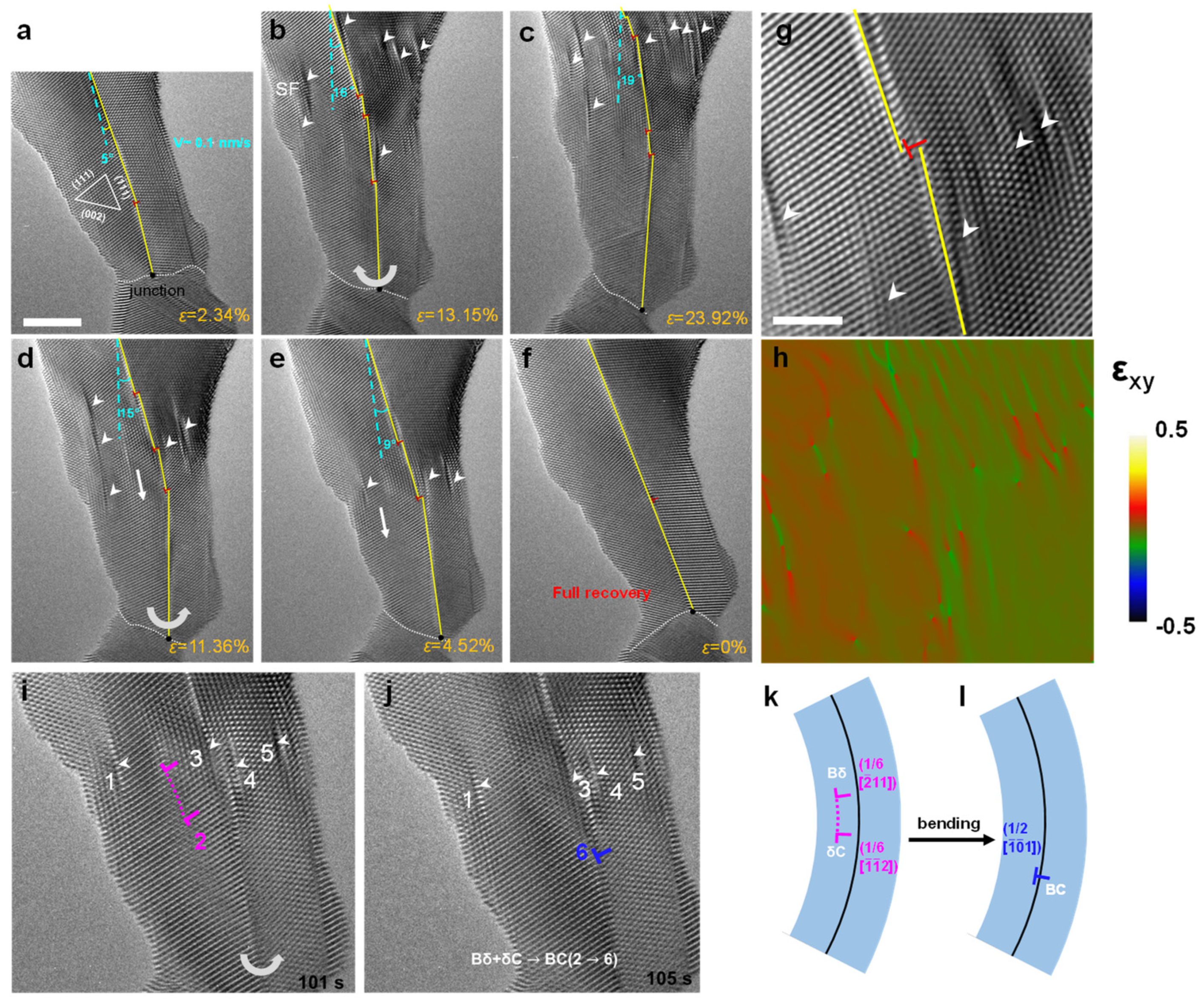
Before the experiments, an Au NW with a longitudinal embedded TB (Figure 1a) was fabricated inside a TEM (see Section 2). The Au NW with a longitudinal TB featured an axial orientation of <110>, with an initial length of ∼25.2 nm and a diameter of ∼10.6 nm. Subsequently, bending tests were conducted on the bottom side of the Au NW by precisely controlling the mobile Au probe at a low loading rate (∼0.7 nm/s). According to classical beam theory, the maximum bending strain (εb) occurring at the left and right surfaces of a bent beam can be calculated as εb = r/(r + R) × 100%, where R represents the radius of curvature of the bent neutral plane and r represents the radius of the NW. Figure 1a–c show a gradual increase in the leftward bending deformation of the Au NW, and the NW finally reached the maximum bending strain of 23.92%. Both the NW and the TB exhibited an increasingly curved shape as the bending strain increased (Figure 1a–c). Frame-by-frame snapshots showed that the bending strain was mainly accommodated by the propagation of SFs nucleated from the free surface and some full dislocations emitted from the TB-GB junction (Figure 1a,b). It is noteworthy that the full dislocations emitted from the junction slipped along the TB, which can be referred to as TB dislocations. The bending strain increased with the successive nucleation of SFs and TB dislocations’ dissociation (Supplementary Figure S2).
Subsequently, reversed bending was imposed and the sample displayed complete recovery of the bending strain (Figure 1d–f). The stress state of the bent nanowire (Figure 1g) was further evaluated using geometric phase analysis (GPA) (GPA has previously been used to measure the displacement field around dislocations to picometer accuracy and strain fields to 0.5% at nanometer-scale spatial resolution [30]) (Figure 1h), which showed that the stress was quite uniform, with no obvious stress concentration over the sample, indicating that the bending strain was well accommodated by the emergence of the TB dislocations and SFs. Intriguingly, enlarged images (Figure 1i,j) showed that the SFs (e.g., SF2 with the burgers vector 1 / 6 2 11   ( B δ )   and   1 / 6 [ 1 1 2 ]   ( δ C ) marked by pink) could slip along ( 1 1 1 ) plane and react with the TB, forming new TB dislocations (e.g., TB dislocation6 with the Burgers vector 1 / 2 1 01   ( BC ) marked in blue) during the bending process. This process greatly released the internal bending strain of NW and promoted subsequent deformation. The newly formed TB dislocations moved downward along the TB in response to the applied stress and ultimately disappeared at the TB-GB interface. During the reverse bending, the recoverable deformation mechanism was primarily dominated by the gliding of SFs along the ( 1 1 1 ) planes and the slipping of TB dislocations along the TB, accompanied by a decrease in the curvature of the nanowires. These dislocations and SFs were finally annihilated at the surface or GBs; then, the TB was transformed into a flat configuration, leading to complete structural recovery (Figure 1f). The schematic diagrams (Figure 1k,l) show the related dislocation reaction during the bending strain recovery process under a low loading rate.
To further understand the atomistic mechanisms of the high recoverable bending strain in experiments, we performed molecular dynamics (MD) simulations of plastic bending in the Au nanowire with a longitudinal TB. We constructed a pillared model similar to the geometry presented in Figure 1a, with a TB embedded in a NW (Figure 2a). Upon bending (Figure 2b,c), some inclined SFs (marked by red arrows) were nucleated and new axial SFs (represented by black arrows) parallel to the TB formed after complete cross-slip (the simplified Thompson tetrahedron to illustrate slip systems and dislocation reactions is shown in Supplementary Figure S3). Dislocation analysis (DXA) in Ovito [29] showed that the corresponding dislocation reaction was (Figure 2d)
B α + α C   BC   B δ + δ C
Moreover, some of the SFs reacted with the TB and induced the generation of TB dislocations ( B α + α′C B δ + δ C ), which was consistent with experimental observations (Figure 1i,j), as schematically shown in Figure 3e. It is noted that, different from the near-perfect right/left surface in the as-constructed MD model (Figure 2a), in our experiment, the SFs were mainly nucleated from the bilateral free surface, which was due to the abundance of steps on the bilateral free surface (Figure 1a–c). Upon reverse bending, the strain in the NW decreased from 14.98% (Figure 2f) to approximately 5.58% (Figure 2h), mediated by SFs’ motion and the complicated dislocation reaction. The SFs in the right grain reacted with the TB to form TB dislocations via a dislocation reaction, and then the TB dislocations again formed SFs in the left grain through cross-slip and dislocation decomposition. The dislocation reaction can be written as
B δ + δ C     B α + α C   B δ + δ C B α + α δ + δ C   B α + α C ,
as shown in Figure 2i. Overall, the simulation results are generally consistent with the experimental observations, despite some differences emerging from the free surface construction.
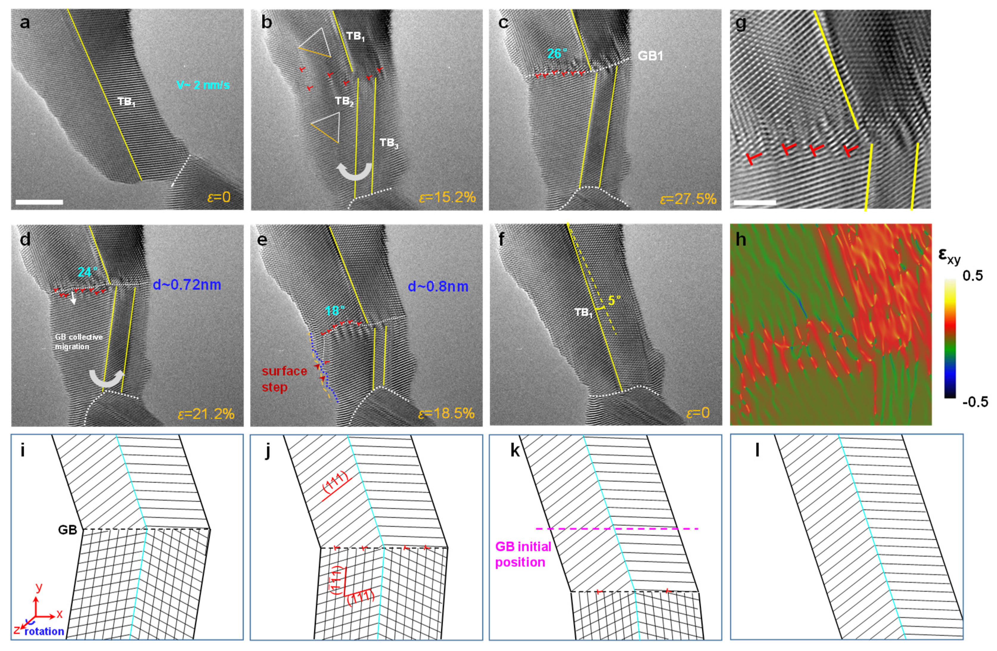
It is well known that loading rates play a crucial role in the deformation characteristics and mechanical behaviors of materials. Here, the loading rate effect was explored by conducting bending cycling on the same sample as in Figure 1, at a higher loading rate of ∼2 nm/s, as shown in Figure 3. Upon loading, some dislocations instantaneously nucleated and climbed into the grain, in response to the rapid stress accumulation in the central region (Figure 3a,b). Due to the high loading rate, more geometrically necessary dislocations (GNDs) were expected to form and arrayed on the center site to accommodate the shape change and relax the energy (Figure 3b). The rapid accumulation of these dislocations led to the formation of dislocation-type high-angle GBs with a tilt angle of ∼26° (GB1). As such, the NW achieved maximum bending strain as high as 27.5% (Figure 3c), surpassing the 7.8% reported in the literature [15]. It should be noted that the loading mode employed in our study was characterized by forward loading followed by reverse loading, as opposed to the conventional load–unload approach. (The aspect ratio, defined as the length to diameter ratio, of the Au nanorods employed in the previous literature (1.77) closely aligns with the aspect ratio of the Au nanorods utilized in the present study (2.38)). Moreover, prior findings have demonstrated that twinned Au nanorods exhibit superior shape recoverability compared to twin-free Au nanorods when subjected to bending deformation. The results demonstrate a significant improvement in the shape recoverability of Au nanorods due to the presence of thin twin sheets, thereby corroborating our hypothesis regarding the pivotal role of TB in facilitating strain recovery. Upon reverse bending, GB dislocations coordinately slipped along the ( 1 1 1 ) planes, resulting in the collective migration of GBs on both sides of the TB (Figure 3d,e). Consequently, excellent bending strain recoverability was accomplished via the cooperative mechanisms of grain rotation and GB migration. It is generally observed that grain rotation is primarily achieved through alterations in the content of GB dislocations [31]. The well-established Frank–Bilby equation suggests that the evolution of GB dislocations leads to changes in the GB misorientation angles between adjacent grains. As the dislocation traverses the lattice, its interaction with the GB results in a modification of the GB misorientation angle. These changes accumulate over time and can lead to substantial changes in GB misorientation angles, a phenomenon referred to as dislocation-induced GB evolution. Specifically, the Frank–Bilby equation can be expressed as [31]: b h = 2 sin θ 2 . Here, b is the edge component of the Burgers vector ( ~ 0.243 nm), and h is the average dislocation spacing. As shown in Figure 3d,e, the averaged dislocation spacing was measured to be 0.72 and 0.8 nm, respectively. Correspondingly, the calculated GB angles were found to be 23.4° and 17.5°, which align well with the measured GB angles of 24° and 18°, respectively. The orange and blue dashed lines in Figure 3e represent outlines sketched to provide visual references. Additionally, the presence of surface steps, marked by red arrows, serves as evidence of dislocations slipping out of the surface.
During the strain recovery process, the misorientation of GB1 gradually decreased since a portion of the SFs slipped out from the surface with reduced bending strain (Figure 3c,d). Finally, this TB became flat again, accompanied by GBs’ collective migration and grain rotation (Figure 3f). Figure 3g,h illustrate the stress distribution of the sample under high loading rates. Therefore, it is hypothesized that the variance in stress distribution is the primary factor behind the structural differences observed under similar bending strain (Figure 1c and Figure 2c). Figure 3i–k provide a schematic representation corresponding to Figure 3d–f, to illustrate the cooperative process involving grain rotation and GB migration. Therefore, irrespective of the low/high loading rate, the plastic deformation caused by the reciprocating bending of Au NWs with a TB can be fully recovered, presenting excellent recoverability. This finding offers valuable insights for the design of flexible electronic materials.
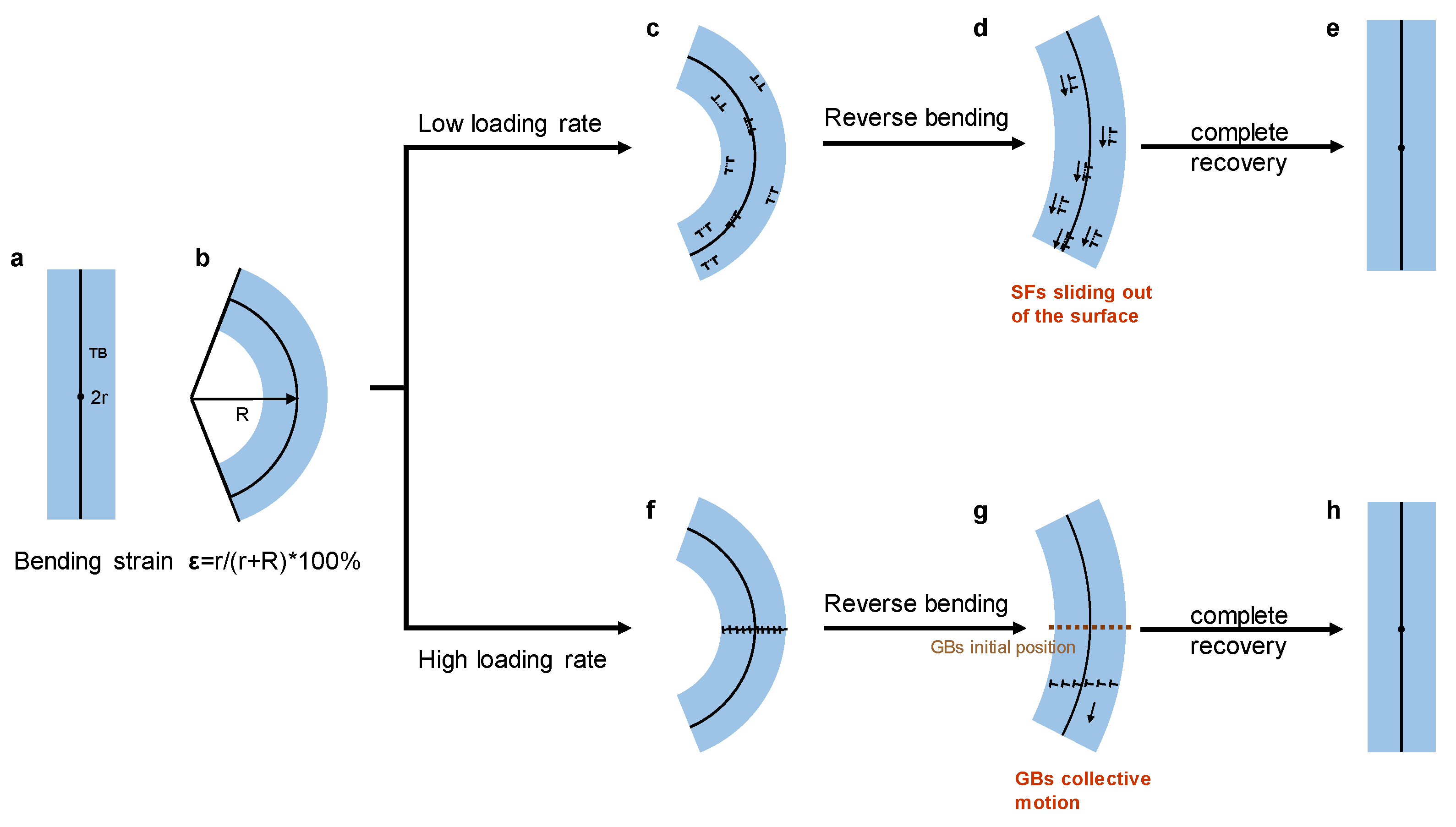
Figure 4 provides the schematic diagrams of the deformation mechanisms of nanowires with axial TBs under different loading rates. In Figure 4a,b, the nanowires length is 2r, and its curvature radius is R after bending deformation. As shown in Figure 4c,d, at low loading rates, some SFs exist inside the nanowire to accommodate the bending strain. As illustrated in Figure 4f,g, the strain gradient caused by high loading rates leads to the formation of GBs to accommodate the shape change and energy relaxation. Finally, with the reverse bending load, the recovery mechanisms were dominated, respectively, by the collective motion of the GBs and the SFs’ slip under high and low loading rates.

4. Discussion

The plastic deformability and recoverability of nanocomponents under bending fatigue loading hold significant importance for their functionality and reliability. Taking advantage of the successful development of in situ bending testing and the controlled preparation of NWs with a longitudinal TB, we discovered the remarkable capability for high bending strain recoverability in NWs through the motion of SF/GB dislocations. Several GB/TB-based approaches have been proposed to improve the recoverability of nanomaterials, including twinning/phase transformation-induced lattice reorientation, the design of gradient lamellar structures, and conservative low-angle GB migration [32]. This exceptional bending strain recoverability is achieved through the simple bending loading of NT NWs, with distinct recovery mechanisms at low and high loading rates. Specifically, at low loading rates, strain recovery is governed by the consecutive slip out of the surface of SFs in the twin/matrix. On the other hand, at high loading rates, the recovery mechanism is dominated by the collective migration of GBs and grain rotation. Moreover, the varying recovery mechanisms observed under different conditions are thought to be attributable to the differing stress distributions that arise from the loading rate.
The influence of various materials on bending deformation is substantial. The previous results showed that, after conducting bending tests on nanowires with FCC metals, Ni nanowires exhibited higher hardness compared to Al and Cu nanowires [33]. This is attributed to the slower slip velocity of dislocations in Ni nanowires compared to other nanowires, requiring larger vertical displacement for fracture. Nevertheless, the exceptional mechanical properties and remarkable chemical inertness of gold nanowires render them a compelling candidate for prospective nanoscale electrical and mechanical devices, and they deserve more attention.
It is worth noting that the remarkable bending strain recovery of the sample is attributed to the involvement of the TB. Specifically, TBs prevail in achieving a strength–ductility synergy as TBs can act as effective sites to store defects. Previous results [25] show that the maximum nominal engineering stress with twinned specimens is approximately 1.6 times that of twin-free specimens with a similar aspect ratio. This is attributed to the presence of TBs, which divide the nanowire into separate regions and pin existing dislocations, impeding further plastic deformation. Here, we found, during the collective migration of GBs, that the TB plays a crucial role as both the starting and ending point for GB slip, facilitating the slip and movement of the GBs, thereby increasing the ductility of the materials. Additionally, the TB-GB junction and TB steps can also act as nucleation sites for dislocations, which contribute to the accumulation and propagation of dislocations and further increase the ductility and work-hardening capability of metallic materials. In our work, this interplay contributed to the achievement of notable recoverable bending strain, reaching approximately 27.5%, as observed in Figure 3. The significant bending strain recoverability demonstrated by NWs with TBs showcases their exceptional ability to accommodate bending plasticity, which provides novel ideas for the design of flexible electronic materials.

5. Conclusions

In summary, the present work elucidates the atomistic mechanisms underlying the deformation of Au NWs with a TB at different loading rates under bending loads. SFs and TB dislocations, nucleated at the free surface and TB-GB interface, are dominant in the NWs. At a low loading rate, SFs are evenly distributed in the twin and matrix. As more dislocations are activated under a high loading rate, this leads to the formation of HAGBs in the middle region of the NW. Surprisingly, the nanowires bend backwards when the bending strain reaches approximately 27.5%, and the strain and structure can almost completely recover without fracture, which has not been seen in previous experiments. However, the dominant recovery mechanism is different in the two cases: at a low loading rate, the mechanism is mainly attributed to the motion of SFs and TB dislocations; at a high loading rate, the collective migration of HAGBs accompanied by grain rotation controls the bending deformation. The experimental results reveal the atomic deformation mechanism under reciprocating bending, which complements the theoretical development of atomic bending deformation mechanisms.

Supplementary Materials

The following supporting information can be downloaded at: https://www.mdpi.com/article/10.3390/cryst13081159/s1, Figure S1: Experimental set-up. Figure S2: Dissociation of TB dislocations upon bending. Figure S3: The simplified Rhompson tetrahedron to illustrate slip systems and dislocation reactions in an fcc lattice.

Author Contributions

Conceptualization, J.W. and H.Z.; methodology, G.C.; software, L.K.; validation, L.K. and G.C.; formal analysis, L.K.; investigation, G.C.; resources, J.W. and H.Z.; data curation, L.K.; writing—original draft preparation, L.K.; writing—review and editing, L.K.; visualization, H.Z.; supervision, J.W.; project administration, J.W.; funding acquisition, J.W. and H.Z. All authors have read and agreed to the published version of the manuscript.

Funding

J.W. acknowledges the support of the Basic Science Center Program for Multiphase Evolution in Hypergravity of the National Natural Science Foundation of China (51988101) and the National Natural Science Foundation of China (52071284). H.Z. acknowledges financial support from the National Natural Science Foundation of China (12222210 and 12172324) and computational support from the National Supercomputer Center in Tianjin and the Beijing Super Cloud Computing Center.

Data Availability Statement

Data generated and supporting the findings of this article are available from the corresponding author upon reasonable request.

Conflicts of Interest

The authors declare no conflict of interest regarding the design, experimentation, simulation, or analysis aspects of the work presented in this manuscript.

References

  1. Wang, Z.L. Towards Self-Powered Nanosystems: From Nanogenerators to Nanopiezotronics. Adv. Funct. Mater. 2008, 18, 3553–3567. [Google Scholar] [CrossRef]
  2. Loh, O.Y.; Espinosa, H.D. Nanoelectromechanical contact switches. Nat. Nanotechnol. 2012, 7, 283–295. [Google Scholar] [CrossRef] [PubMed]
  3. Yu, M.-F.; Lourie, O.; Dyer, M.J.; Moloni, K.; Kelly, T.F.; Ruoff, R.S. Strength and Breaking Mechanism of Multiwalled Carbon Nanotubes Under Tensile Load. Science 2000, 287, 637–640. [Google Scholar] [CrossRef] [Green Version]
  4. Meyers, M.A.; Mishra, A.; Benson, D.J. Mechanical properties of nanocrystalline materials. Prog. Mater. Sci. 2006, 51, 427–556. [Google Scholar] [CrossRef]
  5. Darling, K.A.; Rajagopalan, M.; Komarasamy, M.; Bhatia, M.A.; Hornbuckle, B.C.; Mishra, R.S.; Solanki, K.N. Extreme creep resistance in a microstructurally stable nanocrystalline alloy. Nature 2016, 537, 378–381. [Google Scholar] [CrossRef]
  6. Ke, X.; Ye, J.; Pan, Z.; Geng, J.; Besser, M.F.; Qu, D.; Caro, A.; Marian, J.; Ott, R.T.; Wang, Y.M.; et al. Ideal maximum strengths and defect-induced softening in nanocrystalline-nanotwinned metals. Nat. Mater. 2019, 18, 1207–1214. [Google Scholar] [CrossRef]
  7. Wang, J.; Sansoz, F.; Huang, J.; Liu, Y.; Sun, S.; Zhang, Z.; Mao, S.X. Near-ideal theoretical strength in gold nanowires containing angstrom scale twins. Nat. Commun. 2013, 4, 1742. [Google Scholar] [CrossRef] [Green Version]
  8. Wu, B.; Heidelberg, A.; Boland, J.J. Mechanical properties of ultrahigh-strength gold nanowires. Nat. Mater. 2005, 4, 525–529. [Google Scholar] [CrossRef]
  9. Cheng, G.; Yin, S.; Chang, T.H.; Richter, G.; Gao, H.; Zhu, Y. Anomalous Tensile Detwinning in Twinned Nanowires. Phys. Rev. Lett. 2017, 119, 256101. [Google Scholar] [CrossRef] [Green Version]
  10. Liu, L.; Deng, Q.; Su, M.; An, M.; Wang, R. Strain rate and temperature effects on tensile behavior of Ti/Al multilayered nanowire: A molecular dynamics study. Superlattices Microstruct. 2019, 135, 106272. [Google Scholar] [CrossRef]
  11. Xu, W.; Kim, W.K. Molecular dynamics simulation of the uniaxial tensile test of silicon nanowires using the MEAM potential. Mech. Mater. 2019, 137, 103140. [Google Scholar] [CrossRef]
  12. Yue, Y.; Zhang, Q.; Zhang, X.; Yang, Z.; Yin, P.; Guo, L. In Situ Observation of Twin Boundary Sliding in Single Crystalline Cu Nanowires. Small 2017, 13, 1604296. [Google Scholar] [CrossRef] [PubMed]
  13. Zhang, X.; Li, X.; Gao, H. Size and strain rate effects in tensile strength of penta-twinned Ag nanowires. Acta Mech. Sin. 2017, 33, 792–800. [Google Scholar] [CrossRef]
  14. Liu, H.; Zhou, J. Plasticity in nanotwinned polycrystalline Ni nanowires under uniaxial compression. Mater. Lett. 2016, 163, 179–182. [Google Scholar] [CrossRef]
  15. He, S.; Jiang, B.; Wang, C.; Chen, C.; Duan, H.; Jin, S.; Ye, H.; Lu, L.; Du, K. High Reversible Strain in Nanotwinned Metals. ACS Appl. Mater. Interfaces 2021, 13, 46088–46096. [Google Scholar] [CrossRef] [PubMed]
  16. Wu, H.; Kong, D.; Ruan, Z.; Hsu, P.C.; Wang, S.; Yu, Z.; Carney, T.J.; Hu, L.; Fan, S.; Cui, Y. A transparent electrode based on a metal nanotrough network. Nat. Nanotechnol. 2013, 8, 421–425. [Google Scholar] [CrossRef]
  17. Takei, K.; Takahashi, T.; Ho, J.C.; Ko, H.; Gillies, A.G.; Leu, P.W.; Fearing, R.S.; Javey, A. Nanowire active-matrix circuitry for low-voltage macroscale artificial skin. Nat. Mater. 2010, 9, 821–826. [Google Scholar] [CrossRef]
  18. Huang, Q.; Yu, D.; Xu, B.; Hu, W.; Ma, Y.; Wang, Y.; Zhao, Z.; Wen, B.; He, J.; Liu, Z.; et al. Nanotwinned diamond with unprecedented hardness and stability. Nature 2014, 510, 250–253. [Google Scholar] [CrossRef]
  19. Pan, Q.; Zhou, H.; Lu, Q.; Gao, H.; Lu, L. History-independent cyclic response of nanotwinned metals. Nature 2017, 551, 214–217. [Google Scholar] [CrossRef]
  20. Lu, L.; Shen, Y.; Chen, X.; Qian, L.; Lu, K. Ultrahigh strength and high electrical conductivity in copper. Science 2004, 304, 422–426. [Google Scholar] [CrossRef] [Green Version]
  21. Lu, Q.; You, Z.; Huang, X.; Hansen, N.; Lu, L. Dependence of dislocation structure on orientation and slip systems in highly oriented nanotwinned Cu. Acta Mater. 2017, 127, 85–97. [Google Scholar] [CrossRef]
  22. Lu, K. Stabilizing nanostructures in metals using grain and twin boundary architectures. Nat. Rev. Mater. 2016, 1, 16019. [Google Scholar] [CrossRef]
  23. Lu, L.; Zhu, T.; Shen, Y.; Dao, M.; Lu, K.; Suresh, S. Stress relaxation and the structure size-dependence of plastic deformation in nanotwinned copper. Acta Mater. 2009, 57, 5165–5173. [Google Scholar] [CrossRef]
  24. Lu, N.; Du, K.; Lu, L.; Ye, H.Q. Transition of dislocation nucleation induced by local stress concentration in nanotwinned copper. Nat. Commun. 2015, 6, 7648. [Google Scholar] [CrossRef] [PubMed] [Green Version]
  25. Zhu, W.; Wang, H.; Yang, W. Orientation- and microstructure-dependent deformation in metal nanowires under bending. Acta Mater. 2012, 60, 7112–7122. [Google Scholar] [CrossRef]
  26. Zhan, H.F.; Gu, Y.T. Theoretical and numerical investigation of bending properties of Cu nanowires. Comput. Mater. Sci. 2012, 55, 73–80. [Google Scholar] [CrossRef] [Green Version]
  27. Stukowski, A. Visualization and analysis of atomistic simulation data with OVITO–the Open Visualization Tool. Model. Simul. Mater. Sci. Eng. 2010, 18, 015012. [Google Scholar] [CrossRef]
  28. Wang, L.; Teng, J.; Liu, P.; Hirata, A.; Ma, E.; Zhang, Z.; Chen, M.; Han, X. Grain rotation mediated by grain boundary dislocations in nanocrystalline platinum. Nat. Commun. 2014, 5, 4402. [Google Scholar] [CrossRef] [Green Version]
  29. Zhu, Q.; Huang, Q.; Guang, C.; An, X.; Mao, S.X.; Yang, W.; Zhang, Z.; Gao, H.; Zhou, H.; Wang, J. Metallic nanocrystals with low angle grain boundary for controllable plastic reversibility. Nat. Commun. 2020, 11, 3100. [Google Scholar] [CrossRef]
  30. Hӱtch, M.J.; Snoeck, E.; Kilaas, R. Quantitative measurement of displacement and strain fields from HREM micrographs. Ultramicroscopy 1998, 74, 131–146. [Google Scholar] [CrossRef]
  31. Plimpton, S. Fast Parallel Algorithms for Short-Range Molecular Dynamics. J. Comput. Phys. 1995, 117, 1–19. [Google Scholar] [CrossRef] [Green Version]
  32. Grochola, G.; Russo, S.P.; Snook, I.K. On fitting a gold embedded atom method potential using the force matching method. J. Chem. Phys. 2005, 123, 204719. [Google Scholar] [CrossRef] [PubMed]
  33. Deb Nath, S.K. Elastic, elastic–plastic properties of Ag, Cu and Ni nanowires by the bending test using molecular dynamics simulations. Comput. Mater. Sci. 2014, 87, 138–144. [Google Scholar] [CrossRef]
Figure 1. Recoverable strain of Au nanowire at low loading rate. (ac) High-resolution transmission electron microscope (HRTEM) snapshots showing the bending process of an Au NW embedded with a TB. With increasing strain, more SFs were nucleated and emitted from the free surface (indicated by the white arrows). Some of the TB dislocations emitted from the TB-GB junction, forming TB dislocations and gliding along the TB. The yellow line and white dotted line indicate the TB and the GB produced by the contact of the probe side and static side, respectively. (df) Atomic-scale images of the reverse-bending Au nanowire. Upon bending, SFs migrated downward, accompanied by a reduction in bending strain. The sample could be completely recovered without defects. (g,h) The HRTEM image (a frame during b,c) and corresponding shear strain map from geometric phase analysis (GPA). The shear strain map (εxy) and the color variation from black to yellow indicate the variation in shear strain values from −0.5 to 0.5. (i,j) Dislocation reaction of formation of TB dislocation during the strain recovery process. (k,l) The corresponding diagram of (i,j). Scale bar: 5 nm.
Crystals 13 01159 g001
Figure 2. Bending-induced dynamic evolution of nanowires with TBs. (ac) Dislocation reactions during bending. (d) Some of the inclined SFs cross-slip to form axial SFs, and (e) the remaining ones react with TB to form TB dislocations (e). (fh) Upon reverse bending, most defects slip out of the surface, accompanied by high strain recovery. (i) The related dislocation reaction during the reverse bending. The axial SFs (Bδ and δC) cross-slip to form inclined SFs (Bα and αC). The newly formed SFs (Bα and αC) react with TB to form TB dislocations (Bδ and δC) via dislocation reaction, and then TB dislocations again form SFs (Bα′ and α′C) in the left grain through cross-slip and dislocation decomposition.
Crystals 13 01159 g002
Figure 3. In situ TEM images show the high recoverable strain mediated by GB migration, which mediated the recoverable bending of the nanowires with a TB under a high loading rate. (ac) HRTEM images showing the GB formation process resulting from the regular arrangement of GB dislocations to accommodate the bending strain. (df) With the loading of reverse bending, the GB misorientation gradually decreases from 24° to 0°, accompanied by the defects that slipped out of the surface (evidenced by the surface steps marked by red arrows) or slipped to the TB-GB interface. (g,h) The HRTEM image (a frame in the b,c process) and corresponding shear strain distribution from GPA. (il) The schematic diagrams of the deformation mechanisms of high recoverable bending strain under high loading rate. Scale bar: 5 nm.
Crystals 13 01159 g003
Figure 4. The schematic diagrams of the deformation mechanism under different loading rates. (a) A nanowire with an axial TB, and the nanowires length is 2r. (b) After bending, its nanowire’s radius is R. At a low loading rate (ce), the bending-induced SFs are uniformly distributed throughout the entire sample. Under reverse loading, the deformation mechanism is dominated by SFs’ motion. At a high loading rate (fh), new GBs are formed because more dislocations are activated and aligned at the center of the nanowires. The strain recovery mechanism is mainly dominated by the reversible migration of GBs.
Crystals 13 01159 g004
Disclaimer/Publisher’s Note: The statements, opinions and data contained in all publications are solely those of the individual author(s) and contributor(s) and not of MDPI and/or the editor(s). MDPI and/or the editor(s) disclaim responsibility for any injury to people or property resulting from any ideas, methods, instructions or products referred to in the content.

