Communication

First-Principle Study of Two-Dimensional SiP2 for Photocatalytic Water Splitting with Ultrahigh Carrier Mobility

1
School of Automotive & Transportation Engineering, Shenzhen Polytechnic, Shenzhen 518055, China
2
School of Information Science and Technology, Nanjing Forestry University, Nanjing 210037, China
3
School of Mechanical Engineering, Southeast University, Nanjing 211189, China
4
School of Mechanical and Electronic Engineering, Nanjing Forestry University, Nanjing 210037, China
*
Authors to whom correspondence should be addressed.
Crystals 2023, 13(6), 981; https://doi.org/10.3390/cryst13060981
Submission received: 2 June 2023 / Revised: 14 June 2023 / Accepted: 15 June 2023 / Published: 20 June 2023
(This article belongs to the Special Issue Semiconductor Photocatalysts)

Abstract

:
Two-dimensional materials present abundant novel properties when used in advanced applications, which develops considerable focus. In this investigation, the first-principles calculations are explored to study the structural characteristic of the monolayered SiP2, which is stable even at 1200 K. The SiP2 monolayer is a semiconductor with an indirect bandgap of 2.277 eV. The decent band alignment and light absorption capacity imply that the application is a suitable photocatalyst for water splitting. Furthermore, the SiP2 monolayer possesses an ultrafast electron mobility at 33,153 cm2·V−1·s−1 in the transport direction. The excellent Gibbs free energy of the SiP2 monolayer is also addressed in an examination of the hydrogen evolution reaction.

1. Introduction

With the discovery of graphene in 2004 [1], two-dimensional (2D) materials gradually have gained considerable research, such as magnetic [2], thermal [3,4] and catalytic performances [5]. Two-dimensional materials have robust chemical bonds in the two-dimensional plane, which can even be prepared from corresponding bulk materials by way of mechanical stripping method [6]. Importantly, 2D materials exhibit excellent mechanical [7], magnetic [8] and optical properties [9]. For example, under external biaxial strain, the bandgap of the arsenene can be transformed from indirect to direct bandgap. Furthermore, as the strain continues to increase, the optical absorption ability of arsenene also can be enhanced, enabling optical absorption energy that ranges in 1.2–2.2 eV [10]. The hardness of GeC is weaker than that of graphene, while the obtained Poisson value (about 0.28) is 1.5 times that of graphene. At the same time, the in-plane stiffness of the GeC is 41%, and the GeC possesses a small limited strain under biaxial strain [11]. All of this reveals the promising applications used by 2D materials [12,13,14,15]. To further develop the advanced functional 2D materials and potential applications, some significant methods are adopted. Contacting two different layered materials as type-II van der Waals can separate photogenerated electrons and holes, which prolongs the lifetime of the charges when used as a photocatalyst for water splitting [16,17,18,19]. The hydrogen evolution reaction (HER) ability of the MoS2 monolayer in the inert basal planes can be activated by using different intrinsic defects [20]. Furthermore, external strain and electric field engineering are also advantageous for improving the catalytic, electronic and thermal performances [21,22,23].
Since Fujishima and Honda first reported that TiO2 electrodes can be collectively used as a photocatalyst for water splitting in 1972 [24], developing 2D materials to decompose the water became desirable. When the 2D semiconductor absorbs the photons from the light, the excited electrons can migrate from the valence band (VB) to the conduction band (CB) to induce the HER and oxygen evolution reaction (OER), respectively. For example, the stripped g-C3N4 nanosheets can greatly increase the efficiency of its photocatalytic water decomposition by increasing the specific surface area in order to increase the activity [25]. Carrier mobility of the photogenerated electrons and holes is also a critical parameter in water splitting [26], because the higher mobilities can obtain a high utilization of electrons and holes in oxidations and reductions before recombination. A recent study on photocatalytic water splitting reported that the GeSe monolayer even possesses ultrahigh electron mobility at about 32,507 cm2·V−1·s−1 [27]. Recently, 2D SiP2 has been successfully prepared [28], which presents in an unconventional excitonic state. Subsequently, SiP2 also can be prepared with h-BN used as a gate-controlled phototransistor, which additionally demonstrates an ultrahigh sensitivit. All of this demonstrates that SiP2 has excellent electronic and optical properties. Current investigations have revealed a promising application for nanodevices, while the critical parameter of carrier mobility has been rarely explored. Furthermore, the suitable band edge energy of the SiP2 monolayer has also not been studied, even though it may have a potential application as a photocatalyst. All these things have aroused the exploration of the advanced applications of the SiP2 monolayer in our work.
In this investigation, the thermal stability and electronic property of the SiP2 monolayer are addressed by the first-principles method. The semiconductor nature is obtained and the band edge positions are also explored as suitable for redox reaction in water splitting. Additionally, the excellent carrier mobility and the hydrogen evolution reaction performance are first examined for the promising novel photocatalytic activity of the SiP2 monolayer. The research outline of this investigation is expressed by Figure 1.

2. Computational Methods

In our simulations, the structural optimization, phonon spectrum, band structure, carrier mobility and the Gibbs free energy were calculated by Device Studio [Hongzhiwei Technology, Device Studio, Version 2021A, China, 2021. Available online: https://iresearch.net.cn/cloudSoftware, accessed on 2 June 2023] program, which provides a number of functions for performing visualization, modeling and simulation. And all that simulations using DS-PAW software are integrated in Device Studio program [29]. Based on density functional theory (DFT), the Vienna ab initio simulation package (VASP) was explored to develop the other first-principles calculations [30]. The generalized gradient approximation (GGA) method was used with the projector augmented wave potentials (PAW) to employ the Perdew–Burke–Ernzerhof (PBE) functional, which also explains the exchange-correlation functional [31,32]. The energy cut-off used was 550 eV. In the first Brillouin zone (BZ), the Monkhorst–Pack k-point grid was set to 17 × 17 × 1. In addition, the Heyd–Scuseria–Ernzerhof hybrid method was adopted to calculated the projected band structure [33]. The vacuum space was set at 25 Å, which can prevent the interaction between nearby layers. The convergence for the energy is 0.01 meV, while the force is controlled at 0.01 eV·Å−1. The PHONOPY code was used to calculated phonon spectra based on the density functional perturbation theory [34,35].

3. Results and Discussion

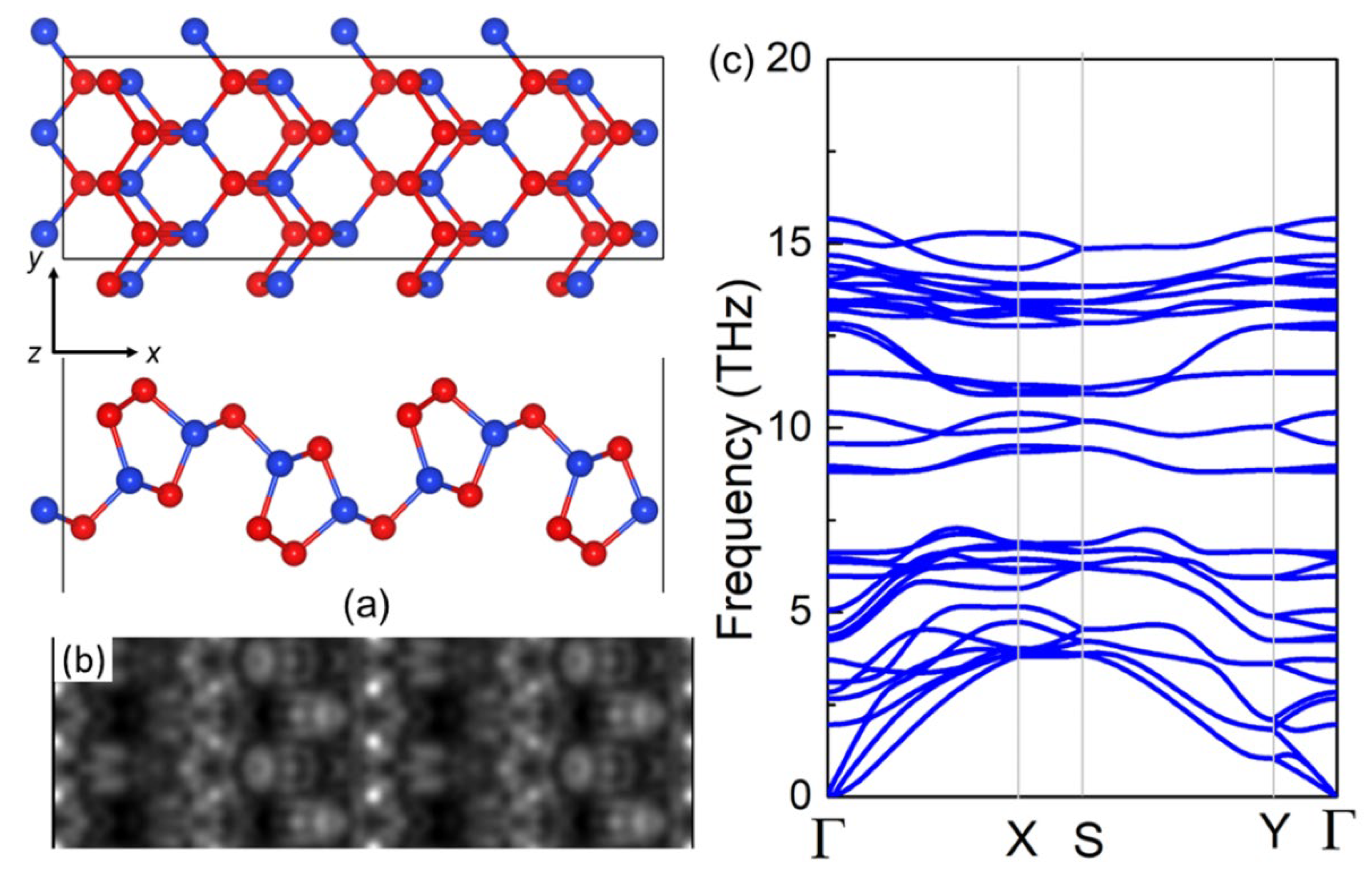
3.1. Structural and Stability Performance

The atomic structure of the SiP2 monolayer was optimized with the lattice constant at 3.460 Å and 10.280 Å in the x and y directions, respectively, as is demonstrated in Figure 2a. The lattice constant of 3.460 Å is comparable with that of the TMDs materials [36] and the B2P6 monolayer (about 3.25 Å) [37], showing a promising application as a stable heterostructure. The simulated scanning tunneling microscopy (STM) images of the SiP2 monolayer obtained are shown in Figure 2b, and such patterns in the simulated STM images display good agreement with a previous experiment [28]. Moreover, the dynamic stability of the SiP2 monolayer was investigated by using the density functional perturbation theory as shown in Figure 2c; one can see that no imagery was found in phonon spectra, suggesting dynamic stability of the SiP2 monolayer.
Then, the thermal stability of the SiP2 monolayer under different temperatures was further investigated. Using ab initio molecular dynamics (AIMD) calculations, the Nosé–Hoover heat bath scheme was addressed to further evaluate the thermal stability of the SiP2 monolayer. A 4 × 2 × 1 supercell of the SiP2 was employed, considering the lattice translational constraints, which possesses 36 atoms in the simulations. After the total relaxation under 300–1200 K in 10 ps, the structure of the SiP2 system was still intact, demonstrated by the inset image in Figure 2a. Such results represent a robust thermal stability of the SiP2 monolayer even under 1200 K. In addition, a convergence was revealed by the fluctuations in temperature and total energy of the SiP2 monolayer during the AIMD calculation under 300–1200 K as shown in Figure 3, further suggesting the accuracy of the obtained results.

3.2. Band Structure and Carrier Mobility

The projected band structure of the SiP2 monolayer was calculated using the HSE06 functional expressed in Figure 4a. One can see that the SiP2 monolayer is a semiconductor with an indirect bandgap of 2.277 eV, which displays good agreement with other reported results [28]. The conduction band minimum of the SiP2 monolayer is mainly contributed to by the P atoms, while the valence band maximum is donated to by the P and Si atoms, as is demonstrated in Figure 4a. By comparing the vacuum level, the band edge positions of the SiP2 monolayer were calculated, as is shown in Figure 4b. The obtained band alignment of the SiP2 monolayer suggests a suitable band energy to promote the oxidations and reductions in water splitting; such decent band energy was also addressed by the WS2 monolayer in some TMDs materials insinuated in Figure 4b. Furthermore, the light absorption capacity of the SiP2 monolayer was investigated as a photocatalyst. The anisotropy optical performance of the SiP2 monolayer is shown in Figure 4c, with the peak of the light absorption spectrum along the x (or y) direction as 12.8 × 105 cm−1 (or 10.2 × 105 cm−1) and with the wavelength as 207 nm (or 155 nm), which is higher than that of B2P6 (3.4 × 104 cm−1) [37], CdO (3.56 × 105 cm−1) [38] arsenene (3.01 × 105 cm−1) [39]. Such excellent light absorption characteristics also demonstrate the potential use as a photocatalyst to decompose water.
The carrier mobility of the SiP2 monolayer is calculated by using the Bardeen–Shockley deformation potential theory [40], because the carrier mobility is also a critical target in photocatalytic water splitting. The effective masses (m*) of the electron and hole are obtained by:
m * = ± 2 d 2 E k   d k 2 1 ,
where k and Ek are the wave vector and the corresponding electronic energy, respectively. In addition, the carrier mobility (μ) of the SiP2 monolayer is calculated from:
μ = e 3 C k B T m * m e E d 2 ,
where the temperature, the electron charge and the Planck constant are expressed by T, e and , respectively. The Boltzmann constant is represented by kB. The change of the band edge energy of the SiP2 monolayer was evaluated by the deformation potential (Ed), which is calculated by comparing the vacuum level. In addition, the elastic modulus is used by C, which is calculated using C = 2 E / ε 2 / S . The total energy of the SiP2 monolayer is E and the area of the system is S. The energy difference and the band edge energy under the external strain of the SiP2 monolayer were obtained, as is shown in Figure 5, and the fitted elastic modulus are summarized in Table 1.
The calculated hole carrier of the SiP2 monolayer was 1926 cm2·V−1·s−1 and 3915 cm2·V−1·s−1 along the x and y directions, respectively. Particularly, the electron carrier presented ultrafast mobility at 14,254 cm2·V−1·s−1 and 33,153 cm2·V−1·s−1, respectively. Such excellent mobility was even higher than black phosphorus (10,000 cm2·V−1·s−1) [41] and Li2B6 (6800 cm2·V−1·s−1) [42]. The obtained hole carrier of the SiP2 monolayer was also higher than that of recently reported 2D materials, such as GeS (1312 cm2·V−1·s−1) [27] and HfSi2N4 (1182 cm2·V−1·s−1) [7]. Furthermore, one can see that the mobility of the electron was about 10 times higher than that of the hole, suggesting a more advantageous ability to separate electron and hole in water splitting [43].

3.3. Hydrogen Evolution Reaction Performance

As a photocatalyst, the catalytic ability of the SiP2 monolayer also played a significant role. The Gibbs free energy (∆GH*) of the intermediate product in hydrogen evolution reaction (HER) is calculated by standard conditions from:
ΔGH* = ΔE + ΔEzpe + TΔS,
where the ΔE is used to represent the total energy of the H-adsorbed SiP2 monolayer system, as shown in Figure 6a; the representative highly symmetrical adsorption sites are expressed by yellow balls, which contain 24 possibilities. The ΔEzpe is the difference in the zero-point energies, and the ΔS shows the change in the entropy under the adsorption. T is set at 298 K. The active site is highlighted by the “*”. In addition, the hydrogen evolution reaction characteristic is addressed by two reactions:
∗ + H+ + e → H,
H + H+ + e → H2 + ∗
Furthermore, the most favorable hydrogen evolution reaction by the H-adsorbed site on the SiP2 system is illustrated in Figure 6a as cyan balls, and the obtained Gibbs free energy of such an H-adsorbed SiP2 system was calculated by using 1.11 eV, as shown in Figure 5b. Obviously, the SiP2 monolayer possesses a novel and more advantageous hydrogen evolution reaction than the graphene [44], MoGe2N4 [7] and IV–VI monolayers [27].

4. Conclusions

In this study, the first-principles calculations were explored to systematically investigate the structural, electronic and optical properties and the carrier mobility and hydrogen evolution reaction of the SiP2 monolayer. The SiP2 monolayer is a semiconductor, which has a thermal stability even at 1200 K. The decent band edge positions and optical properties are addressed. Furthermore, the SiP2 monolayer shows anisotropic carrier transport properties with ultrafast electron mobility at 33,153 cm2·V−1·s−1. The excellent hydrogen evolution reaction of the SiP2 monolayer was calculated, which is more advantageous than that of graphene. All these things demonstrate the potential application for using SiP2 as a photocatalyst to decompose water.

Author Contributions

Conceptualization, R.Z.; methodology, H.S.; software, J.L.; validation, H.S.; formal analysis, J.L.; investigation, J.L.; resources, H.P., original draft preparation, J.L. and K.R. All authors have read and agreed to the published version of the manuscript.

Funding

We thank the Shenzhen Polytechnic Research Fund (6023310003k) and the Natural Science Foundation of Jiangsu (BK20220407).

Data Availability Statement

The data presented in this study are available upon request from the corresponding author.

Acknowledgments

We gratefully acknowledge HZWTECH for providing computation facilities. We thank Jie Li from HZWTECH for help and discussions regarding this study.

Conflicts of Interest

The authors declare no conflict of interest.

References

  1. Geim, A.K.; Novoselov, K.S. The rise of graphene. Nat. Mater. 2007, 6, 183–191. [Google Scholar] [CrossRef]
  2. Hou, Y.; Wei, Y.; Yang, D.; Wang, K.; Ren, K.; Zhang, G. Enhancing the Curie Temperature in Cr2Ge2Te6 via Charge Doping: A First-Principles Study. Molecules 2023, 28, 3893. [Google Scholar] [CrossRef]
  3. Qin, H.; Zhang, G.; Ren, K.; Pei, Q.-X. Thermal Conductivities of PtX2 (X = S, Se, and Te) Monolayers: A Comprehensive Molecular Dynamics Study. J. Phys. Chem. C 2023, 127, 8411–8417. [Google Scholar] [CrossRef]
  4. Cui, Q.; Ren, K.; Zheng, R.; Zhang, Q.; Yu, L.; Li, J. Tunable thermal properties of the biphenylene and the lateral heterostructure formed with graphene: A molecular dynamics investigation. Front. Phys. 2022, 10, 1085367. [Google Scholar] [CrossRef]
  5. Ye, H.; Ren, K.; Wang, P.; Wang, L. The investigation of the NH3-SCR performance of a copper-based AEI-CHA intergrown zeolite catalyst. Front. Chem. 2022, 10, 1069824. [Google Scholar] [CrossRef]
  6. Di Bartolomeo, A. Emerging 2D Materials and Their Van Der Waals Heterostructures. Nanomaterials 2020, 10, 579. [Google Scholar] [CrossRef] [Green Version]
  7. Ren, K.; Shu, H.; Wang, K.; Qin, H. Two-dimensional MX2Y4 systems: Ultrahigh carrier transport and excellent hydrogen evolution reaction performances. Phys. Chem. Chem. Phys. 2023, 25, 4519–4527. [Google Scholar] [CrossRef]
  8. Wang, K.; Ren, K.; Hou, Y.; Cheng, Y.; Zhang, G. Physical insights into enhancing magnetic stability of 2D magnets. J. Appl. Phys. 2023, 133, 110902. [Google Scholar] [CrossRef]
  9. Ren, K.; Ma, X.; Liu, X.; Xu, Y.; Huo, W.; Li, W.; Zhang, G. Prediction of 2D IV–VI semiconductors: Auxetic materials with direct bandgap and strong optical absorption. Nanoscale 2022, 14, 8463–8473. [Google Scholar] [CrossRef]
  10. Shu, H.; Niu, Y.X.; Guo, J. Electronic structures and optical properties of arsenene and antimonene under strain and an electric field. J. Mater. Chem. 2018, 6, 83–90. [Google Scholar] [CrossRef]
  11. Peng, Q.; Chao, L.; Wei, J.; De, S. A first-principles study of the mechanical properties of g-GeC. Mech. Mater. 2013, 64, 135–141. [Google Scholar] [CrossRef]
  12. He, J.; Ding, G.; Zhong, C.; Li, S.; Li, D.; Zhang, G. Remarkably enhanced ferromagnetism in a super-exchange governed Cr2Ge2Te6 monolayer via molecular adsorption. J. Mater. Chem. C 2019, 7, 5084–5093. [Google Scholar] [CrossRef]
  13. He, J.; Ding, G.; Zhong, C.; Li, S.; Li, D.; Zhang, G. Cr2TiC2-based double MXenes: Novel 2D bipolar antiferromagnetic semiconductor with gate-controllable spin orientation toward antiferromagnetic spintronics. Nanoscale 2018, 11, 356–364. [Google Scholar] [CrossRef] [PubMed]
  14. Chen, M.; Li, J.; Zhang, J.; Ma, Y.; Dong, H.; Li, W.; Bekyarova, E.; Al-Hadeethi, Y.F.; Chen, L.; Hedhili, M.N.; et al. Evolution of cellulose acetate to monolayer graphene. Carbon 2021, 174, 24–35. [Google Scholar] [CrossRef]
  15. Xue, F.; Zhang, C.; Ma, Y.; Wen, Y.; He, X.; Yu, B.; Zhang, X. Integrated Memory Devices Based on 2D Materials. Adv. Mater. 2022, 34, 2201880. [Google Scholar] [CrossRef] [PubMed]
  16. Wang, G.; Zhi, Y.; Bo, M.; Xiao, S.; Li, Y.; Zhao, W.; Li, Y.; Li, Y.; He, Z. 2D Hexagonal Boron Nitride/Cadmium Sulfide Heterostructure as a Promising Water-Splitting Photocatalyst. Phys. Status Solidi 2019, 257, 1900431. [Google Scholar] [CrossRef]
  17. Wang, G.-Z.; Zhang, L.; Li, Y.; Zhao, W.; Kuang, A.; Li, Y.; Xia, L.; Li, Y.; Xiao, S. Biaxial strain tunable photocatalytic properties of 2D ZnO/GeC heterostructure. J. Phys. D Appl. Phys. 2020, 53, 015104. [Google Scholar] [CrossRef]
  18. Wang, G.; Li, Z.; Wu, W.; Guo, H.; Chen, C.; Yuan, H.; Yang, S.A. A two-dimensional h-BN/C2N heterostructure as a promising metal-free photocatalyst for overall water-splitting. Phys. Chem. Chem. Phys. 2020, 22, 24446–24454. [Google Scholar] [CrossRef]
  19. Wang, G.; Gong, L.; Li, Z.; Wang, B.; Zhang, W.; Yuan, B.; Zhou, T.; Long, X.; Kuang, A. A two-dimensional CdO/CdS heterostructure used for visible light photocatalysis. Phys. Chem. Chem. Phys. 2020, 22, 9587–9592. [Google Scholar] [CrossRef]
  20. Ouyang, Y.; Ling, C.; Chen, Q.; Wang, Z.; Shi, L.; Wang, J. Activating Inert Basal Planes of MoS2 for Hydrogen Evolution Reaction through the Formation of Different Intrinsic Defects. Chem. Mater. 2016, 28, 4390–4396. [Google Scholar] [CrossRef]
  21. Conley, H.J.; Wang, B.; Ziegler, J.I.; Haglund, R.F., Jr.; Pantelides, S.T.; Bolotin, K.I. Bandgap Engineering of Strained Monolayer and Bilayer MoS2. Nano Lett. 2013, 13, 3626–3630. [Google Scholar] [CrossRef] [PubMed] [Green Version]
  22. Sun, M.; Chou, J.-P.; Ren, Q.; Zhao, Y.; Yu, J.; Tang, W. Tunable Schottky barrier in van der Waals heterostructures of graphene and g-GaN. Appl. Phys. Lett. 2017, 110, 173105. [Google Scholar] [CrossRef]
  23. Liu, X.; Zhang, G.; Zhang, Y.-W. Topological Defects at the Graphene/h-BN interface Abnormally Enhance Its Thermal Conductance. Nano Lett. 2016, 16, 4954–4959. [Google Scholar] [CrossRef]
  24. Fujishima, A.; Honda, K. Electrochemical photocatalysis of water at semiconductor electrode. Nature 1972, 238, 5358. [Google Scholar] [CrossRef]
  25. Tan, C.; Cao, X.; Wu, X.-J.; He, Q.; Yang, J.; Zhang, X.; Chen, J.; Zhao, W.; Han, S.; Nam, G.-H.; et al. Recent Advances in Ultrathin Two-Dimensional Nanomaterials. Chem. Rev. 2017, 117, 6225–6331. [Google Scholar] [CrossRef] [PubMed]
  26. Ren, K.; Wang, S.; Luo, Y.; Chou, J.-P.; Yu, J.; Tang, W.; Sun, M. High-efficiency photocatalyst for water splitting: A Janus MoSSe/XN (X = Ga, Al) van der Waals heterostructure. J. Phys. Phys. D. Appl. Phys. 2020, 53, 185504. [Google Scholar] [CrossRef]
  27. Huang, Z.; Ren, K.; Zheng, R.; Wang, L.; Wang, L. Ultrahigh Carrier Mobility in Two-Dimensional IV–VI Semiconductors for Photocatalytic Water Splitting. Molecules 2023, 28, 4126. [Google Scholar] [CrossRef]
  28. Zhou, L.; Huang, J.; Windgaetter, L.; Ong, C.S.; Zhao, X.; Zhang, C.; Tang, M.; Li, Z.; Qiu, C.; Latini, S.; et al. Unconventional excitonic states with phonon sidebands in layered silicon diphosphide. Nat. Mater. 2022, 21, 773–778. [Google Scholar] [CrossRef]
  29. Blöchl, P.E. Projector augmented-wave method. Phys. Rev. B 1994, 50, 17953. [Google Scholar] [CrossRef] [Green Version]
  30. Capelle, K. A bird’s-eye view of density-functional theory. Braz. J. Phys. 2006, 36, 1318–1343. [Google Scholar] [CrossRef] [Green Version]
  31. Kresse, G.; Joubert, D. From ultrasoft pseudopotentials to the projector augmented-wave method. Phys. Rev. B 1999, 59, 1758–1775. [Google Scholar] [CrossRef]
  32. Perdew, J.P.; Burke, K.; Ernzerhof, M. Generalized gradient approximation made simple. Phys. Rev. Lett. 1996, 77, 3865–3868. [Google Scholar] [CrossRef] [PubMed] [Green Version]
  33. Heyd, J.; Peralta, J.; Scuseria, G.E.; Martin, R.L. Energy band gaps and lattice parameters evaluated with the Heyd-Scuseria-Ernzerhof screened hybrid functional. J. Chem. Phys. 2005, 123, 174101. [Google Scholar] [CrossRef]
  34. Togo, A.; Tanaka, I. First principles phonon calculations in materials science. Scr. Mater. 2015, 108, 1–5. [Google Scholar] [CrossRef] [Green Version]
  35. Togo, A.; Oba, F.; Tanaka, I.J.P.R.B. First-principles calculations of the ferroelastic transition between rutile-type and CaCl2-type SiO2 at high pressures. Phys. Rev. B 2008, 78, 134106. [Google Scholar] [CrossRef] [Green Version]
  36. Zhuang, H.L.; Hennig, R.G. Computational Search for Single-Layer Transition-Metal Dichalcogenide Photocatalysts. J. Phys. Chem. C 2013, 117, 20440–20445. [Google Scholar] [CrossRef]
  37. Ren, K.; Shu, H.; Huo, W.; Cui, Z.; Yu, J.; Xu, Y. Mechanical, electronic and optical properties of a novel B2P6 monolayer: Ultrahigh carrier mobility and strong optical absorption. Phys. Chem. Chem. Phys. 2021, 23, 24915–24921. [Google Scholar] [CrossRef]
  38. Zhang, Q.; Ren, K.; Zheng, R.; Huang, Z.; An, Z.; Cui, Z. First-Principles Calculations of Two-Dimensional CdO/HfS2 Van der Waals Heterostructure: Direct Z-Scheme Photocatalytic Water Splitting. Front. Chem. 2022, 10, 879402. [Google Scholar] [CrossRef]
  39. Li, J.; Huang, Z.; Ke, W.; Yu, J.; Ren, K.; Dong, Z. High solar-to-hydrogen efficiency in Arsenene/GaX (X = S, Se) van der Waals heterostructure for photocatalytic water splitting. J. Alloy. Compd. 2021, 866, 158774. [Google Scholar] [CrossRef]
  40. Van de Walle, C.G.; Martin, R.M. “Absolute” deformation potentials: Formulation and ab initio calculations for semiconductors. Phys. Rev. Lett. 1989, 62, 2028. [Google Scholar] [CrossRef]
  41. Qiao, J.; Kong, X.; Hu, Z.-X.; Yang, F.; Ji, W. High-mobility transport anisotropy and linear dichroism in few-layer black phosphorus. Nat. Commun. 2014, 5, 4475. [Google Scholar] [CrossRef] [PubMed] [Green Version]
  42. Ren, K.; Yan, Y.; Zhang, Z.; Sun, M.; Schwingenschlögl, U. A family of LixBy monolayers with a wide spectrum of potential applications. Appl. Surf. Sci. 2022, 604, 154317. [Google Scholar] [CrossRef]
  43. Dai, J.; Zeng, X.C. Titanium Trisulfide Monolayer: Theoretical Prediction of a New Direct-Gap Semiconductor with High and Anisotropic Carrier Mobility. Angew. Chem. Int. Ed. 2015, 54, 7572–7576. [Google Scholar] [CrossRef] [PubMed] [Green Version]
  44. Luo, Y.; Ren, C.; Xu, Y.; Yu, J.; Wang, S.; Sun, M. A first principles investigation on the structural, mechanical, electronic, and catalytic properties of biphenylene. Sci. Rep. 2021, 11, 19008. [Google Scholar] [CrossRef]
Figure 1. The research outline of this investigation.
Crystals 13 00981 g001
Figure 2. (a) The atomic structure, (b) the simulated STM image and the DS-PAW calculated image (c). Phonon dispersions spectra of the SiP2 monolayer; the red and blue balls are P and Si atom, respectively.
Crystals 13 00981 g002
Figure 3. The calculated total energy and the temperature fluctuation in the AIMD simulation of the SiP2 monolayer under different temperatures; the inset images present the atomic structure of the SiP2 monolayer after 10 ps, the red and blue lines represent the temperature and energy, respectively.
Crystals 13 00981 g003
Figure 4. (a) The DS-PAW calculated projected band structure; (b) the band edge energy of the SiP2 monolayer compared with TMDs at pH 0, with the vacuum level set at 0 eV; (c) the optical absorption spectrum.
Crystals 13 00981 g004
Figure 5. (a) The total energy and the (b) band edge positions of the SiP2 monolayer under different external strains calculated by using DS-PAW.
Crystals 13 00981 g005
Figure 6. (a) The favorable H-adsorbed site on the SiP2 monolayer configuration and (b) the calculated Gibbs free energy of the SiP2 system obtained by using DS-PAW.
Crystals 13 00981 g006
Table 1. The calculated effective mass (m*), elastic modulus (C), deformation potential constant (Ei) and mobility (µ) of the SiP2 monolayer along the transport directions.
MaterialDirectionCarrierm* (me)Ei (eV)C (N/m)μ (cm2·V−1·s−1)
SiP2xe0.1382.60045414,254
h+–2.8070.9301926
ye1.7130.1907033,153
h+–0.6810.5203915
Disclaimer/Publisher’s Note: The statements, opinions and data contained in all publications are solely those of the individual author(s) and contributor(s) and not of MDPI and/or the editor(s). MDPI and/or the editor(s) disclaim responsibility for any injury to people or property resulting from any ideas, methods, instructions or products referred to in the content.

