1. Introduction
Control of the space–time characteristics of light is one of the goals of modern optics, which is relevant for various devices, such as adaptive lenses [
1], sensors [
2], phase modulation devices [
3], fiber optics applications [
4], and optically addressed spatial light modulators [
5]. These devices are used for image formation and two-dimensional wavefront sampling of phase delay. One of the traditional methods of phase modulation is to project a beam out of a transparent media with controlled optical anisotropy in liquid crystals. Liquid crystals (LCs) are macroscopically self-assembling, optically anisotropic materials capable of amplifying photochemical changes and thus are well suited to demonstrate complex light-driven behavior in photonic devices. Electro-optical phenomena in LCs are based on the concept of the director (a unit vector
n showing the preferred direction of the long molecular axis within the macroscopic volume of the substance). Thermodynamic states of LCs are classified according to the macroscopic alignment of the director, which are known as mesophases [
6]. Nematic liquid crystals (NLCs) represent the most widespread mesophase for phase modulation. However, typical modulation frequencies of NLC devices constitute several dozens of Hertz.
Ferroelectric liquid crystals (FLCs) represent another mesophase with electrically controlled optical anisotropy (e.g., [
7]). A common problem for both optical media is the surface alignment of LCs. It turned out that the traditional rubbing technique is not effective for patterned alignment of FLCs with submicron scale due to its translational order.
Later studies revealed that the best way for the alignment of NLCs and FLCs is a non-contact method by using plane-polarized blue light. To do this, a surface is coated by a photosensitive layer (10–15 nm in thickness) of uniaxial azo dye molecules [
8]. Exposure of the surface to plane-polarized light (
nm) results in the coupling between the dipole moments of azo dye molecules and the polarization plane. As a result, a direction appears with the preferred alignment of azo dye molecules. These findings provide new insights into liquid crystalline structures for photonic applications.
Several recent review papers examined photoalignment for ultrathin LC devices [
9] and interaction mechanisms between UV-polarized light and photosensitive coatings [
10]. Many high-resolution photoalignment techniques with the two-dimensional distribution of optical characteristics for photonic and information display devices have been developed during the last 20 years [
11,
12]. These achievements have turned out to be fruitful for many prototype photonic devices, LC on silicon devices [
13], optically addressed spatial light modulators [
5], and so on [
14,
15]. Additionally, an electrically suppressed helix effect in FLCs was induced in photoaligned phase plates, known as a Dammann grating [
16]. A shining example of the recent application of LCs with photoalignment technology is ProMotion display technology, used in iPad Pro displays [
17]. There exist many other examples of the application of photoaligned FLCs in various fields (see, e.g., [
18]). Conceptually, all the goals set by the cited authors represent the application of well-known electro-optical effects in liquid crystals and technical solutions for the fabrication of various phase modulators of light, but with the application of photoalignment technology.
In this review, we aim to examine the role of the formation of photosensitive LC structures, which result in the desired optical properties of photonic devices. In this context, the photosensitive liquid crystalline structures represent a medium in which self-regulation of light occurs due to LC alignment by using a thin film azo dye layer. The mechanism behind photoalignment is the formation of an equilibrium statistical distribution of potential energy over rotational degrees of freedom of uniaxial azo dye molecules, and it is described by the equation of rotational diffusion [
19,
20].
In this work, we consider several photonic devices, which are distinguished by physical effects used to modulate refractive index or thickness, namely, optical waveguides, LC lenses, and sensors.
2. Liquid Crystal Lenses
Lenses with adaptive focal distance are the components of many photonic devices with numerous applications [
21,
22]. For example, fabrication of augmented reality glasses requires a lens with adaptive optical power of
diopters, an aperture of 20 mm, and a millisecond switching time. Considering natural restrictions, imposed on the weight and dimensions of glasses, these requirements are very strict. Physical principles of realization of lenses with adaptive optical power can be fulfilled by using LCs.
Liquid crystal lenses have two advantages: the absence of moving parts and very small size (less than 1 mm). The former advantage provides high reliability of the device, while the latter advantage enables the fabrication of a liquid crystal lens array for autostereoscopic displays. Thus, LC lenses are applied in adaptive binocular glasses, autofocus cameras, LED-light-steering applications, and 2D/3D switchable LC displays [
23,
24].
2.1. Surface Treatment Methods
In order to achieve the desired gradient profile of LC director, several methods of surface treatment were developed [
25,
26], which result in the following lens types: (1) lenses with non-uniform anchoring energy, (2) lenses with non-uniform cell thickness, and (3) lenses with non-uniform electric field. These lens configurations are considered below.
2.1.1. Liquid Crystal Lens with Non-Uniform Anchoring Energy
One way to assemble an LC lens with an electrically controlled focal length is to create a planar-aligned cell with a uniform gap and non-uniform surface anchoring, which is achieved through the photoalignment technique [
19,
27]. This result is achieved by non-uniform exposure of the substrate with circular symmetry. A practical result of this exposure is the desired gradient profile of the LC director upon application of a uniform electric field [
28].
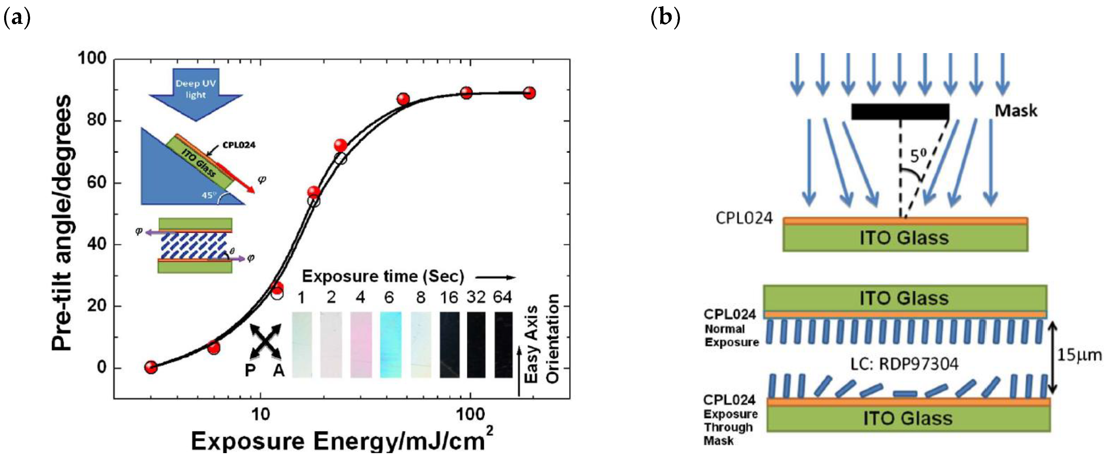
To prepare the surface of an LC lens, it must be coated with a photosensitive material (e.g., CPL024, from DIC Corporation). This compound represents a cross-linking polymer, providing a wide range of pretilt angles (1°–89°), which depend on the exposure energy (see
Figure 1a, where letters P and A denote polarizer and analyzer directions, respectively). The procedure of fabrication process includes the following steps: dissolution of the photoalignment material in a solvent (e.g., 0.5% wt/wt cyclohexanone) and then the solution is spin-coated on ITO substrates and obliquely exposed to UV light (
λ = 328 nm). This oblique exposure enables to set the pretilt angle as shown in
Figure 1b [
29]. By using the crystal rotation method, it is possible to measure the pretilt angles for the areas with differently absorbed exposure energy.
The bottom inset of
Figure 1a represents microphotographs of an LC cell with different pretilt angles vs. the exposure time (s). Thus, spatially changing UV irradiance is effective for obtaining any desired pattern.
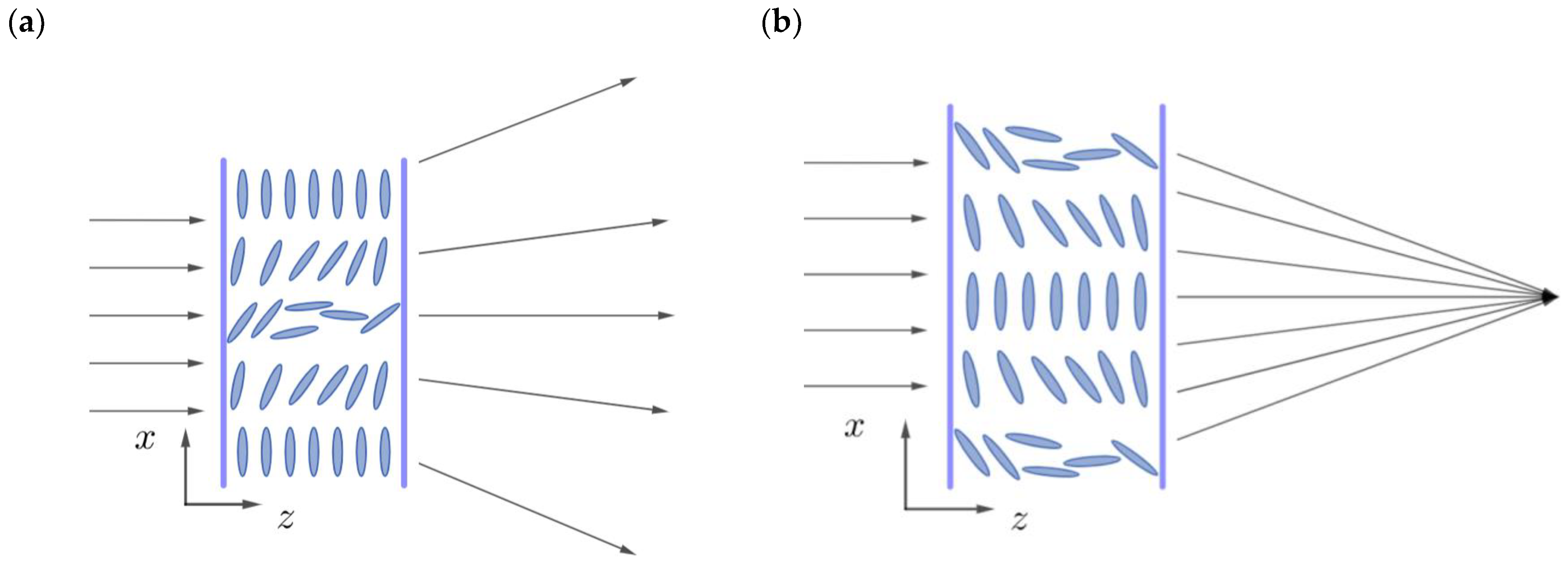
On the basis of the saturated dependence shown in
Figure 1a, it is clear that the center of the photosensitive surface of a diverging lens must absorb lower exposure energy than the outer areas. As a result, the radial distribution of the director has the form, which is depicted in
Figure 2a. If one irradiates the surface in the center with higher intensity than at the periphery, the resulting surface corresponds to a converging lens (see
Figure 2b). Once the surfaces are properly treated, the application of voltage to ITO-coated substrates leads to a change in the LC director configuration.
Optical power of the lens with large curvature radius
R can be evaluated by Fresnel’s formula [
30]:
where
λ is the wavelength, and ∆Φ is the phase shift between extraordinary waves passed through the center and the periphery of the lens. The phase of extraordinary wave is calculated as follows:
where
L is the path length,
corresponds to the principal refractive indices of LC, and angle
θ denotes the angle between wave vector
k and LC director (see
Figure 2b). In summary, Equations(1) and (2) show that the applied voltage results in a change in the spatial distribution of
and phase retardation
, which determines the focal distance [
28]. Relatively large lenses can have focal lengths of tens of centimeters. Small-sized lenses sustain focal spots at a distance of several tens of micrometers from the aligning surface.
Here it is important to note that spatially changing UV exposure results in the desired pattern. In addition, this methodology is applicable to beam steering devices. The ability to control the pretilt angle of LC molecules is a crucial step in the design of photonic devices.
2.1.2. Lenses with Non-Uniform Cell Thickness
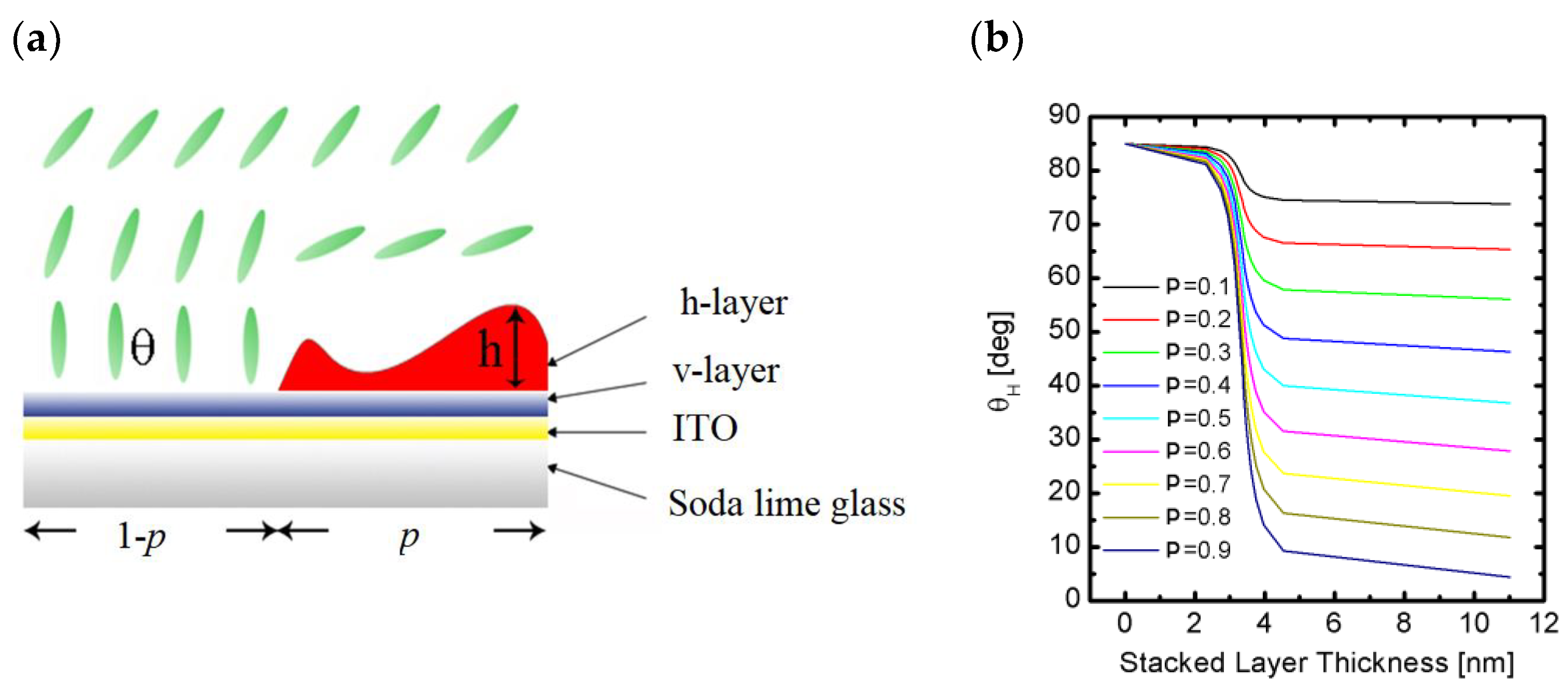
Manipulations with surface relief provide another way to achieve any desired phase profile. This approach is known as stacked alignment layers. It is associated with the change of the director’s azimuthal angle alignment by layering a homeotropic and planar alignment layer and selective removal of the upper layer. Lenses with non-uniform cell thickness consist of photoaligned horizontal polymer and rubbed vertical polyimide [
31]. A spatially changing pretilt angle is achieved by UV exposure of the stacked alignment layer. Lens-like phase retardation profile is achieved by a spatially changing pretilt angle. Consequently, the focal length of the LC lens becomes electrically tunable.
To obtain stacked alignment layers, a spin-coated polyimide for vertical alignment on the ITO substrate is required. Then, it must be cured and rubbed to provide the proper alignment. The angle between the rubbing direction and the transmission axes of polarizers should be 45°. In the next step, a polymer horizontal alignment (h-layer) is spin-coated on the polymer for vertical alignment. In order to polymerize the h-layer, it is exposed to UV light. Ultimately, a solvent (e.g., cyclohexanone) is used to rinse the unexposed h-layer. This final step results in a discontinuous alignment layer and it constitutes a nano-structured alignment layer (see
Figure 3a). Thus, the stacked alignment layer represents nanodomains with horizontally and vertically aligned materials. As a result, alignment surfaces comprise two domains favoring different LC orientations, which are characterized by the domain ratio:
, where
are the domain sizes with either vertical or horizontal alignment.
Control of the pretilt angle
θ is achieved by varying the ratio between the domain size and the extrapolation length of domain
i:
where
i denotes either horizontally or vertically aligned domain,
represents the splay elastic constant, and
is the polar anchoring energy of the domain. For typical alignment surfaces, the polar anchoring energy is 10
−4–10
−3 J/m
2. Consequently, its variation on the surface enables the manipulation of the LC structure within the bulk and anisotropic properties of the lens. Typical values of extrapolation length range within
The LC alignment is uniform for
. Otherwise, the alignment becomes inhomogeneous [
32].
As it can be seen from
Figure 3b, when the fraction of the domain length with horizontal alignment superiors the domain length with vertical alignment (e.g.,
p = 0.1), the pretilt angle does not change significantly when the thickness of stacked layers increases. Domination of vertical alignment (
) results in a decrease in the pretilt angle
θH as the stacked layer thickness increases.
The studies of atomic force microscopic images and continuum theory show that the mean pretilt angle
is fairly linear with respect to the domain ratio
p for
[
31]. This shows that the surface anchoring energy dominates elastic energy in the LC structure. Thus, the alignment of the pretilt angle on the
x-
y plane is controlled by the intensity of the UV source.
2.1.3. Lenses with Non-Uniform Electric Field
These lenses are fabricated using patterned electrodes. Nematic LCs or polymer-stabilized blue phase LC can be used as functional materials for such types of lenses [
33]. The application of a precalculated voltage results in a periodic gradient refractive index distribution. This method is equivalent to an anisotropic medium with a non-uniform thickness (see
Section 2.1.2).
2.2. Micropatterned Surface for Fresnel Lens
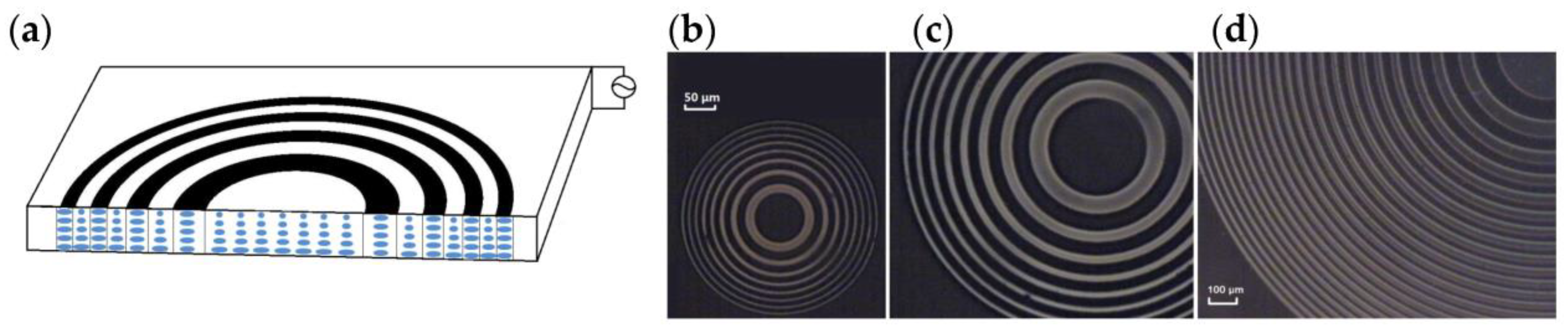
Combining a Fresnel zone electrode configuration with highly birefringent LC material leads to a flat, thin-film, phase retarder known as a Fresnel lens. The focusing properties of this lens are controlled by the electric field and characterized by high efficiency and quick response time. Orthogonal alignment of the domains can be achieved by using the photoalignment technique with the hybrid alignment of LCs. This means that electrically controlled birefringence and twisted nematic modes constitute electro-optical effects of the LC Fresnel lens. Bright circular rings correspond to twisted nematic mode and dark areas represent electrically controlled birefringence (see
Figure 4b–d). Detailed investigation of the beam profile shows that the lens achieves 42% diffraction efficiency with a switching time of about 6.7 ms [
34]. However, the theoretical limit of the diffraction intensity is about ~60%. In general, there are two factors that negatively impact the diffraction efficiency: the profile of the aligned structure and the effects of sharp edges on the LC. We believe that the non-contact alignment method reduces the negative contribution of the former effect. The imperfections in sharp edges on the liquid crystal are then transferred to the reduction in the diffraction intensity. In general, surface analysis is carried out by using optical microscopy and diffraction in the transmissive and reflective modes.
The achieved switching time and diffraction efficiency continue to superior other electrically tunable LC Fresnel plates, e.g., [
35,
36]. Furthermore, the Fresnel lens can also be assembled by using FLCs [
37]. In this case, the electro-optic response time is less than 0.1 ms for a voltage greater than 8 V. Thus, with the described characteristics, photoaligned Fresnel zone plates have significant potential for applications in advanced electro-optical devices.
3. Liquid Crystal Sensors
In this section, we reveal promising investigations on the design and application of LC-based sensors. Sensors are often defined as devices, which receive and respond to signals or stimuli. The latter represents the quantity, property, or condition, which is sensed and converted into a signal. For example, the sensing and visualization of temperature fields using cholesteric LCs are considered as traditional sensor applications of LCs. It is based on the high sensitivity of selective reflection spectra to temperature variations, which makes it possible to visualize temperature fields [
38]. This possibility is commonly used in biomedical applications of LCs for diagnostic pathology [
39]. Cholesteric LC and NLC were suggested for fiber optics pressure sensors and chemical and biological sensors, which currently attract strong interest. Thus, many research groups studied LC-based sensors due to their self-assembly potential and functional diversity [
22].
Several LC configurations for sensing applications are reviewed in the subsequent section.
3.1. Fiber Bragg Grating Sensor
Fiber Bragg gratings have inherent sensitivity to temperature changes, axial strain, and pressure. These changes are measurable as a shift of the Bragg wavelength in the reflected/transmitted power spectrum [
40].
Recent advances in nanomaterials, nanofabrication, and methods of LC photoalignment as fully integrated polarization-based photonic transducers were studied in ref. [
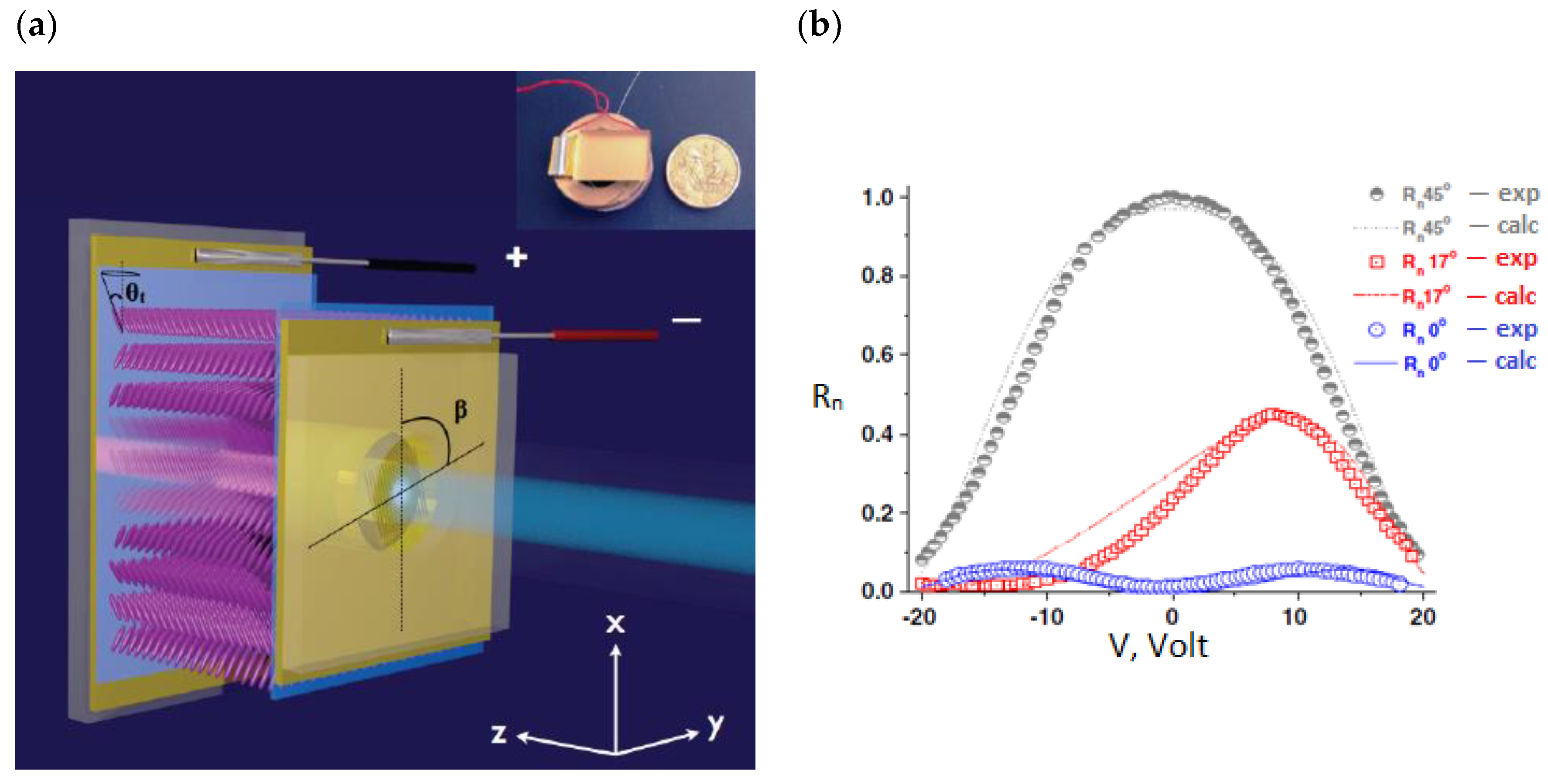
15]. The core of this study is the phase shift of the transmitted polarized light as a function of electric field in a deformed helix FLC cell. The corresponding sensor is depicted in
Figure 5a, where θ
t = 35° is the smectic tilt angle, and β is the angle between the helix axis and the polarization plane. The alignment of FLC with a submicron helix pitch is obtained by applying a 10 nm thick photoalignment layer on the gold electrode prior to filling the cell with the LC.
The working principle of the device is as follows: An optical fiber is glued to the top glass substrate. The glass substrate has an opening that fits a standard single-mode optical fiber, and a gold coating in front of the fiber tip is patterned to form a grid with a 200 nm period. A proper alignment of FLC is crucial for the device’s operation and it is achieved using photoalignment. Consequently, the light travels through the following layers: (1) the front gold electrode (−), which represents nanowire grid (in other words, it is a perfect polarizer); (2) photoaligned layer (light blue); (3) liquid crystal plate; (4) second alignment layer (light blue); (5) rear gold electrode (+), which represents a broad band mirror and reflects light into the fiber. The application of electric field along the z-axis (see
Figure 5a) leads to changes in the electrically controlled effective birefringence ∆
n and causes rotation of the optical axes by an angle Ω around the axis parallel to the electric field. Here, the function
is used to describe the reflectance of the LC cell, modulated by the applied voltage (see
Figure 5b) [
41]. This voltage-sensing reflective cell has continuous hysteresis-free optical phase shift and linearly polarized reflected light. The LC cell with the suggested design reflects light, which is modulated by the applied voltage. The latter can be measured by means of integrated single-mode fiber using unpolarized broadband light (
λ= 1.55 μm). Operating conditions are chosen in such a way to maximize the modulated reflectance and obtain linear response R
n(
V), which is crucial for sensor applications [
41,
42]. This effect is possible if the applied voltage ranges within ±3 V, and the reflected light intensity has a V-shaped response for β = 0.
3.2. Fiber-Optic Voltage Sensor
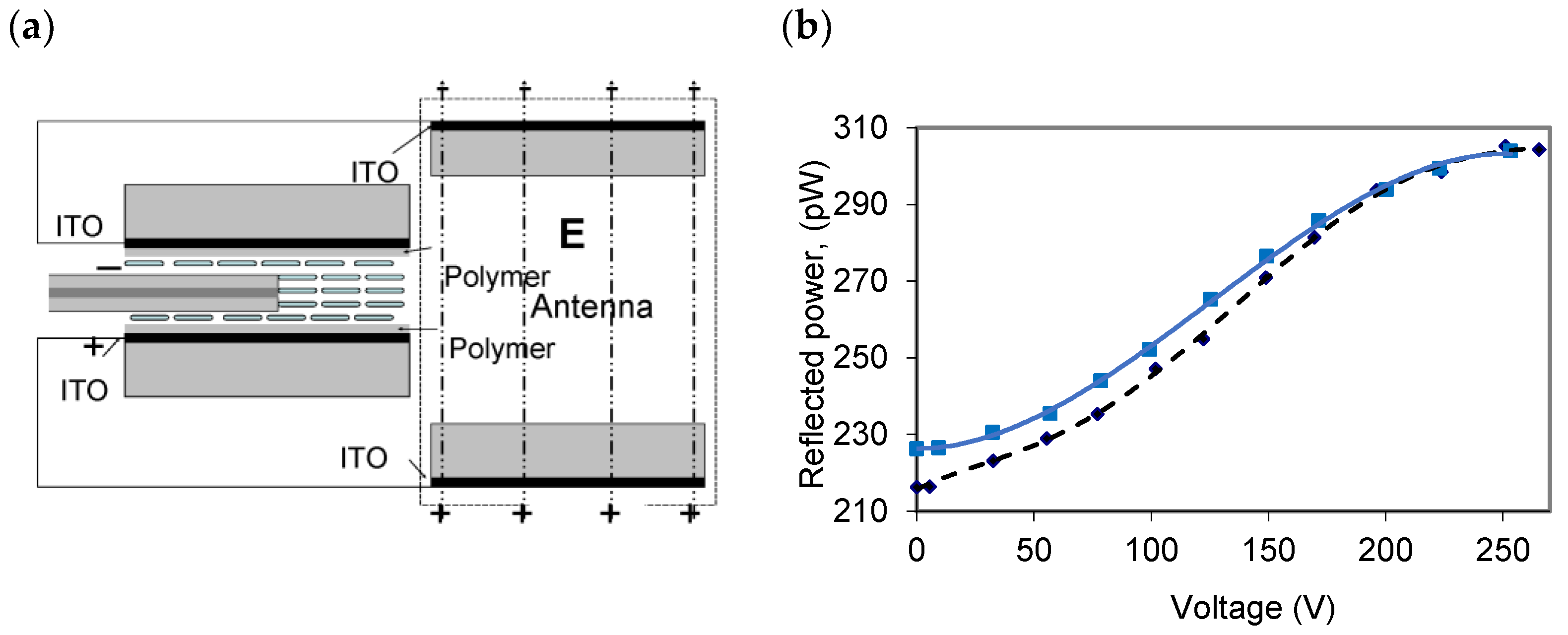
Optical transducers are easily installed into the existing equipment, and the availability of a wide range of optical sensors is important for prompt protection and voltage quality monitoring. This makes the development of voltage measurement techniques for high-voltage distribution systems (100–400 kV/m) extremely important. The idea behind a fiber-optic voltage sensor is the measurement of voltage by monitoring the electric-field-induced optical properties of hybrid fiber-optic devices. The device consists of two 3 dB 2X2 bi-directional couplers operating at 1550 nm and a fiber Bragg grating. A major characteristic of fiber Bragg grating is its ability to modulate the amplitude of refractive index change. This is achieved by a cleaved fiber end, which plays the role of a sensor head (see
Figure 6).
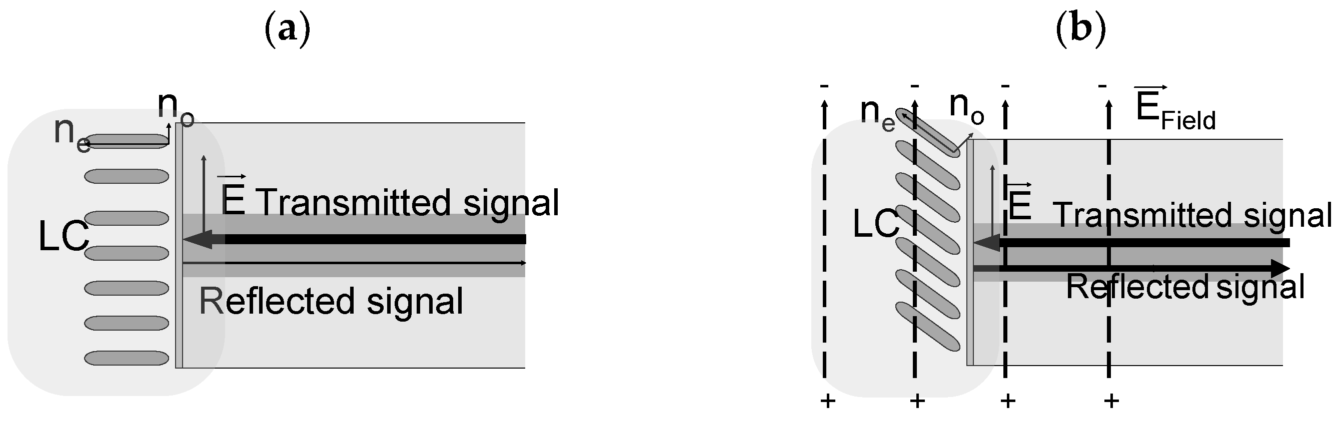
In the case of the proposed voltage sensor, the sensor head is immersed in planar-aligned LC, which is connected to an electric-field-sensing antenna (see
Figure 7) [
43]. The function of the sensor head is to monitor the optical properties of the LC. The sensor head surface plays the role of a broad-band mirror. Consequently, the incident light is reflected from the optical fiber surface, and the reflection coefficient varies depending on the applied voltage between the electrodes (see
Figure 7b).
The operating principle of the sensor relies on switching a 180 μm thick LC cell by the applied voltage of 260 V. The homeotropic alignment of LC molecules on the cleaved fiber (see
Figure 7a) is achieved by coating its surface with a polymer film.
Planar alignment of LC is achieved by the traditional rubbing method or photoalignment. Meanwhile, later investigations showed that photoalignment of nematic LC provides much better sensitivity to the external electric field. This is because the photoalignment of LC molecules results in a greater order parameter than it is achieved by rubbing alignment.
The intensity of the reflected light depends on the difference between the fiber-effective refractive index (
nF) and the LC-effective refractive index (
nLC). The latter depends on the angle between the polarization plane of light and the orientation of the LC director in the vicinity of the fiber surface (see
Figure 6b). The detected optical signal (“squares” and “diamonds” for the two couplers, see
Figure 7b) ranges within 216–306 pW.
This sensor can be used as a voltage controller in power-distributed systems. In particular, it can operate as a wavelength-division multiplexing system that multiplexes multiple optical carrier signals on a single optical fiber.
4. Optical Waveguides
Waveguide polarization LC devices represent a distinguished scientific interest. A combination of voltage-controlled anisotropic properties of LCs with specially shaped electrodes, pre-determined applied voltages, dielectric layers, and patterned alignment of liquid crystals results in the desired propagation of light. Below, we consider the layout of such low-voltage-controlled waveguide devices.
4.1. Optically Rewritable Technology
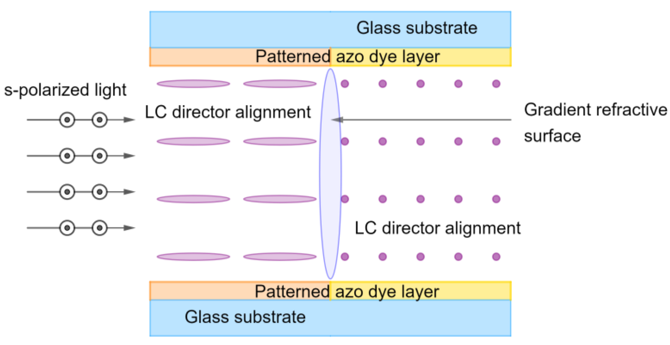
The optical path in LC devices highly depends on the surface properties and director alignment in the bulk. An example of a passive photonic device, in which a photoalignment layer induces gradient refractive interface, is shown in
Figure 8. Here, s-polarized light propagating in the bulk of the cell refracts from the gradient refractive interface [
44]. In other words, the incident s-polarized light beam from a waveguide is converted to the collimated beam within the LC bulk for further processing. Regarding p-polarized light, it undergoes total internal reflection at differently aligned domains.
The device depicted in
Figure 8 does not require an external voltage to maintain its alignment structure. There exist a variety of other prototype LC devices, which are based on photoalignment technology [
45]. A specific feature of photoaligned liquid crystal devices is their ability to be flexibly fabricated without electrodes [
46]. In this case, the cell gap is controlled by cylindrical pillars, and both experimental and theoretical studies confirm the insignificance of the relative area with the disordered surface alignment [
47].
4.2. Ferroelectric Liquid Crystal Fibers
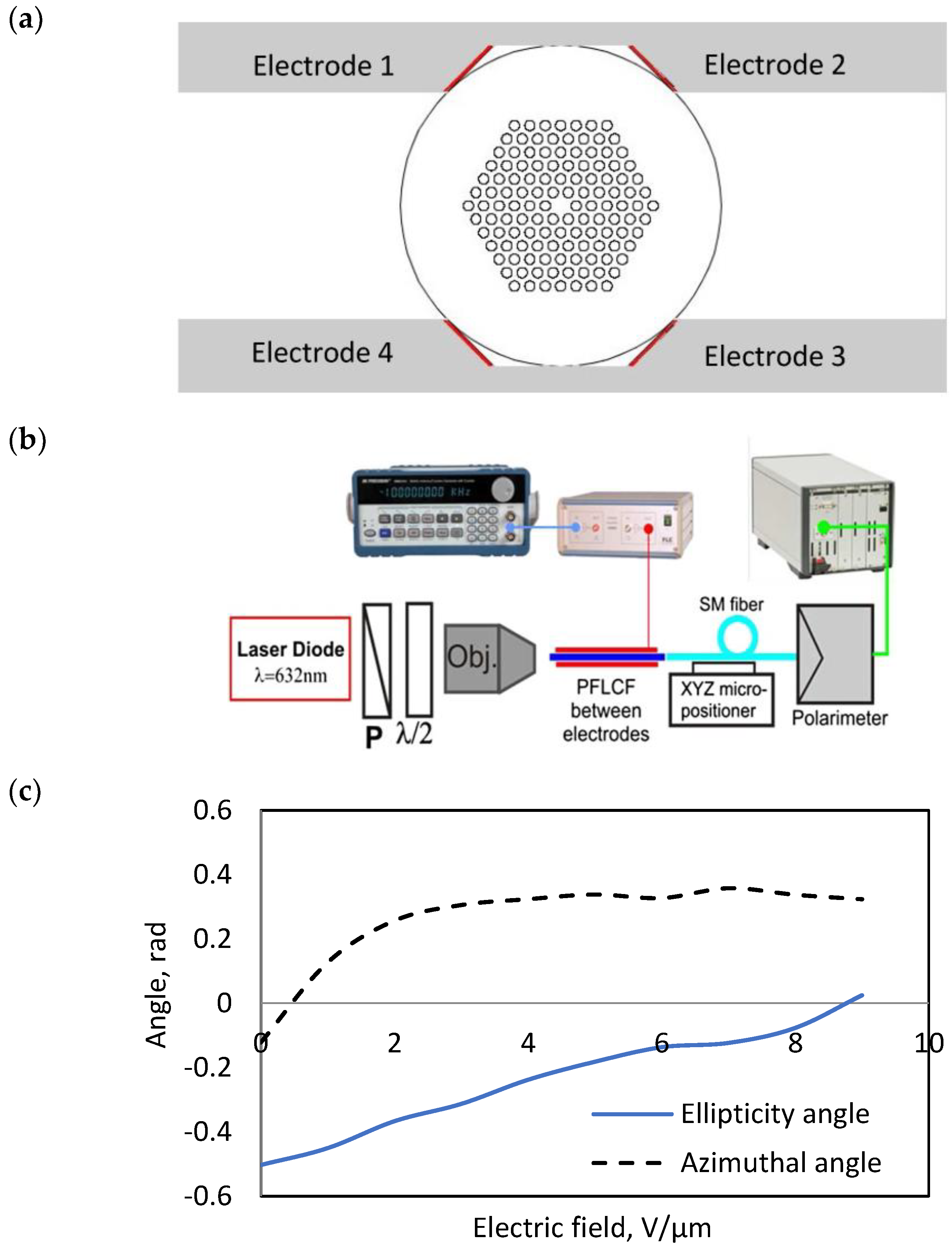
The effects of geometric phase modulation on molecular systems represent a specific scientific interest due to the transformation of the polarization state. This effect occurs when light passes through optically anisotropic structures, e.g., FLCs. In spite of dynamic phase modulation, which depends on the optical path length and frequency, geometric phase modulation is determined by the Poincaré sphere and Stokes parameter representation. The term “geometric phase modulation” has gained significance in practical applications, especially in fiber optics, where variable optical attenuation plays a key role. Below, we consider a device for controlling ellipticity.
Photonic crystals represent highly organized structures with submicron-scale periodicity. Current fabrication techniques are emerging at a fast pace; however, manufacturing large monocrystals still remains a challenge, and further work is necessary to achieve the precise orientation of large crystals. A way to solve this problem is to apply micropatterned photonic LC fibers. These fibers represent versatile optical waveguides with different geometries. D. Budaszewski et al. considered the application of photoaligned FLCs as functional materials to achieve quick electro-optic response in periodically arranged micro-channels. The fibers can be arranged in several ways, and an example of such geometry is shown in
Figure 9a [
48,
49].
The idea behind the setup shown in
Figure 9b is to control the state of polarization and obtain electrically tunable attenuation of the fiber. Here, a 7 cm long photonic crystal fiber (FLC FD4004N) with a diameter of ≈5 μm was obtained using photoalignment. The distance between electrodes was maintained at 126 μm. This means that
states of the director are possible along the fiber length (see the video, the link is provided in the Data Availability Statement). The photonic liquid crystal fiber birefringent axis was aligned parallel to the glass plates. A conventional narrow band laser diode (
λ = 632 nm) was used as the light source. A successive combination of the Glann–Thompson polarizer and a half-wave plate manifests change in the polarization state of the light. This system is supplemented by an objective for collimation of light. The cell was connected to the function generator with an amplifier. The application of an external electric field to the cell containing the fiber results in the continuous rotation of the optical axis and smooth change in the polarization state. The corresponding changes are measured by the Stokes polarimeter with a single-mode optical fiber.
The application of a square-shaped electric field with an amplitude ranging from 0 to 9 V/μm and a frequency of 1 kHz produces changes in the Stokes parameters (
). The response time is about 0.1 ms, and the degree of polarization is equal to 1. The investigation of the Stokes parameters vs. the voltage [
48] leads to the dependencies shown in
Figure 9c, where the ellipticity angle (
) and azimuthal angle (
) are calculated as follows:
Here, the sign of the ellipticity angle corresponds to left- and right-hand polarization, and we see that it ranges between −29° and 1.4°. Thus, one can attain small ellipticity for a phase modulator and saturation of the azimuthal angle. It is important to note that a small value of the ellipticity angle corresponds to linear polarization. In other words, the characteristics of rotation of the optical axis of FLC make it possible to agree refractive indices with the polarization state. Consequently, a photonic liquid crystal fiber represents a novel device for ellipticity control. A disappointing outcome of the device is the high electric field for practical applications. A way to solve this problem is to place electrodes closer to the FLC layer, i.e., fabricate conducting layers into empty photonic crystal fiber microchannels and apply the voltage to these layers.
5. Conclusions and Outlook
In this work, we reviewed several photonic LC devices employing photoalignment and various mechanisms for phase modulation. These mechanisms are refractive index modulation and thickness modulation technologies. Liquid crystalline structures are clearly important and bring new design rules for photonic devices. The main disadvantages of LC modulators are dispersion and sensitivity to polarization. We suggest that photosensitive azo dye would be an interesting candidate to solve the problem of minimum pixel size because the photoalignment technology enables to achieve domain size of less than 75 nm, but this range is beyond the limits of optical measurements. The alignment of a patterned surface in a single LC cell enables the independent optimization of the performance for orthogonal polarizations, whether they need to be identical or intentionally different. All these results are promising for the development and fabrication of LC photonic devices with photoinduced structures of long molecular axes.
Finally, it is worth noting that investigations of liquid crystals for display applications have achieved their maturation; however, liquid crystals for photonic applications are still open for research and new technologies. This is an exciting area of application, particularly in the following aspects: (1) development and investigation of novel photosensitive materials; (2) improving methods of photoaligned surface treatment; and (3) development of photonic devices for engineering applications.


