Review

Magnetic Force Microscopy of Multiferroic Bulk Ceramic Oxides

1
Electronic Ceramics Department, Jožef Stefan Institute, Jamova cesta 39, 1000 Ljubljana, Slovenia
2
Jožef Stefan International Postgraduate School, Jamova cesta 39, 1000 Ljubljana, Slovenia
3
Materials Research and Technology Department, Luxembourg Institute of Science and Technology, Rue du Brill 41, 4422 Belvaux, Luxembourg
*
Author to whom correspondence should be addressed.
Crystals 2023, 13(5), 838; https://doi.org/10.3390/cryst13050838
Submission received: 17 April 2023 / Revised: 10 May 2023 / Accepted: 16 May 2023 / Published: 19 May 2023
(This article belongs to the Special Issue Advanced Electronic Ceramics)

Abstract

:
Bulk multiferroic ceramics have been extensively studied due to their great potential for magneto-electric coupling applications such as low-power and multifunctional nano-electronic devices. In most of these studies the macroscopic magnetic performance was investigated, while the magnetic response on the micro- and nano-scale was not examined in detail. Local magnetic phenomena can be studied using magnetic force microscopy (MFM), a technique derived from atomic force microscopy. MFM measures the magnetic force between the magnetised tip and the magnetic sample. It is one of the most used methods to characterise the structure of ferromagnetic domains, because the sample preparation is simple, non-destructive and provides a relatively high-resolution image. In this review paper we focus on the MFM analyses of bulk multiferroic ceramics. The core of the article is divided into four sections: the introduction, the preparation of samples prior to MFM examination, the reviews of MFM analyses performed on bulk multiferroic ceramics with and without external magnetic fields, and finally the conclusions and an outlook for the future.

1. Introduction

Multiferroics are materials where ferroelectric and ferromagnetic, ferrimagnetic or antiferromagnetic ordering can coexist. Multiferroics in bulk ceramic form have a potential in multicaloric applications, which require large quantity of active materials, for example in future caloric cooling applications. Multicaloric effect could represent efficient solid state cooling by magnetic and electric fields in the future [1]. Readers seeking more information about multiferroics should refer to [2,3,4,5,6,7,8]. In this review, we focus on the magnetic domain structure of multiferroic oxide bulk ceramics studied by magnetic force microscopy (MFM). The question arises why there are not many MFM studies on multiferroic bulk ceramic materials. The answer lies in three reasons: (1) MFM is still not a widely spread characterization tool, (2) there are only a few multiferroics that exhibit multiferroic properties at room temperature [2,4] and (3) there are far less atomic force microscope (AFM) instruments that allow MFM analysis at cryogenic temperatures [9].
The MFM belongs to the group of scanning-probe microscopies, and dates back to the invention of the scanning-tunnelling microscope by Binnig and Rohrer in 1981. This won them the Nobel Prize in Physics, and was one of the triggers for the era of nanoscience. Five years later, Binnig, Quate and Gerber developed the AFM. From then on, various modes were developed and added to the AFM, e.g., magnetic force microscopy, piezo-response force microscopy, conductive AFM, and electrostatic force microscopy. The MFM was developed in 1987 [10,11].
The AFM consists of the AFM tip on a cantilever, a piezoelectric scanner, a photodiode, a data-acquisition unit and a controller (Figure 1a). The AFM tip, sometimes called the AFM probe, is a sensor that detects the interaction force, i.e., the van der Waals forces, between the tip and the surface of the sample being studied [12]. We can scan the surface in three different modes: contact mode, tapping mode and non-contact mode. In the first case the AFM tip is in hard contact with the surface. The surface topography is detected by the deflection of the cantilever from its original position, which is monitored by the reflection of a laser from the photodiode. When scanning in tapping mode, the AFM tip is periodically in contact or not with the surface of the sample. In non-contact mode, the tip has no contact with the surface at all and the surface is detected only by the long-range interaction forces between the tip and the sample [13].
In MFM, the interaction force is the magnetic force between the magnetised tip and the magnetic sample. In addition to magnetic interactions, van der Waals interaction forces are also present. These are responsible for the topography signal in the tapping and non-contact modes. The signal contains both magnetic and topographic information. To separate these two signals, the two-pass technique is normally applied. The dominant force depends on the distance of the tip from the sample. The van der Waals forces are short-range forces, while the magnetic forces act over longer distances between the tip and the surface (i.e., tens of nanometres). Therefore, by scanning images at different heights we can separate the magnetic and topographic signals. In the two-pass technique, the sample is scanned twice. In the first pass, the topography (i.e., a height profile) is determined, usually by tapping-mode scanning. In the second scan, the distance between the tip and the sample is increased, while the tip maintains the same height profile as in the first scan. In this way the distance and van der Waals interactions between the cantilever and the sample surface remain constant. In this case the tip is subject only to changes in the magnetic interactions, resulting in an MFM image. The principle of the two-pass MFM technique is shown in Figure 1b.
In the second scan when there are no magnetic interactions between the sample and the tip the cantilever oscillates with frequency v1, amplitude a1, and phase ϕ1. However, when a magnetic interaction occurs between the magnetic sample and the MFM tip, the cantilever starts to oscillate with frequency v2, amplitude a2, and phase ϕ2. Therefore, the change in the magnetic interaction is monitored by shifts in the frequency (Δv = v1v2), amplitude (Δa = a1a2), and phase (Δϕ = ϕ1ϕ2). Usually, an MFM image is presented as Δv or Δϕ scans. The changes in frequency and phase are related to the magnetic interactions between the tip and the sample (F) according to the following equations [9]:
Δ v v 1 2 k d F d z
Δ ϕ   Q k d F d z
where z is the cantilever displacement and Q and k are the quality factor and the spring constant of the cantilever, respectively. An overview of the different approaches to quantify MFM signals can be found here [9].
Figure 2 shows some examples of MFM frequency, amplitude and phase-signal images of a glass slide, a computer hard disk and a videotape. The glass is a non-magnetic material that serves as a reference material. As expected, only noise is observed in the MFM signals of the glass slide (Figure 2c–e). The MFM frequency, amplitude and phase images of the hard disk (Figure 2h–j) and videotape (Figure 2m–o) show magnetic features that are not related to the topographic height or any deflection of the sample surfaces (Figure 2f,g,k,l). The MFM scans of the hard disk and videotape show periodic magnetic domains, which is consistent with the literature [14,15]. The most sensitive rendition of the magnetic domain structure is achieved in MFM frequency images.
There are two options for the MFM tips: they can be made entirely of magnetic materials, such as iron, or they can be standard AFM tips that are coated with magnetic materials (e.g., CoCr, CoPt, FePt and NiFe alloys). Prior to the MFM measurements, the MFM tip must be magnetised to detect the magnetic interactions. Magnetisation can be achieved by bringing a permanent magnet close to a pristine MFM tip. To further confirm that the detected signal does indeed correlate with the magnetic properties of the material under investigation, an experiment can be performed with the opposite polarity of the tip (Figure 3a). Two scans of the same area can be performed. Before the first scan, the MFM tip is magnetised using a specific pole of the external magnet, while before the second scan, the MFM tip is magnetised with the opposite pole of the magnet. If the comparison of the two scans shows an inverted MFM signal, this is confirmation that the MFM signal results from the magnetic properties of the sample and is not due to crosstalk with the topography, an electrostatic contribution, or other experimental errors (Figure 3b). The removal of electrostatic artifacts by controlled magnetisation of the MFM tip is studied in more detail in [16].

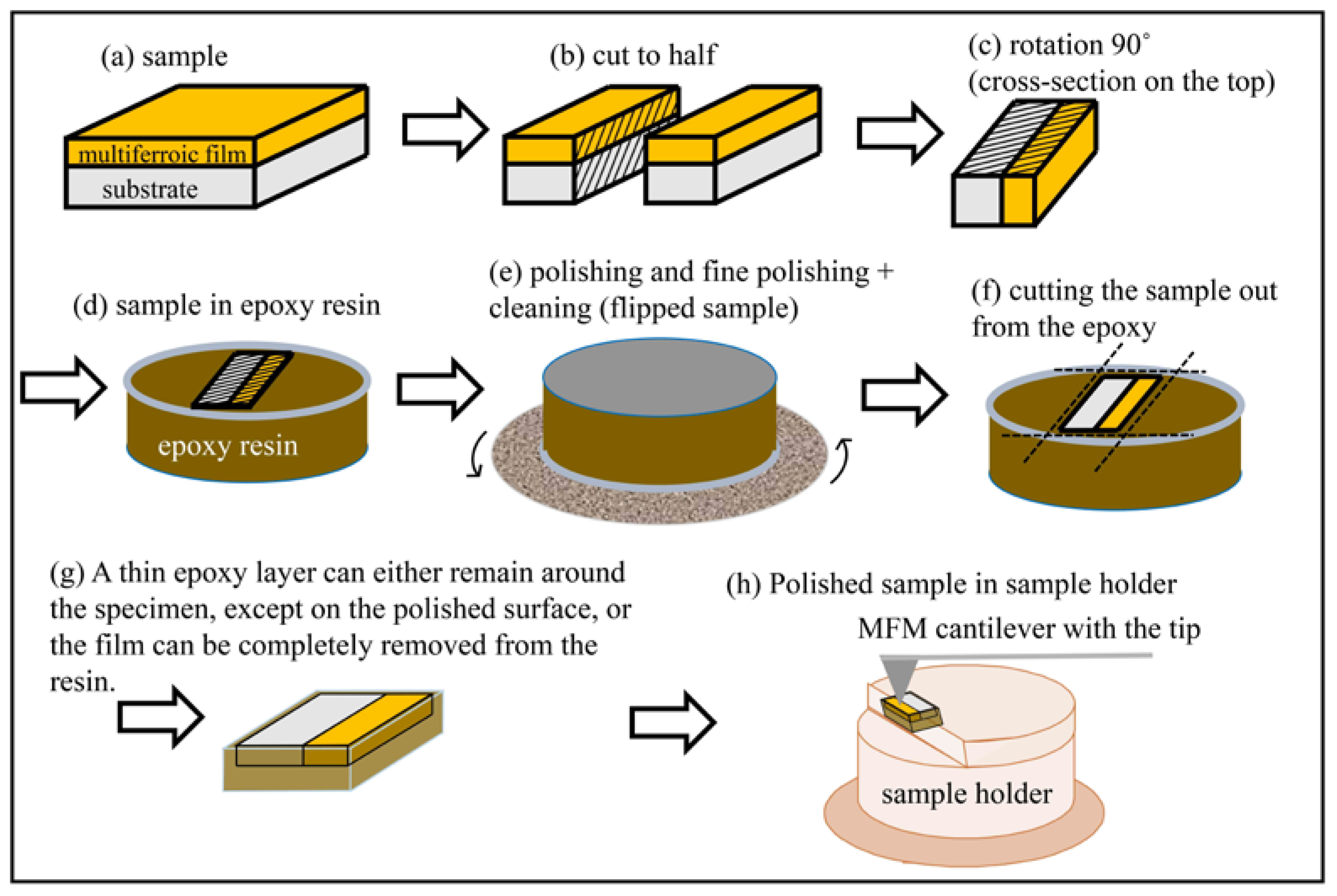
2. Polishing and Cleaning of Multiferroic Ceramic Specimens Prior to MFM Analysis

The MFM analysis of multiferroic thin films can be performed without pre-treatment [17,18,19,20,21], because the thin films are flat with the roughness below or in nanometre range. On the other hand, single crystals or bulk ceramics must be cut and polished [22,23,24,25]. Proper polishing and cleaning of crystal or ceramic samples are necessary to obtain the roughness of the samples below micrometre range and therefore to minimize the cross-talk of the MFM signal with the topography, leading to high-quality MFM images. A similar polishing-and-cleaning procedure for the bulk samples is also required for high-quality piezo-response force microscopy (PFM) images, as explained in [13].
The ceramics are usually cut to the correct dimensions and polished to obtain a flat surface for the MFM examination. The procedure requires several steps. The first is embedding the ceramic sample in polymer resin, for example in epoxy resin (Figure 4a), and grinding with silicon-carbide abrasive papers (5–20 μm SiC particles). The second step is polishing the sample on a cloth with a polishing paste, gradually reducing the size of the diamond abrasive to 0.25 μm. The third step is fine polishing with a colloidal SiO2 suspension containing particles down to tens of nanometres (Figure 4b) [22]. The bulk sample is then removed from the epoxy resin by heating so that the epoxy resin softens and the sample can be removed (Figure 4c,d). The sample is then prepared for MFM measurements (Figure 4e). One option is also to coat the surface of the multiferroic sample with a gold layer a few tens of nanometres thick to eliminate the electrostatic interactions between the ferroelectric domains and the MFM tip [26].
Surface contamination between the MFM tip and the multiferroic sample can interfere with the magnetic signal, as shown in Figure 5. The sample can be cleaned with an ultrasonic cleaner, UV ozone cleaner, lens-cleaning cloth or acetone, depending on the type of sample and the surface contaminants. Note, however, that acetone can leave stains on the surface of the sample. Removing contaminants is not always easy, so it is advantageous to work in a dust-free area such as a clean room.

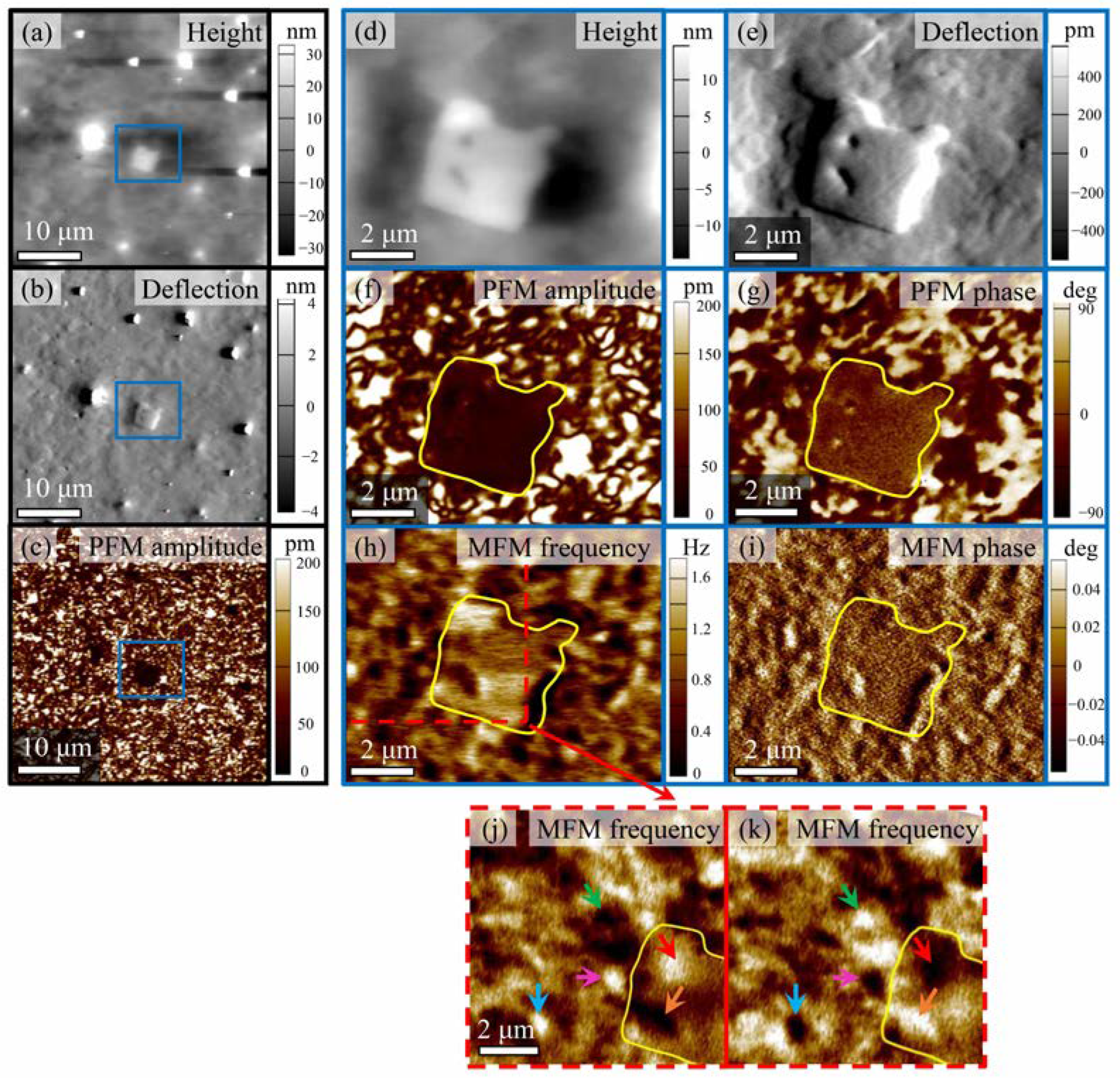
3. MFM Studies of Magnetic Domains in Multiferroic Bulk-Ceramic Samples

We focus here on the MFM of ceramic samples of multiferroic oxide. There are only a few studies on this topic [22,27,28,29,30], as discussed in more detail below. Other investigations deal with the MFM of multiferroic thin films [17,18,19,20,21,31,32,33], single crystals [25,26,34,35], nanowires [36,37], composites and heterostructures [23,24,27,38,39], all of which are beyond the scope of this review.
A large group of single-phase multiferroic materials is based on the bismuth ferrite BiFeO3 (BFO), which exhibits antiferromagnetic ordering with a Néel temperature of ~380 °C and ferroelectric behaviour with a ferroelectric Curie temperature of ~825 °C [40]. Rare-earth-element-modified BFOs are interesting because they can exhibit an enhanced ferromagnetic response compared to the parent BFO [22]. Their multiferroic domain structure, i.e., ferroelectric and magnetic domains, can be observed by PFM and MFM, as shown in Figure 6f–k for Bi0.88Gd0.12FeO3 ceramics. The PFM out-of-plane amplitude and phase images (Figure 6f,g) show the ferroelectric domain structure of the BFO matrix and the non-piezoelectric Fe-rich secondary phase. On the other hand, the MFM frequency and phase images show that both the BFO matrix and the Fe-rich secondary phase are magnetic (Figure 6h,i). As is shown here, microstructural analysis using MFM plays a crucial role in the characterization and interpretation of macroscopic magnetic measurements. The MFM experiment with opposite tip polarities (Figure 6j,k) shows an inverted MFM frequency signal (highlighted by the arrows) of the BFO matrix and the Fe-rich secondary phase, proving that the sample–tip interaction is indeed magnetic and not the result of topography or other non-magnetic phenomena.
A MFM analysis of the Li-modified BFO ceramic LixBi1−xFeO3 with x = 0.03 and x = 0.09 is also reported in the literature [27]. An X-ray diffraction analysis revealed that the Li0.09Bi0.91FeO3 ceramic prepared by convectional solid-state synthesis contains two secondary phases, namely LiFe5O8 (15 vol%) and Bi12.5Fe0.5O20 (6.2 vol%). MFM experiments on this sample revealed magnetic domains from nanometre to micrometre size. The density of the magnetic domains decreased with decreasing Li concentration from x = 0.09 to 0.03 [27]. In addition, a MFM analysis was performed on Bi0.85Sm0.15Fe0.97Sc0.03O3 ceramics prepared by hot pressing [28]. Long-range magnetic ordering was observed in these samples at room temperature (Figure 7). In a similar way, the long-range magnetic ordering was observed in Nd-modified BFO ceramics (Bi1-xNdxFeO3) with high Nd concentrations (x > 0.14) [29].
The microstructural investigation of bulk ceramics by MFM is very important to distinguish different phenomena between the matrix and the inclusions. A very interesting features in relaxor ferroelectrics are polar nanoregions that have the ability to form ferroelectric and magnetic regions, also known as multiferroic clusters (MFC) [30]. In relaxor ferroelectric single-phase (BiFe0.9Co0.1O3)0.4–(Bi1/2K1/2TiO3)0.6 ceramics, the MFC originate from magnetically strong Bi(Fe,Co)O3-rich regions with sizes in the range of 0.5–1.5 μm (Figure 8). Using the MFM technique a magnetic dipolar response of the MFC was confirmed by the switching an external (out-of-plane) magnetic field (±0.48 T) (Figure 8c–e). In addition, the MFM signal was altered by an in situ DC electric field (20 V) poling (Figure 8e,f, converse magnetoelectric effect). The direct magnetoelectric effect was also confirmed and even quantified for the MFC by using PFM and a variable external magnetic field [30].
One must be very careful when interpreting MFM results, especially when the experiment involves in situ electric field poling. Liu et al. [39] have used in situ electric field poling on thin film BiFeO3/La0.67Sr0.33MnO3 heterostructures, which resulted not only in a strong contrast of the PFM signal (Figure 9c), but also in a strong contrast of the MFM phase signal (Figure 9d). However, the “magnetic” signal of the MFM phase image does not originate from the electric-field-induced magnetization (converse magnetoelectric coupling), but from electrostatic interactions between the sample surface and the MFM tip, which arise due to the excess surface charges during the poling process. The electrostatic interactions were confirmed by scanning Kelvin probe microscopy (SKPM) in Figure 9e. Moreover, a solution to neutralize the excess surface charges was proposed, namely, scanning the poled region several times with a grounded tip in contact mode [39]. Although this example shows that excess surface charges are introduced into thin films by poling with an electric field, a similar phenomenon can also occur in polished bulk ceramic samples.

4. Magnetic-Force Microscopy Measurements under an Applied External Magnetic Field

Atomic force microscopes can be equipped with options for applying external magnetic fields to specimens, including out-of-plane and in-plane magnetic fields. With this option, the magnetic domain structure of the materials can be studied inside or outside the external magnetic field. Such a setup is shown schematically in Figure 10, where the magnetic field applied to the sample depends on the rotation angle of the magnet. When the angle of rotation is zero, the magnetic flux is deflected away from the sample. When the magnet is rotated 90°, the magnetic flux is directed through the sample [14,41].
Figure 11 shows MFM frequency images of the computer hard disk and the Bi0.88Gd0.12FeO3 bulk ceramic. The images were acquired at in-plane external magnetic fields from 0 G to 7000 G and −7000 G. The ferromagnetic domain structure of the hard disk remains unchanged up to 4300 G, while at a higher external magnetic field of 7000 G, the ferromagnetic domains switch and become more irregularly shaped. In contrast, the magnetic domains of the Bi0.88Gd0.12FeO3 bulk ceramic do not switch, even at the highest magnetic field of 7000 G. When we change the polarity of the external magnetic field (from 7000 G to −7000 G), we can observe an interesting phenomenon. The MFM experiment on the Bi0.88Gd0.12FeO3 bulk ceramic (Figure 11b, compare 7000 G and −7000 G) shows a complete inversion of the MFM frequency signal, while the shape of the magnetic domain structure remains the same. This indicates, first, that the MFM signal is related to the magnetic interaction between the sample and the tip, and not to the topography cross-talk [14], and, second, that switching of the in-plane external magnetic field causes a change in the polarity of the tip rather than the movements of the ferromagnetic domain walls of the Bi0.88Gd0.12FeO3. The domain structure of Bi0.88Gd0.12FeO3 ceramics is stable due to the high coercive magnetic field of this sample [22].

5. Conclusions and Outlook

Our understanding of the multiferroic properties of ceramic materials has improved in recent decades [4,5,6,7]. However, there are still many topics that require further research. These include (I) the coupling of the electromechanical and magnetic response in ceramic multiferroics and (II) multiferroic films in cross-section.
The first topic is important because it relates to the coupling of the electromechanical and magnetic responses in ceramic multiferroics at the nanoscale/microscale. An example of such an experiment is shown in Figure 12. The ferroelectric domain structure of the Bi0.88Gd0.12FeO3 bulk ceramic is shown in Figure 12a and is consistent with previous reports [22,42]. The contrasting bright and dark regions in the amplitude images correspond to areas with higher and lower piezoelectric responses. When the sample is subjected to an in-plane external magnetic field, as schematically shown in Figure 12g, the ferroelectric domain structure of the multiferroic Bi0.88Gd0.12FeO3 bulk ceramic does not change, even when the magnetic field is switched to the negative direction. This is related to the low magnetoelectric coefficients at room temperature [43,44] and the high coercive electric field of Gd-modified BiFeO3 ceramics [42].
The second idea for future work in this area is to study multiferroic thick films by MFM in cross-section. The procedure for preparing the thick film specimen prior to MFM examination differs slightly from the procedure for preparing the ceramic specimen shown in Figure 4. Therefore, Figure 13 shows a schematic of this idea. The multiferroic films can be cut in half (Figure 13b,c), embedded in epoxy resin (Figure 13d), and polished in cross-section (Figure 13e). After polishing, the surfaces of the specimens should be cleaned, preferably with distilled water, and dried in air. The specimens are removed from the cast by cutting away the epoxy resin around the films (Figure 13f,g). The specimen is placed in a specimen holder with a polished cross-sectional surface on top (Figure 13h). In the last step, MFM scanning should be performed on the cross-sectional surface. Using a PFM mode, a similar experiment was performed for ferroelectric thick films, where the ferroelectric properties of 0.65Pb(Mg1/3Nb2/3)O3–0.35PbTiO3 thick films in cross-section were investigated [45].
In conclusion, we believe that MFM analyses combined with other techniques such as piezo-response force microscopy, electrostatic force microscopy, conductive atomic force microscopy, thermal scanning microscopy and others, can lead to a deeper understanding and provide a link between the fundamental and functional properties of multiferroic ceramic materials and films at the nanoscale in the future.

6. Materials and Methods

Figure 2, Figure 3, Figure 5, Figure 11 and Figure 12 were scanned using MFP-3D and Jupiter XR atomic force microscopes, Oxford Instruments, Asylum Research, Santa Barbara, CA, USA. For MFM scanning, the two-pass MFM technique and Si tips coated with CoCr (ASYMFMHM, AtomicForce F&E GmbH, Mannheim, Germany) and Fe (ASYMFMLC, AtomicForce F&E GmbH, Germany) were used. PFM imaging was performed in dual AC resonance tracking mode. A voltage of 5 V and a frequency of ~350 kHz were used. Pt-coated silicon tips with a radius of curvature of ~10 nm (OMCL-AC240TM-R3, Olympus, Tokyo, Japan) were used.

Author Contributions

Conceptualisation, H.U.; methodology, H.U., M.Š., U.P. and V.F.; investigation, H.U., U.P. and V.F.; data curation, H.U., U.P. and V.F.; writing—original draft preparation, H.U.; writing—review and editing, H.U., M.Š., U.P. and V.F.; visualisation, H.U. and V.F.; supervision, H.U. All authors have read and agreed to the published version of the manuscript.

Funding

This work is funded by the Slovenian Research Agency in the frame of project N2-0212 and research core funding P2-0105.

Data Availability Statement

The data presented in this study are available upon request from the corresponding author.

Acknowledgments

The authors would like to thank Jena Cilenšek, Antonio Lisičak, Maria Karypidou for their help with the graphic design and Julian Walker for Bi0.88Gd0.12FeO3 bulk ceramic sample.

Conflicts of Interest

The authors declare no conflict of interest.

References

  1. Vopson, M.M. The multicaloric effect in multiferroic materials. Solid State Commun. 2012, 152, 2067–2070. [Google Scholar] [CrossRef]
  2. Eerenstein, W.; Mathur, N.D.; Scott, J.F. Multiferroic and magnetoelectric materials. Nature 2006, 442, 759–765. [Google Scholar] [CrossRef] [PubMed]
  3. Fiebig, M.; Lottermoser, T.; Meier, D.; Trassin, M. The evolution of multiferroics. Nat. Rev. Mater. 2016, 1, 16046. [Google Scholar] [CrossRef]
  4. Spaldin, N.A.; Ramesh, R. Advances in magnetoelectric multiferroics. Nat. Mater. 2019, 18, 203–212. [Google Scholar] [CrossRef] [PubMed]
  5. Jia, T.; Cheng, Z.; Zhao, H.; Kimura, H. Domain switching in single-phase multiferroics. Appl. Phys. Rev. 2018, 5, 021102. [Google Scholar] [CrossRef]
  6. Ramesh, R.; Manipatruni, S. Electric field control of magnetism. Proc. R. Soc. A 2021, 477, 20200942. [Google Scholar] [CrossRef]
  7. Evans, D.M.; Garcia, V.; Meier, D.; Bibes, M. Domains and domain walls in multiferroics. Phys. Sci. Rev. 2020, 5, 20190067. [Google Scholar] [CrossRef]
  8. Vopson, M.M. Fundamentals of Multiferroic Materials and Their Possible Applications. Crit. Rev. Solid State Mater. Sci. 2015, 40, 223–250. [Google Scholar] [CrossRef]
  9. Kazakova, O.; Puttock, R.; Barton, C.; Corte-León, H.; Jaafar, M.; Neu, V.; Asenjo, A. Frontiers of magnetic force microscopy. J. Appl. Phys. 2019, 125, 060901. [Google Scholar] [CrossRef]
  10. Martin, Y.; Wickramasinghe, H.K. Magnetic imaging by “force microscopy” with 1000 Å resolution. Appl. Phys. Lett. 1998, 50, 1455. [Google Scholar] [CrossRef]
  11. Sáenz, J.J.; García, N.; Grütter, P.; Meyer, E.; Heinzelmann, H.; Wiesendanger, R.; Rosenthaler, L.; Hidber, H.R.; Güntherodt, H.-J. Observation of magnetic forces by the atomic force microscope. J. Appl. Phys. 1987, 62, 4293–4295. [Google Scholar] [CrossRef]
  12. Sugawara, Y. Atomic Force Microscopy. In Roadmap of Scanning Probe Microscopy; Seizo Morita, Ed.; Springer: Berlin/Heidelberg, Germany, 2007; pp. 15–21. ISBN 978-3-540-34315-8. [Google Scholar]
  13. Uršič, H.; Prah, U. Investigations of ferroelectric polycrystalline bulks and thick films using piezoresponse force microscopy. Proc. R. Soc. A 2019, 475, 20180782. [Google Scholar] [CrossRef] [PubMed]
  14. Passeri, D.; Angeloni, L.; Reggente, M.; Rossi, M. Magnetic Force Microscopy. In Magnetic Characterization Techniques for Nanomaterials; Kumar Challa, S.S.R., Ed.; Springer: Berlin/Heidelberg, Germany, 2017; pp. 209–259. ISBN 9783662527801. [Google Scholar]
  15. Scheunert, G.; Cohen, S.R.; Kullock, R.; McCarron, R.; Rechev, K.; Kaplan-Ashiri, I.; Bitton, O.; Dawson, P.; Hecht, B.; Oron, D. Grazing-incidence optical magnetic recording with super-resolution. Beilstein J. Nanotechnol. 2017, 8, 28–37. [Google Scholar] [CrossRef]
  16. Angeloni, L.; Passeri, D.; Reggente, M.; Mantovani, D.; Rossi, M. Removal of electrostatic artifacts in magnetic force microscopy by controlled magnetization of the tip: Application to superparamagnetic nanoparticles. Sci. Rep. 2016, 6, 26293. [Google Scholar] [CrossRef]
  17. Gupta, S.; Pal, M.; Tomar, M.; Guo, R.; Bhalla, A.; Gupta, V. Ferroelectric and magnetic domain mapping of magneto-dielectric Ce doped BiFeO3 thin films. J. Alloys Compd. 2021, 882, 160698. [Google Scholar] [CrossRef]
  18. Jia, T.; Kimura, H.; Cheng, Z.; Zhao, H. Switching of both local ferroelectric and magnetic domains in multiferroic Bi0.9La0.1FeO3 thin film by mechanical force. Sci. Rep. 2016, 6, 31867. [Google Scholar] [CrossRef] [PubMed]
  19. Shimizu, K.; Kawabe, R.; Hojo, H.; Shimizu, H.; Yamamoto, H.; Katsumata, M.; Shigematsu, K.; Mibu, K.; Kumagai, Y.; Oba, F.; et al. Direct Observation of Magnetization Reversal by Electric Field at Room Temperature in Co-Substituted Bismuth Ferrite Thin Film. Nano Lett. 2019, 19, 1767–1773. [Google Scholar] [CrossRef]
  20. Gao, M.; Viswan, R.; Tang, X.; Leung, C.M.; Li, J.; Viehland, D. Magnetoelectricity of CoFe2O4 and tetragonal phase BiFeO3 nanocomposites prepared by pulsed laser deposition. Sci. Rep. 2018, 8, 323. [Google Scholar] [CrossRef]
  21. You, L.; Wang, B.; Zou, X.; Lim, Z.S.; Zhou, Y.; Ding, H.; Chen, L.; Wang, J. Origin of the uniaxial magnetic anisotropy in La0.7Sr 0.3MnO3 on stripe-domain BiFeO3. Phys. Rev. B 2013, 88, 184426. [Google Scholar] [CrossRef]
  22. Walker, J.; Mirjanic, A.; Prah, U.; Sadl, M.; Condurache, O.A.; Bencan, A.; Rojac, T.; Grigoras, M.; Ursic, H. Magnetic contributions in multiferroic gadolinium modified bismuth ferrite ceramics. Scr. Mater. 2020, 188, 233–237. [Google Scholar] [CrossRef]
  23. Shvartsman, V.V.; Alawneh, F.; Borisov, P.; Kozodaev, D.; Lupascu, D.C. Converse magnetoelectric effect in CoFe2O4–BaTiO3 composites with a core–shell structure. Smart Mater. Struct. 2011, 20, 075006. [Google Scholar] [CrossRef]
  24. Etier, M.; Shvartsman, V.V.; Gao, Y.; Landers, J.; Wende, H.; Lupascu, D.C. Magnetoelectric Effect in (0–3) CoFe2O4–BaTiO3(20/80) Composite Ceramics Prepared by the Organosol Route. Ferroelectrics 2013, 448, 77–85. [Google Scholar] [CrossRef]
  25. Jalli, J.; Hong, Y.K.; Abo, G.S.; Bae, S.; Lee, J.J.; Park, J.H.; Choi, B.C.; Kim, S.G. MFM studies of magnetic domain patterns in bulk barium ferrite (BaFe12O19) single crystals. J. Magn. Magn. Mater. 2011, 323, 2627–2631. [Google Scholar] [CrossRef]
  26. Geng, Y.; Lee, N.; Choi, Y.J.; Cheong, S.-W.; Wu, W. Collective Magnetism at Multiferroic Vortex Domain Walls. Nano Lett. 2012, 12, 6055–6059. [Google Scholar] [CrossRef]
  27. Sharma, Y.; Agarwal, R.; Collins, L.; Zheng, Q.; Ievlev, A.V.; Hermann, R.P.; Cooper, V.R.; KC, S.; Ivanov, I.N.; Katiyar, R.S.; et al. Self-Assembled Room Temperature Multiferroic BiFeO3–LiFe5O8 Nanocomposites. Adv. Funct. Mater. 2020, 30, 1906849. [Google Scholar] [CrossRef]
  28. Wang, C.; Yang, L.; Li, Z.; Zeng, M.; Zhang, A.; Qin, M.; Lu, X.; Gao, X.; Gao, J.; Lam, K.H. Giant room temperature multiferroicity and domain structures in hot-press sintered Bi0.85Sm0.15Fe0.97Sc0.03O3 ceramics. Ceram. Int. 2017, 43, 12764–12769. [Google Scholar] [CrossRef]
  29. Chen, J.; Xu, B.; Liu, X.Q.; Gao, T.T.; Bellaiche, L.; Chen, X.M. Symmetry Modulation and Enhanced Multiferroic Characteristics in Bi1−xNdxFeO3 Ceramics. Adv. Funct. Mater. 2019, 29, 1806399. [Google Scholar] [CrossRef]
  30. Henrichs, L.F.; Cespedes, O.; Bennett, J.; Landers, J.; Salamon, S.; Heuser, C.; Hansen, T.; Helbig, T.; Gutfleisch, O.; Lupascu, D.C.; et al. Multiferroic Clusters: A New Perspective for Relaxor-Type Room-Temperature Multiferroics. Adv. Funct. Mater. 2016, 26, 2111–2121. [Google Scholar] [CrossRef]
  31. Keeney, L.; Maity, T.; Schmidt, M.; Amann, A.; Deepak, N.; Petkov, N.; Roy, S.; Pemble, M.E.; Whatmore, R.W. Magnetic Field-Induced Ferroelectric Switching in Multiferroic Aurivillius Phase Thin Films at Room Temperature. J. Am. Ceram. Soc. 2013, 96, 2339–2357. [Google Scholar] [CrossRef]
  32. Faraz, A.; Maity, T.; Schmidt, M.; Deepak, N.; Roy, S.; Pemble, M.E.; Whatmore, R.W.; Keeney, L. Direct visualization of magnetic-field-induced magnetoelectric switching in multiferroic aurivillius phase thin films. J. Am. Ceram. Soc. 2017, 100, 975–987. [Google Scholar] [CrossRef]
  33. Li, L.; Lu, L.; Zhang, D.; Su, R.; Yang, G.; Zhai, J.; Yang, Y. Direct Observation of Magnetic Field Induced Ferroelectric Domain Evolution in Self-Assembled Quasi (0–3) BiFeO3–CoFe2O4 Thin Films. ACS Appl. Mater. Interfaces 2016, 8, 442–448. [Google Scholar] [CrossRef] [PubMed]
  34. Geng, Y.; Wu, W. Magnetoelectric force microscopy based on magnetic force microscopy with modulated electric field. Rev. Sci. Instrum. 2014, 85, 053901. [Google Scholar] [CrossRef] [PubMed]
  35. Geng, Y.; Das, H.; Wysocki, A.L.; Wang, X.; Cheong, S.-W.; Mostovoy, M.; Fennie, C.J.; Wu, W. Direct visualization of magnetoelectric domains. Nat. Mater. 2014, 13, 163–167. [Google Scholar] [CrossRef] [PubMed]
  36. Prashanthi, K.; Shaibani, P.M.; Sohrabi, A.; Natarajan, T.S.; Thundat, T. Nanoscale magnetoelectric coupling in multiferroic BiFeO3 nanowires. Phys. Status Solidi Rapid Res. Lett. 2012, 6, 244–246. [Google Scholar] [CrossRef]
  37. Prashanthi, K.; Thundat, T. In situ study of electric field-induced magnetization in multiferroic BiFeO3 nanowires. Scanning 2014, 36, 224–230. [Google Scholar] [CrossRef]
  38. Zavaliche, F.; Zheng, H.; Mohaddes-Ardabili, L.; Yang, S.Y.; Zhan, Q.; Shafer, P.; Reilly, E.; Chopdekar, R.; Jia, Y.; Wright, P.; et al. Electric Field-Induced Magnetization Switching in Epitaxial Columnar Nanostructures. Nano Lett. 2005, 5, 1793–1796. [Google Scholar] [CrossRef]
  39. Liu, C.; Ma, J.; Ma, J.; Zhang, Y.; Chen, J.; Nan, C.-W. Cautions to predicate multiferroic by atomic force microscopy. AIP Adv. 2017, 7, 055003. [Google Scholar] [CrossRef]
  40. Catalan, G.; Scott, J.F. Physics and Applications of Bismuth Ferrite. Adv. Mater. 2009, 21, 2463–2485. [Google Scholar] [CrossRef]
  41. Sylum Reasearch, “Variable Magnetic Field Module”. 2021. Available online: https://afm.oxinst.com/products/mfp-3d-other-driving-forces-acccessories/variable-magnetic-field-module (accessed on 27 March 2023).
  42. Walker, J.; Ursic, H.; Bencan, A.; Malic, B.; Simons, H.; Reaney, I.; Viola, G.; Nagarajan, V.; Rojac, T. Temperature dependent piezoelectric response and strain-electric-field hysteresis of rare-earth modified bismuth ferrite ceramics. J. Mater. Chem. C 2016, 4, 7859–7868. [Google Scholar] [CrossRef]
  43. Tryhuk, V.V.; Ravinski, A.F.; Makoed, I.I.; Lazenka, V.V.; Januszkiewicz, K.I. Magnetoelectric Coupling and Lattice Dynamics of Gd-Doped BiFeO3 Multiferroics. In Proceedings of the IEEE International Conference on Oxide Materials for Electronic Engineering (OMEE), Lviv, Ukraine, 3–7 September 2012; pp. 253–254. [Google Scholar]
  44. Pattanayak, S.; Choudhary, R.N.P.; Shannigrahi, S.R.; Das, P.R.; Padhee, R. Ferroelectric and ferromagnetic properties of Gd-modified BiFeO3. J. Magn. Magn. Mater. 2013, 341, 158–164. [Google Scholar] [CrossRef]
  45. Ursic, H.; Sadl, M. Investigation of piezoelectric 0.65Pb(Mg1/3Nb2/3)O3–0.35PbTiO3 films in cross section using piezo-response force microscopy. Appl. Phys. Lett. 2022, 121, 192905. [Google Scholar] [CrossRef]
Figure 1. (a) Example of AFM system adapted for MFM measurements. (b) Schematic of the MFM measurement principle.
Crystals 13 00838 g001
Figure 2. AFM topographic height, deflection and MFM frequency v, amplitude a and phase ϕ signal images of (ae) glass slide, (fj) computer hard disk (Maxtor D740X-6L 40GB HDD) and (ko) videotape.
Crystals 13 00838 g002
Figure 3. (a) Schematic of the experiment with different tip polarities. (b) AFM topographic height and deflection images and MFM frequency images of a computer hard disk. The green rectangle highlights a region where an experiment with opposite magnetic tip polarities was performed. The pairs of coloured dashed brackets represent the same region with an inverted MFM signal.
Crystals 13 00838 g003
Figure 4. Schematic of a multiferroic bulk ceramic sample’s preparation prior to MFM investigation.
Crystals 13 00838 g004
Figure 5. (a) AFM topography height and MFM (b) frequency and (c) phase images of a Bi0.88Gd0.12FeO3 multiferroic ceramic containing an Fe-rich secondary phase after polishing with a paste on a cloth and fine polishing with a colloidal SiO2 suspension. Some examples of dust particles on the sample surface are marked with red arrows.
Crystals 13 00838 g005
Figure 6. (a,b) AFM topography height and deflection and (c) PFM amplitude images of Bi0.88Gd0.12FeO3 bulk ceramics. The blue square marks a region of Fe-rich secondary phase, magnified in panels (di) and indicated by a yellow line. Panels (f,g) show PFM amplitude and phase images, and (h,i) show MFM frequency and phase images of this region. Panels (j,k) show MFM frequency of a region where an experiment with opposite magnetic tip polarities was performed [22]. Copyright 2020 Elsevier (Creative Commons CC-BY license).
Crystals 13 00838 g006
Figure 7. MFM analysis of Bi0.85Sm0.15Fe0.97Sc0.03O3 ceramics. (a) AFM topography, MFM (b) amplitude and (c) phase images [28]. Copyright 2017 Elsevier.
Crystals 13 00838 g007
Figure 8. MFM measurements of MFC in relaxor ferroelectric single-phase (BiFe0.9Co0.1O3)0.4–(Bi1/2K1/2TiO3)0.6 ceramics in combination with external magnetic field (H) and electric field (E) poling. (ac) MFM phase images of the MFC (a) before and (b,c) after ex situ switching with out-of-plane magnetic fields of ±0.48 T as indicated by blue arrows. The symbols above the images represent single magnetic domains according to the dipolar magnetic MFM response. (e,f) PFM images of MFC recorded after ex situ magnetic switching, (e) before and (f) after electric field (20 V) poling by scanning a rectangular area as indicated by the red dashed rectangle. Configurations of MFC’s polarization are illustrated by symbols below the PFM images. (d) MFM phase image after electric field poling, showing magnetoelectric switching [30]. Copyright 2016 Wiley.
Crystals 13 00838 g008
Figure 9. (a) AFM topography image and (b) MFM phase image of thin film BiFeO3/La0.67Sr0.33MnO3 heterostructure in the initial state. Figures (ce) show (c) out-of-plane PFM phase image, (d) MFM phase image and (e) SKPM potential image, respectively, after double-box polarization. Scale bars represent 1 μm [39]. Copyright 2017 AIP Publishing.
Crystals 13 00838 g009
Figure 10. Schematic of the experimental setup for (a,b) out-of-plane and (c,d) in-plane magnetic field measurements. When the rotation angle of the magnet is zero, no external magnetic field is applied to the sample, as shown in panels (a,c). After the magnet is rotated 90°, the sample is brought into the external magnetic field, as shown in panels (b,d).
Crystals 13 00838 g010
Figure 11. MFM frequency images under external in-plane magnetic fields for (a) computer hard disk (Maxtor D740X-6L 40GB HDD) and (b) Bi0.88Gd0.12FeO3 bulk ceramics. Measurements were performed using an AFM Jupiter, Asylum Research, Santa Barbara, USA with a MFM tip Asymfmlc-R2. The white square is only a guide for the eyes.
Crystals 13 00838 g011
Figure 12. Piezo-response force microscopy of Bi0.88Gd0.12FeO3 bulk ceramics in an external in-plane magnetic field. (af) PFM out-of-plane amplitude image under external in-plane magnetic field from 0 to ±8000 G. (g) Schematic representation of the setup for PFM measurements in a magnetic field. (h) Enlarged view of the areas marked by the white square in panels (a,f).
Crystals 13 00838 g012
Figure 13. Schematic of a multiferroic thick-film sample’s preparation prior to MFM cross-section investigation.
Crystals 13 00838 g013
Disclaimer/Publisher’s Note: The statements, opinions and data contained in all publications are solely those of the individual author(s) and contributor(s) and not of MDPI and/or the editor(s). MDPI and/or the editor(s) disclaim responsibility for any injury to people or property resulting from any ideas, methods, instructions or products referred to in the content.

