Article

N-Polar Indium Nitride Quantum Dashes and Quantum Wire-like Structures: MOCVD Growth and Characterization

1
Materials Department, University of California, Santa Barbara, CA 93106, USA
2
Electrical and Computer Engineering Department, University of California, Santa Barbara, CA 93106, USA
*
Author to whom correspondence should be addressed.
Crystals 2023, 13(4), 699; https://doi.org/10.3390/cryst13040699
Submission received: 27 February 2023 / Revised: 14 April 2023 / Accepted: 18 April 2023 / Published: 19 April 2023

Abstract

:
The electrical properties of InN give it potential for applications in III-nitride electronic devices, and the use of lower-dimensional epitaxial structures could mitigate issues with the high lattice mismatch of InN to GaN (10%). N-polar MOCVD growth of InN was performed to explore the growth parameter space of the horizontal one-dimensional InN quantum wire-like structures on miscut substrates. The InN growth temperature, InN thickness, and NH3 flow during growth were varied to determine optimal quantum wire segment growth conditions. Quantum wire segment formation was observed through AFM images for N-polar InN samples with a low growth temperature of 540 °C and 1–2 nm of InN. Below 1 nm of InN, quantum dashes formed, and 2-D layers were formed above 2 nm of InN. One-dimensional anisotropy of the electrical conduction of N-polar InN wire-like samples was observed through TLM measurements. The sheet resistances of wire-like samples varied from 10–26 kΩ/□ in the longitudinal direction of the wire segments. The high sheet resistances were attributed to the close proximity of the treading dislocations at the InN/GaN interface and might be lowered by reducing the lattice mismatch of InN wire-like structures with the substrate using high lattice constant base layers such as relaxed InGaN.

1. Introduction

The III-nitride semiconductor system of GaN, AlN, and InN is a promising platform for next-generation electronics due to its favorable material properties such as high electron mobilities, high thermal conductivities, and high breakdown voltages. InN, which is normally utilized for InGaN-based visible and ultraviolet optoelectronics [1,2,3,4], has interesting electrical properties. These properties include a low electron effective mass of 0.07 m0, leading to the highest theoretical mobilities of the III-nitrides of up to 14,000 cm2 V−1 s−1 at 300 K and the highest electron saturation drift velocity of the III-nitrides [5,6]. InN also features a high electron surface accumulation [7], which has applications in chemical sensing [8,9]. These electrical properties make InN an intriguing choice for electronic devices.
Despite the potential InN has for electronics applications, its performance has fallen short of theoretical limits because of the challenges involved in achieving high quality epitaxial material. InN has an extremely high in-plane lattice mismatch to available substrates, including 10% to GaN and 25% to sapphire, resulting in a 3D (Volmer–Weber) growth mode and very high dislocation densities of up to 1010 cm−2 at InN/GaN interfaces [5]. InN grown on GaN is fully relaxed, even for thicknesses as low as 1 nm, and forms misfit dislocations at the InN/GaN interface that have been observed and studied in the literature [10,11,12]. In addition to the high lattice mismatch challenges, due to its high equilibrium N2 vapor pressure, InN must be grown at very low temperatures compared to GaN in common epitaxial techniques such as molecular beam epitaxy (MBE) and metalorganic chemical vapor deposition (MOCVD) [13,14]. The ideal MOCVD growth temperatures for GaN are above 1000 °C, while InN is grown at temperatures between 450 °C and 650 °C, above which temperature InN will decompose [5]. Growth at low temperatures results in increased impurity incorporations and reduced structural quality. In addition, ammonia (NH3), the most common nitrogen precursor for MOCVD growth of III-nitrides, suffers from greatly reduced pyrolysis efficiency at temperatures below 900–1000 °C due to the strength of the N-H bond [15].
A possible path toward achieving high performance MOCVD-grown InN material is the use of lower dimensional epitaxial structures such as 0D quantum dots and 1D quantum wires, which have applications in optoelectronics and electronics such as light-emitting diodes, lasers, and transistors [16,17,18,19,20]. The quantum confinement provided by such structures leads to enhanced carrier confinement and reduced sensitivity of material properties to changes in temperature and structural defects [21,22]. The decreased defect sensitivity of lower dimensional structures is especially attractive because it could enable effective devices in large lattice mismatch systems such as InN/GaN that normally suffer from defect-induced degradations of transport properties. InN quantum dots have been grown epitaxially by MOCVD and molecular beam epitaxy (MBE), demonstrating signatures of quantum confinement such as blue-shifted photoluminescence (PL) peak wavelengths and temperature-insensitive optical properties [23,24,25]. The InN quantum dot results from the literature indicate that using quantum confinement improves the performance of InN for optoelectronics. However, quantum dots are not suitable for electronics applications as charge carriers are typically confined to the dots and, therefore, have highly reduced mobility; thus, 1D quantum wires come into consideration as charge carriers have plane wave character and potentially high mobility one dimension. InN quantum wires and nanowires grown by various methods have been achieved with 1D transport properties [26,27,28,29,30,31,32,33]. Some of the most outstanding results arise from studies of MBE-grown freestanding InN nanowires on Si (111) substrates [27,31,33]. The InN wires were 0.7–4 µm tall with free carrier concentrations as low as 1 × 1013 cm−3 and extracted room temperature electron mobilities of up to 12,000 cm2 V−1 s−1, which approaches the theoretical mobility values for InN [33]. The enhanced performance was attributed to reduced structural defects in the wires. Based on the MBE results, it appears that the epitaxial growth of InN wires with 1D electrical conduction has the potential to widen the design and application flexibility for III-nitride electronics as well as unlock the true potential of InN.
While there has been significant research effort towards vertical InN quantum wires, there is less prior work on horizontal InN wire arrays that could be more easily incorporated into full epitaxial devices. It has been previously shown in several III-V semiconductor systems that vicinal or high-index substrates enable the epitaxial growth of horizontal quantum wires with 1D optical and electrical properties [34,35,36,37,38,39,40,41]. Such substrates in the III-arsenides system include high-index (311) A GaAs and miscut (100) and (110) GaAs [35,36,37]. For the III-nitrides, a horizontal quantum wire formation has been observed in MOCVD-grown N-polar AlGaN/GaN heterostructures on miscut sapphires [38,40,41,42,43]. Vicinal sapphire substrates with miscut angles in the range of 2–5° have been found to suppress hexagonal hillock formation during N-polar III-nitride MOCVD growth, resulting in smooth, high-quality films [43]. N-polar AlGaN/GaN heterostructures grown on these sapphire substrates with tuned growth conditions exhibited lateral carrier confinement along the surface step direction, anisotropic charge distribution, electron mobility, and optical polarization [38,40,41]. Thus, the use of such substrates is a promising method towards the growth of horizontal InN quantum wires.
N-polar III-nitride MOCVD growth on miscut substrates also provides benefits for InN quantum structures intended for epitaxial device stacks. While capping MOCVD-grown metal-polar InN quantum dots with GaN formed conformal caps rather than planarized layers [44], which inhibited the direct epitaxial growth of full device stacks, N-polar MOCVD-grown InN grown on miscut GaN was found to form quantum dashes rather than dots, and the dashes elongated along the direction of the surface steps [45]. GaN cap layers grown on top the dashes exhibited planarized surfaces, even with multiple layers of dashes, enabling the growth of additional device layers on such structures [24,45]. Both uncapped and capped InN quantum dashes showed pronounced infrared luminescence [24]. In addition, just 20 nm thick MOCVD-grown N-polar InN films exhibited electron mobilities of up to 706 cm2 V−1 s−1 [45]. Thus, the N-polar orientation provides several benefits for approaching horizontal InN quantum wires, planarized GaN capping capability, and additional benefits to electronic performance from the reversed polarization fields that make the N-polar orientation a natural choice for III-nitride electronics applications [46,47]. By carefully tuning the MOCVD growth conditions of N-polar InN, it may be possible to elongate the quantum dashes into horizontal quantum wire arrays and achieve 1D conduction.
In this work, the growth parameter space of MOCVD-grown horizontal N-polar InN quantum wire-like structures on GaN was investigated using morphological and electrical measurements. It was found that a low temperature of 540 °C with a narrow thickness window of 1 nm–2 nm was required to form InN quantum wire segments rather than dashes. Fabricated InN wire segment samples were electrically conductive with sheet resistances of 10–26 kΩ/□ along the wire segment direction, with much higher sheet resistances perpendicular to the wire segment direction. The InN could be capped with a thin layer of GaN while retaining electrical conduction. The results of this work demonstrate the possibility of control over the dimensionality of lower-dimensional InN epitaxial structures while establishing the performance limits of such structures on GaN.

2. Methods

N-polar InN quantum wire-like structure samples were grown by atmospheric pressure MOCVD on 2-inch diameter sapphire substrates, with a miscut of 4° toward the a-direction (4A), which resulted in GaN surface steps parallel to the a-direction [42,43]. Ammonia (NH3) was used as the nitrogen precursor, and trimethylindium (TMIn), trimethylgallium (TMGa), and triethylgallium (TEGa) were used as the metalorganic precursors. InN growth rates were calibrated using InN deposition on Si (111) substrates. All InN quantum dash and quantum wire-like structure growths started with the deposition of a 20 nm thick GaN buffer layer grown at 1060 °C, with precursor flows of 12 μmol min−1 of TMGa and 45 mmol min−1 of NH3, followed by a 2 μm thick semi-insulating GaN template grown at 1200 °C using 40 μmol min−1 of TMGa and 45 mmol min−1 of NH3, as reported previously [45]. InN was deposited on top at growth temperatures of 540–640 °C with 0.6 μmol min−1 TMIn and 143 mmol min−1 NH3, and any GaN caps over the InN were grown using 1.5 μmol min−1 TEGa and 143 mmol min−1 NH3. The GaN base layers characterized by X-ray diffraction exhibited FWHM values of 311 arcsec for the 000 2 ¯ reflection and 340 arcsec for the 20 2 ¯ 1 ¯ reflection. These values correspond to dislocation densities in the mid 108 cm−2 range [43]. The polarity of the GaN base layers was confirmed previously [43]. All layers after the initial GaN template were grown with N2 as the carrier gas. Several experimental series were drawn to investigate the effects of the InN growth temperature, InN thickness, NH3 flow, and cap growth temperature and thickness on the formation and properties of the InN quantum wire-like structures. The capping of InN on select samples was investigated as well. In the growth temperature series, nominally, 1 nm of InN was deposited on the semi-insulating templates at temperatures between 540 °C and 640 °C. In the InN thickness series, nominally, 0.5 nm–20 nm of InN was deposited at 540 °C. In the NH3 flow series, nominally, 1 nm of 540 °C InN was deposited with NH3 flows between 0.5 SLM and 6 SLM. Capped samples included 6 nm of TEGa-grown GaN grown entirely at 540 °C, partially at 540 °C, partially at 640 °C, or entirely at 640 °C. Figure 1 shows the epitaxial structure of uncapped InN samples.
InN growth rate calibration samples on Si were measured using ellipsometry. The N-polar InN samples and GaN template were characterized by atomic force microscopy (AFM) to assess surface morphology. Room temperature Hall measurements were performed on thicker InN film samples (20 nm thick InN) to measure electron concentrations and mobilities. Hall measurements were conducted using a Van der Pauw configuration on cleaved 1 × 1 cm pieces and pressed indium dot contacts. Selected samples were fabricated with transmission line measurement (TLM) structures parallel and perpendicular to the InN wire-like structure direction to measure sheet resistance. The fabrication process included a BCl3/Cl2—based mesa etch and Al/Au ohmic contacts.

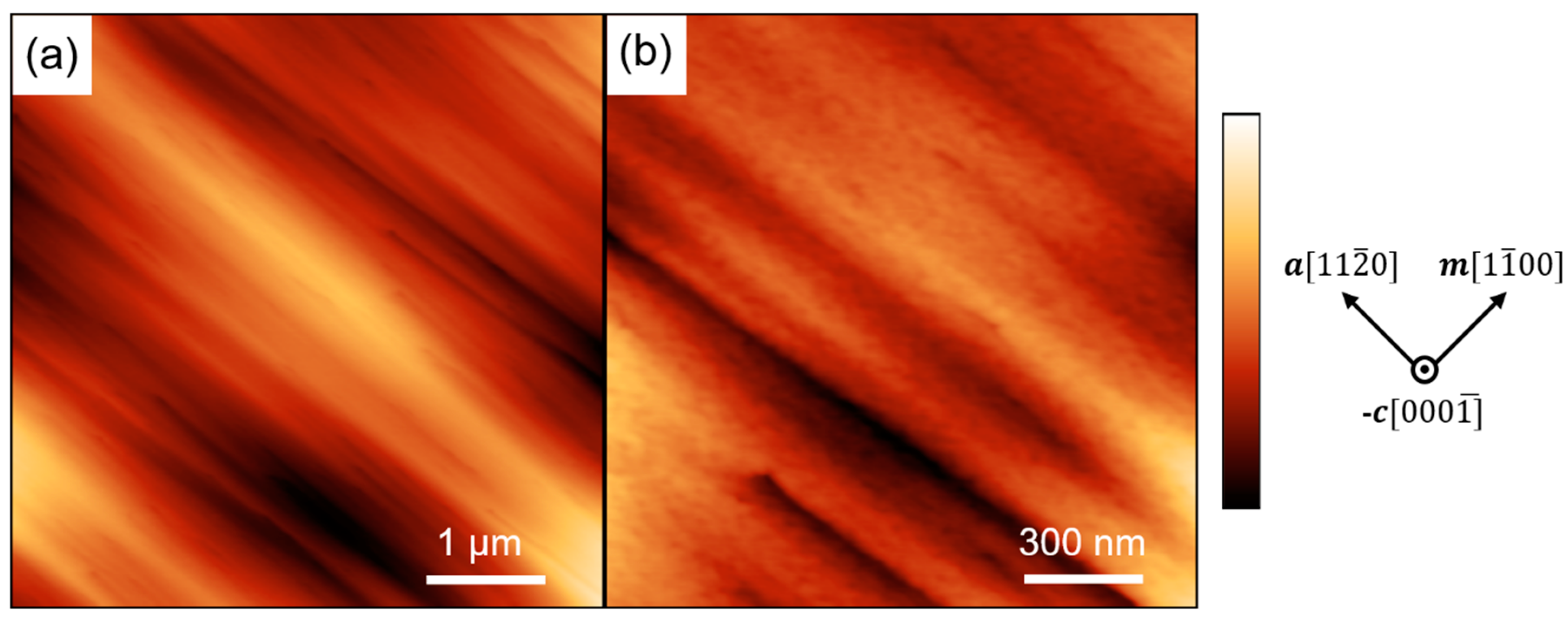
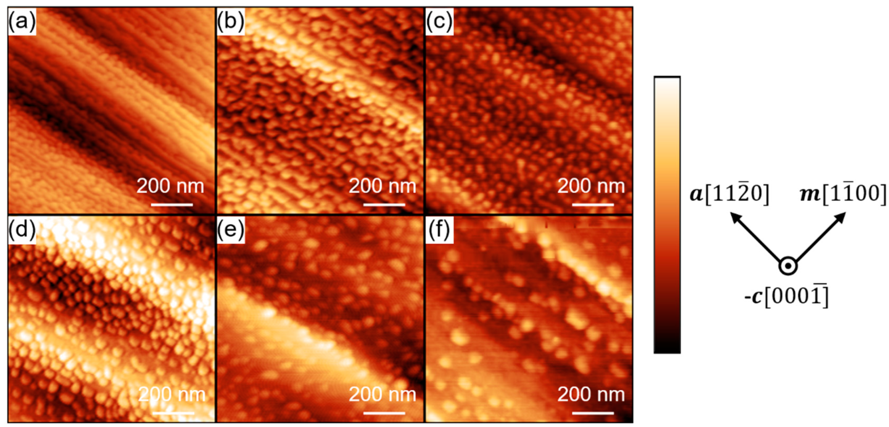
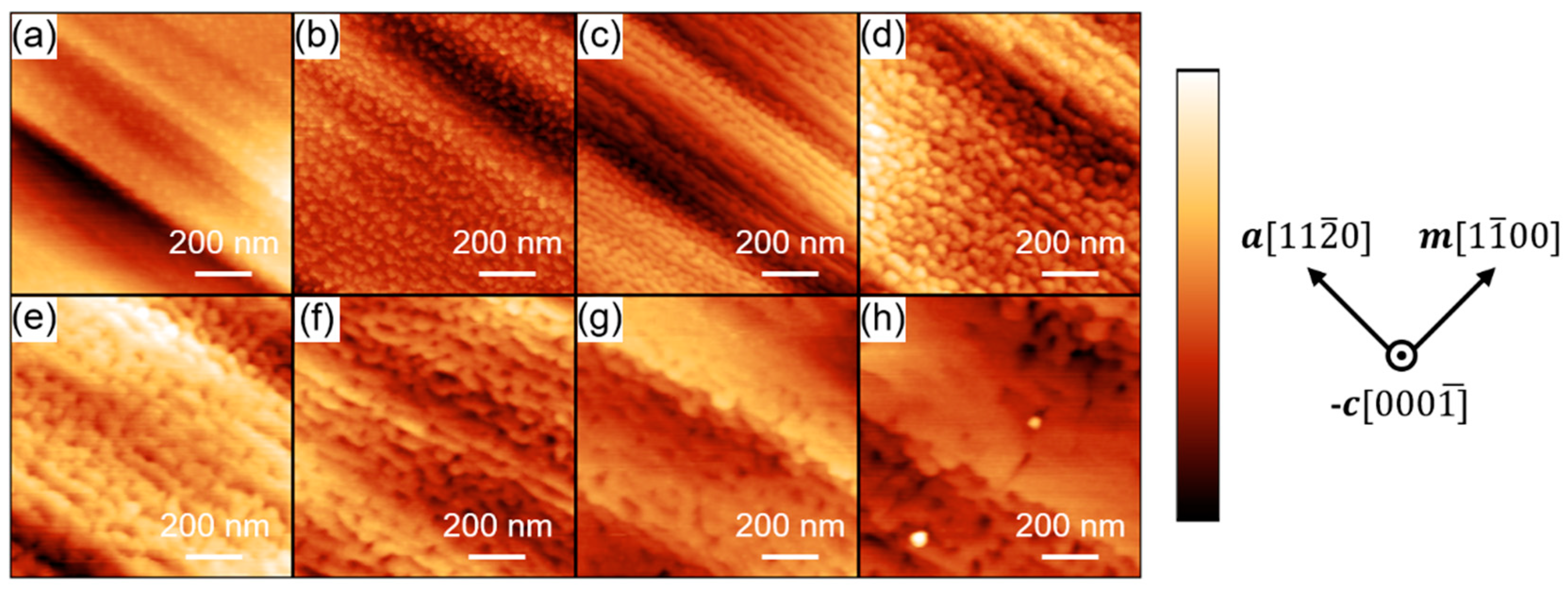
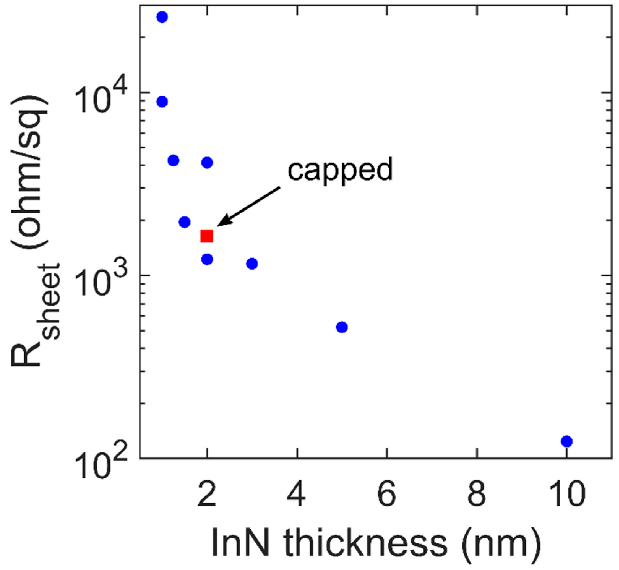
3. Results and Discussion

AFM imaging revealed insights into the optimal MOCVD growth conditions for InN quantum wire-like structure formations. Figure 2 shows the surface morphology of the N-polar GaN template layer for reference. Figure 3 depicts the surface morphologies of the samples from the InN growth temperature series. As the growth temperature increased, the InN dash structures became larger and less dense, which is expected thermodynamically and has been observed previously [44,48]. At the lowest temperature of 540 °C, the small, dense dashes merged along the a-direction of the surface steps to form wire segments, as seen in Figure 3a.
Figure 4 shows AFM images of samples from the InN thickness series grown at 540 °C. The InN transitioned from a dash-like morphology for thicknesses below 1 nm to a wire-like morphology for thicknesses of 1–2 nm. Figure 4c, which is the same as Figure 3a, shows the wire-like structures that were characteristic of N-polar InN growth at lower temperatures with relatively low thicknesses. The 2 nm thick sample, shown in Figure 4d, does show some wire segments, and it is possible that the more dash-like structures have formed on top of wire segments buried underneath. For InN thicknesses above 2 nm, the morphology became more film-like as the InN coalesced and fully covered the surface. The morphology results indicate that there is a narrow thickness window for the formation of N-polar InN wire-like structures rather than dashes or films.
The NH3 flow series resulted in no visible difference in InN wire-like surface morphology for all flows above 0.5 SLM NH3. For the sample with an NH3 flow of 0.5 SLM, indium droplets were present on the surface, indicating insufficient active nitrogen species on the growth surface due to the aforementioned reduced NH3 cracking efficiency at the low temperatures required for MOCVD InN growth. The results of the NH3 flow series suggest that the NH3 flow does not have a significant effect on InN quantum wire-like surface morphologies after a minimum lower limit of NH3 flow during growth to prevent In droplet formation. Considering the parameters of InN growth temperature, InN thickness, and NH3 flow during InN growth, it is clear that the growth temperature and thickness are the most important for facilitating InN wire segment formation rather than dashes or films. The low growth temperature ensures that the surface density of InN dashes is high enough to enable merging of dashes along the surface step direction, and limiting the InN thickness to 1–2 nm further allows dashes to merge without forming 2-D films.
While the AFM imaging of the InN surface morphologies visually indicated wire-like structures, the electrical measurements elucidated the extent of 1D electrical conduction in the wire-like samples and determined the practicality of such structures for electronic devices. Figure 5 shows the sheet resistances of fabricated InN samples extracted from TLM measurements. TLM measurements were taken along the direction of the wire segments (a) and perpendicular to the direction of the wire segments (m). The ratio of sheet resistance in the directions parallel and perpendicular to the wire segment direction indicated the onset of more 1D conduction—a ratio closer to one suggested more 2D conduction indicative of a quantum well, and a lower ratio suggested 1D conduction as the sheet resistance in the direction of the wire segments became much lower than the sheet resistance perpendicular to the wire segments. As depicted in Figure 5, the sheet resistance ratio significantly dropped below 1 for InN thicknesses of 2 nm and lower, confirming the observations of the surface morphology from the AFM images. The 1 nm thick InN sample was fully non-conductive perpendicular to the wire segment direction, suggesting a high extent of 1D conduction. The sheet resistances of truly wire-like samples with 1–1.5 nm InN ranged from 10—25 kΩ/□. While the measured TLM sheet resistances of the wire-like samples were in the kΩ/□ range, the thicker InN films were much less resistive. As seen in Figure 5, the 10 nm thick film sample had a TLM sheet resistance of 132 Ω/□. The measured Hall data of the 20 nm thick InN included a sheet carrier concentration of 1.1 × 1014 cm−2 and electron mobility of 397 cm2 V−1 s−1, giving a low sheet resistance of 142 Ω/□. Note that all samples with InN dashes rather than wire segments were resistive. These results indicated that thicker N-polar InN films grown by MOCVD had good quality and properties. The rather high sheet resistances measured for the InN wire-like samples likely originated from the required narrow InN thickness window to form 1D wire segments on the GaN template. As the InN must be only 1–2 nm thick for wire segment formation, dislocations forming at the InN/GaN interface were in close proximity to the wire segments, thereby amplifying the effects of electron scattering from the interfacial dislocations. It had been previously observed that the electron mobility in InN decreased for thin layers with decreasing layer thicknesses because of scattering by misfit dislocations forming at the InN/GaN interface [49]. In addition, InN wire segment thickness variations may affect the sheet resistance values. In order to reduce the sheet resistance of InN quantum wire segments, the interfacial dislocation density could be reduced by the growth of the InN on base layers with a lattice constant closer to that of InN, such as relaxed InGaN.
Figure 6 shows compiled sheet resistance data for all processed N-polar InN samples. A 2 nm thick InN wire-like sample that was capped with 6 nm of GaN grown at the InN growth temperature of 540 °C is indicated in the figure with an arrow. Samples capped with any thickness of GaN grown at a higher temperature than the InN were insulating. The sheet resistance of 2 nm thick N-polar InN wire segments increased from 1.2 kΩ/□ to 1.6 kΩ/□ with GaN cap layers grown at the InN growth temperature, indicating that electrical conduction could be retained with GaN capping, although it resulted in a slight increase in sheet resistance. The compiled electrical data warrant a discussion of the origin of electrical conduction in the N-polar InN wire segments. The electrical conduction could have possibly originated from the surface electron accumulation of InN or from unintentional oxygen impurity incorporation. It is known that N-polar III-nitride material grown by MOCVD typically exhibits higher impurity incorporation than metal-polar MOCVD-grown material [42], and the low growth temperature of InN also leads to higher impurity levels; thus, there could be high unintentional oxygen incorporation in the InN. The Hall and TLM data from the uncapped samples allowed for conduction in the bulk film and also via the surface electron accumulation layer, as the contacts were directly on the surface of the InN. However, the conductivity reduced only slightly with GaN capping, and it had been observed previously that capping InN layers with GaN eliminated the surface accumulation [50]. It was also possible that the electron accumulation concentration may have varied based on the volume of the InN layer, the varying polarity of InN surface on the wire segments, or both. Further investigation is required to fully clarify the mechanisms active in the InN wire segments.

4. Summary

In summary, MOCVD-grown horizontal N-polar InN quantum wire-like structures with 1D conduction were achieved on GaN using miscut sapphire substrates and tuning of the growth conditions. Growth temperatures on the lower end of the InN growth temperature window were found to have sufficient InN quantum dash densities, causing merging of the dashes along the direction of the surface steps, resulting in continuous wire segments. InN-formed dashes for thicknesses below 1 nm, wire segments for thicknesses between 1–2 nm, and continuous films for thicknesses above 2 nm. A minimum NH3 flow was required to prevent In droplet formation on the surface but, otherwise, did not have a significant effect on wire-like morphology. Fabricated InN wire samples exhibited sheet resistances between 10–26 kΩ/□, likely due to the close proximity of dislocations at the InN/GaN interface to the relatively thin wire segments. The sheet resistances in the wire segment direction were much lower than the sheet resistances perpendicular to the wire segment direction, suggesting anisotropic 1D conduction in the wire-like structures. An approach for future work could be the growth of InN on higher lattice constant underlayers such as relaxed InGaN, which would reduce the lattice mismatch between InN and its substrate, thereby reducing the interfacial threading dislocation density and possibly reducing the quantum wire segment sheet resistance.

Author Contributions

Conceptualization, V.R.M., S.P.D., U.K.M. and S.K.; methodology, V.R.M. and S.K.; formal analysis, V.R.M., W.L. (Wenjian Liu) and H.C.; investigation, V.R.M., W.L. (Wenjian Liu), H.C., W.L. (Weiyi Li) and R.H.; data curation, V.R.M. and S.K.; writing—original draft preparation, V.R.M.; writing—review and editing, V.R.M., W.L. (Wenjian Liu), H.C., W.L. (Weiyi Li), R.H., S.P.D., U.K.M. and S.K.; visualization, V.R.M.; supervision, S.P.D., U.K.M. and S.K.; project administration, S.P.D. and U.K.M.; funding acquisition, S.P.D. and U.K.M. All authors have read and agreed to the published version of the manuscript.

Funding

This work was supported by the Office of Naval Research (P. Maki) under Grant Reference No. N00014-21-1-2446. A portion of this work was performed using the MRL Shared Experimental Facilities, which were supported by the MRSEC Program of the NSF under Award No. DMR 1720256; a member of the NSF-funded Materials Research Facilities Network.

Data Availability Statement

The data that support the findings of this study are available from the corresponding author upon reasonable request.

Acknowledgments

A portion of this work was performed in the UCSB Nanofabrication Facility, an open access laboratory.

Conflicts of Interest

The authors declare no conflict of interest.

References

  1. Wu, Y.R.; Huang, C.Y.; Zhao, Y.; Speck, J.S. Nonpolar and semipolar LEDs. In Nitride Semiconductor Light-Emitting Diodes (LEDs): Materials, Technologies and Applications; Woodhead Publishing: Sawston, UK, 2013; pp. 250–275. [Google Scholar]
  2. Hwang, D.; Mughal, A.; Pynn, C.D.; Nakamura, S.; DenBaars, S.P. Sustained high external quantum efficiency in ultrasmall blue III-nitride micro-LEDs. Appl. Phys. Express 2017, 10, 032101. [Google Scholar] [CrossRef]
  3. Ponce, F.A.; Bour, D.P. Nitride-based semiconductors for blue and green light-emitting devices. Nature 1997, 386, 351–359. [Google Scholar] [CrossRef]
  4. Leonard, J.T.; Young, E.C.; Yonkee, B.P.; Cohen, D.A.; Margalith, T.; DenBaars, S.P.; Speck, J.S.; Nakamura, S. Demonstration of a III-nitride vertical-cavity surface-emitting laser with a III-nitride tunnel junction intracavity contact. Appl. Phys. Lett. 2015, 107, 091105. [Google Scholar] [CrossRef]
  5. Bhuiyan, A.G.; Hashimoto, A.; Yamamoto, A. Indium nitride (InN): A review on growth, characterization, and properties. J. Appl. Phys. 2003, 94, 2779–2808. [Google Scholar] [CrossRef]
  6. Polyakov, V.M.; Schwierz, F. Low-field electron mobility in wurtzite InN. Appl. Phys. Lett. 2006, 88, 032101. [Google Scholar] [CrossRef]
  7. Lu, H.; Schaff, W.J.; Eastman, L.F.; Stutz, C.E. Surface charge accumulation of InN films grown by molecular-beam epitaxy. Appl. Phys. Lett. 2003, 82, 1736–1738. [Google Scholar] [CrossRef]
  8. Tekcan, B.; Alkis, S.; Alevli, M.; Dietz, N.; Ortac, B.; Biyikli, N.; Okyay, A.K. A Near-Infrared Range Photodetector Based on Indium Nitride Nanocrystals Obtained Through Laser Ablation. IEEE Electron. Device Lett. 2014, 35, 936–938. [Google Scholar] [CrossRef]
  9. Lu, H.; Schaff, W.J.; Eastman, L.F. Surface chemical modification of InN for sensor applications. J. Appl. Phys. 2004, 96, 3577–3579. [Google Scholar] [CrossRef]
  10. Meissner, C.; Ploch, S.; Pristovsek, M.; Kneissl, M. Volmer-Weber growth mode of InN quantum dots on GaN by MOVPE. Phys. Status Solidi Curr. Top Solid State Phys. 2009, 6, S545–S548. [Google Scholar] [CrossRef]
  11. Lozano, J.G.; González, D.; Sánchez, A.M.; Araújo, D.; Ruffenach, S.; Briot, O.; García, R. Structural characterization of InN quantum dots grown by Metalorganic Vapour Phase Epitaxy. Phys. Status Solidi Curr. Top Solid State Phys. 2006, 3, 1687–1690. [Google Scholar] [CrossRef]
  12. Lozano, J.G.; Sánchez, A.M.; García, R.; Gonzalez, D.; Briot, O.; Ruffenach, S. Misfit relaxation of InN quantum dots: Effect of the GaN capping layer. Appl. Phys. Lett. 2006, 88, 151913. [Google Scholar] [CrossRef]
  13. Ambacher, O.; Brandt, M.S.; Dimitrov, R.; Metzger, T.; Stutzmann, M.; Fischer, R.A.; Miehr, A.; Bergmaier, A.; Dollinger, G. Thermal stability and desorption of group III nitrides prepared by metal organic chemical vapor deposition. J. Vac. Sci. Technol. B Microelectron. Nanom. Struct. 1996, 14, 3532–3542. [Google Scholar] [CrossRef]
  14. Benzarti, Z.; Sekrafi, T.; Khalfallah, A.; Bougrioua, Z.; Vignaud, D.; Evaristo, M.; Cavaleiro, A. Growth temperature effect on physical and mechanical properties of nitrogen rich InN epilayers. J. Alloys Compd. 2021, 885, 160951. [Google Scholar] [CrossRef]
  15. Liu, S.S.; Stevenson, D.A. Growth Kinetics and Catalytic Effects in the Vapor Phase Epitaxy of Gallium Nitride Growth Kinetics and Catalytic Effects in the Vapor Phase Epitaxy of Gallium Nitride. J. Electrochem. Soc. 1978, 125, 1161–1169. [Google Scholar] [CrossRef]
  16. Ogura, M. Growth and device applications of GaAs and InGaAs quantum wires on patterned substrates. J. Korean Phys. Soc. 2008, 53, 1442–1448. [Google Scholar] [CrossRef]
  17. Saito, H.; Nishi, K.; Ogura, I.; Sugou, S.; Sugimoto, Y. Room-Temperature Lasing Operation of a quantum-dot vertical-cavity surface-emitting laser. Appl. Phys. Lett. 1996, 69, 3140–3142. [Google Scholar] [CrossRef]
  18. Verma, J.; Kandaswamy, P.K.; Protasenko, V.; Verma, A.; Xing, H.G.; Jena, D. Tunnel-injection GaN quantum dot ultraviolet light-emitting diodes. Appl. Phys. Lett. 2013, 102, 041103. [Google Scholar] [CrossRef]
  19. Grandjean, N.; Ilegems, M. Visible InGaN/GaN Quantum-Dot Materials and Devices. Proc. IEEE 2007, 95, 1853–1865. [Google Scholar] [CrossRef]
  20. Fiore, A.; Oesterle, U.; Stanley, R.P.; Ilegems, M. High-efficiency light-emitting diodes at ≈1.3 μm using InAs-InGaAs quantum dots. IEEE Photonics Technol. Lett. 2000, 12, 1601–1603. [Google Scholar] [CrossRef]
  21. Widmann, F.; Daudin, B.; Feuillet, G.; Samson, Y.; Rouvière, J.L.; Pelekanos, N. Growth kinetics and optical properties of self-organized GaN quantum dots. J. Appl. Phys. 1998, 83, 7618–7624. [Google Scholar] [CrossRef]
  22. Coleman, J.J.; Young, J.D.; Garg, A. Semiconductor quantum dot lasers: A tutorial. J. Light Technol. 2011, 29, 499–510. [Google Scholar] [CrossRef]
  23. Ruffenach, S.; Maleyre, B.; Briot, O.; Gil, B. Growth of InN quantum dots by MOVPE. Phys. Status Solidi C Conf. 2005, 2, 826–832. [Google Scholar] [CrossRef]
  24. Reilly, C.E.; Lund, C.; Nakamura, S.; Mishra, U.K.; Denbaars, S.P.; Keller, S. Infrared luminescence from N-polar InN quantum dots and thin films grown by metal organic chemical vapor deposition. Appl. Phys. Lett. 2019, 114, 241103. [Google Scholar] [CrossRef]
  25. Ke, W.C.; Fu, C.P.; Chen, C.Y.; Lee, L.; Ku, C.S.; Chou, W.C.; Chang, W.-H.; Lee, M.C.; Chen, W.K.; Lin, W.J.; et al. Photoluminescence properties of self-assembled InN dots embedded in GaN grown by metal organic vapor phase epitaxy. Appl. Phys. Lett. 2006, 88, 10–13. [Google Scholar] [CrossRef]
  26. Werner, F.; Limbach, F.; Carsten, M.; Denker, C.; Malindretos, J.; Rizzi, A. Electrical conductivity of InN nanowires and the influence of the native indium oxide formed at their surface. Nano Lett. 2009, 9, 1567–1571. [Google Scholar] [CrossRef]
  27. Chang, Y.L.; Li, F.; Fatehi, A.; Mi, Z. Molecular beam epitaxial growth and characterization of non-tapered InN nanowires on Si(111). Nanotechnology 2009, 20, 345203. [Google Scholar] [CrossRef]
  28. Chao, C.K.; Chyi, J.-I.; Hsiao, C.N.; Kei, C.C.; Kuo, S.Y.; Chang, H.-S.; Hsu, T.M. Catalyst-free growth of indium nitride nanorods by chemical-beam epitaxy. Appl. Phys. Lett. 2006, 88, 2004–2007. [Google Scholar] [CrossRef]
  29. Stoica, T.; Meijers, R.; Calarco, R.; Richter, T.; Lüth, H. MBE growth optimization of InN nanowires. J. Cryst. Growth 2006, 290, 241–247. [Google Scholar] [CrossRef]
  30. Tang, T.; Han, S.; Jin, W.; Liu, X.; Li, C.; Zhang, D.; Zhou, C.; Chen, B.; Han, J.; Meyyapan, M. Synthesis and characterization of single-crystal indium nitride nanowires. J. Mater. Res. 2004, 19, 423–426. [Google Scholar] [CrossRef]
  31. Zhao, S.; Fathololoumi, S.; Bevan, K.H.; Liu, D.P.; Kibria, M.G.; Li, Q.; Wang, G.T.; Guo, H.; Mi, Z. Tuning the Surface Charge Properties of Epitaxial InN Nanowires. Nano Lett. 2012, 12, 2877–2882. [Google Scholar] [CrossRef]
  32. Cheng, G.; Stern, E.; Turner-Evans, D.; Reed, M.A. Electronic properties of InN nanowires. Appl. Phys. Express 2005, 87, 253103. [Google Scholar] [CrossRef]
  33. Zhao, S.; Salehzadeh, O.; Alagha, S.; Kavanagh, K.L.; Watkins, S.P.; Mi, Z. Probing the electrical transport properties of intrinsic InN nanowires. Appl. Phys. Lett. 2013, 102, 073102. [Google Scholar] [CrossRef]
  34. Parry, H.J.; Ashwin, M.J.; Neave, J.H.; Jones, T.S. Growth of InAs/InP (001) nanostructures: The transition from quantum wires to quantum dots. J. Cryst. Growth 2005, 278, 131–135. [Google Scholar] [CrossRef]
  35. Takasuka, Y.; Yonei, K.; Yamauchi, H.; Ogura, M. InGaAs/AlGaAs Quantum Wire DFB Buried HeteroStructure Laser Diode by One-Time Selective MOCVD on Ridge Substrate. Jpn. J. Appl. Phys. 2005, 44, 2546. [Google Scholar] [CrossRef]
  36. Nakashima, H.; Takeuchi, M.; Inoue, K.; Takeuchi, T.; Inoue, Y.; Fischer, P.; Christen, J.; Grundmann, M.; Bimberg, D. Size-dependent luminescence of GaAs quantum wires on vicinal GaAs (110) surfaces with giant steps formed by MBE. Phys. B 1996, 227, 291–294. [Google Scholar] [CrossRef]
  37. Notzel, R.; Ledentsov, N.N.; Daweritz, L.; Ploog, K.; Hohenstein, M. Semiconductor quantum-wire structures directly grown on high-index surfaces. Phys. Rev. B 1992, 45, 3507–3515. [Google Scholar] [CrossRef]
  38. Keller, S.; Pfaff, N.; DenBaars, S.P.; Mishra, U.K. Polarization spectroscopy of N-polar AlGaN/GaN multi quantum wells grown on vicinal (000-1) GaN. Appl. Phys. Lett. 2012, 101, 182103. [Google Scholar] [CrossRef]
  39. Renard, J.; Amstatt, B.; Bougerol, C.; Bellet-Amalric, E.; Daudin, B.; Gayral, B. Optical properties of m -plane GaN quantum dots and quantum wires. J. Appl. Phys. 2008, 104, 1–5. [Google Scholar] [CrossRef]
  40. Nath, D.N.; Park, P.S.; Esposto, M.; Brown, D.; Keller, S.; Mishra, U.K.; Rajan, S. Polarization engineered 1-dimensional electron gas arrays. J. Appl. Phys. 2012, 111, 043715. [Google Scholar] [CrossRef]
  41. Nath, D.N.; Keller, S.; Hsieh, E.; Denbaars, S.P.; Mishra, U.K.; Rajan, S. Lateral confinement of electrons in vicinal N-polar AlGaN/GaN heterostructure. Appl. Phys. Lett. 2010, 97, 162106. [Google Scholar] [CrossRef]
  42. Keller, S.; Li, H.; Laurent, M.; Hu, Y.; Pfaff, N.; Lu, J.; Brown, D.F.; Fichtenbaum, N.A.; Speck, J.S.; DenBaars, S.P. Recent progress in metal-organic chemical vapor deposition of (0001¯) N-polar group-III nitrides. Semicond. Sci. Technol. 2014, 29, 113001. [Google Scholar] [CrossRef]
  43. Keller, S.; Fichtenbaum, N.A.; Wu, F.; Brown, D.B.; Rosales, A.M.; DenBaars, S.P.; Speck, J.S.; Mishra, U.K. Influence of the substrate misorientation on the properties of N-polar GaN films grown by metal organic chemical vapor deposition. J. Appl. Phys. 2007, 102, 083546. [Google Scholar] [CrossRef]
  44. Reilly, C.E.; Nakamura, S.; DenBaars, S.P.; Keller, S. MOCVD Growth and Characterization of InN Quantum Dots. Phys. Status Solidi Basic Res. 2019, 257, 1900508. [Google Scholar] [CrossRef]
  45. Lund, C.; Catalano, M.; Wang, L.; Wurm, C.; Mates, T.; Kim, M.; Nakamura, S.; Denbaars, S.; Mishra, U.K.; Keller, S. Metal-organic chemical vapor deposition of N-polar InN quantum dots and thin films on vicinal GaN. J. Appl. Phys. 2018, 123, 055702. [Google Scholar] [CrossRef]
  46. Romanczyk, B.; Wienecke, S.; Guidry, M.; Li, H.; Ahmadi, E.; Zheng, X.; Keller, S.; Mishra, U.K. Demonstration of Constant 8 W / mm Power Density at 10, 30, and 94 GHz in State-of-the-Art Millimeter-Wave N-polar GaN MISHEMTs. IEEE Trans. Electron Devices 2018, 65, 45–50. [Google Scholar] [CrossRef]
  47. Rajan, S.; Chini, A.; Wong, M.H.; Speck, J.S.; Mishra, U.K. N-polar GaNAlGaNGaN high electron mobility transistors. J. Appl. Phys. 2007, 102, 044501. [Google Scholar] [CrossRef]
  48. Briot, O.; Maleyre, B.; Ruffenach, S. Indium nitride quantum dots grown by metalorganic vapor phase epitaxy. Appl. Phys. Lett. 2003, 83, 2919–2921. [Google Scholar] [CrossRef]
  49. Lebedev, V.; Cimalla, V.; Baumann, T.; Ambacher, O.; Morales, F.M.; Lozano, J.G.; Gonzalez, D. Effect of dislocations on electrical and electron transport properties of InN thin films. II. Density and mobility of the carriers. J. Appl. Phys. 2006, 100, 094903. [Google Scholar] [CrossRef]
  50. Liu, W.; Tan, R.J.N.; Soh, C.B.; Chua, S.J. The effects of cap layers on electrical properties of indium nitride films. Appl. Phys. Lett. 2010, 97, 042110. [Google Scholar] [CrossRef]
Figure 1. Epitaxial structure of uncapped N−polar InN samples.
Crystals 13 00699 g001
Figure 2. AFM images of N−polar semi−insulating GaN template with surface steps parallel to the GaN a−direction. (a) 5 × 5 μm. (b) 1.5 × 1.5 μm. Scale bar shown at right is 0–50 nm for (a) and 0–15 nm for (b).
Crystals 13 00699 g002
Figure 3. 1 × 1 µm AFM images of nominally 1 nm of N−polar InN grown at different temperatures. InN dash and wire−like structures are aligned along the a−direction. (a) 540 °C. (b) 560 °C. (c) 580 °C. (d) 600 °C. (e) 620 °C. (f) 640 °C. Vertical scale bar is 0–20 nm for (a) and 0–10 nm for (bf).
Crystals 13 00699 g003
Figure 4. 1 × 1 µm AFM images of N−polar InN grown at 540 °C with different thicknesses. InN dash and wire−like structures are aligned along the a−direction. (a) 0.25 nm. (b) 0.5 nm. (c) 1 nm. (d) 2 nm. (e) 3 nm. (f) 5 nm. (g) 10 nm. (h) 20 nm. Vertical scale bar is 0–20 nm for (a,c,g,h) and 0–10 nm for (b,df).
Crystals 13 00699 g004
Figure 5. DC TLM data for processed samples from the N-polar InN thickness series. The blue curve indicates the sheet resistance parallel to the wire segment direction. The red curve indicates the ratio of sheet resistance parallel to the wire segment direction and sheet resistance perpendicular to the wire segment direction.
Crystals 13 00699 g005
Figure 6. Combined sheet resistance data for processed N-polar InN samples along the a-direction. The red square indicates an InN wire-like sample capped with 6 nm of GaN. The equivalent uncapped sample is the blue circle just below it.
Crystals 13 00699 g006
Disclaimer/Publisher’s Note: The statements, opinions and data contained in all publications are solely those of the individual author(s) and contributor(s) and not of MDPI and/or the editor(s). MDPI and/or the editor(s) disclaim responsibility for any injury to people or property resulting from any ideas, methods, instructions or products referred to in the content.

