

Studying the Thermoelastic Waves Induced by Pulsed Lasers Due to the Interaction between Electrons and Holes on Semiconductor Materials under the Hall Current Effect

Abstract
:1. Introduction
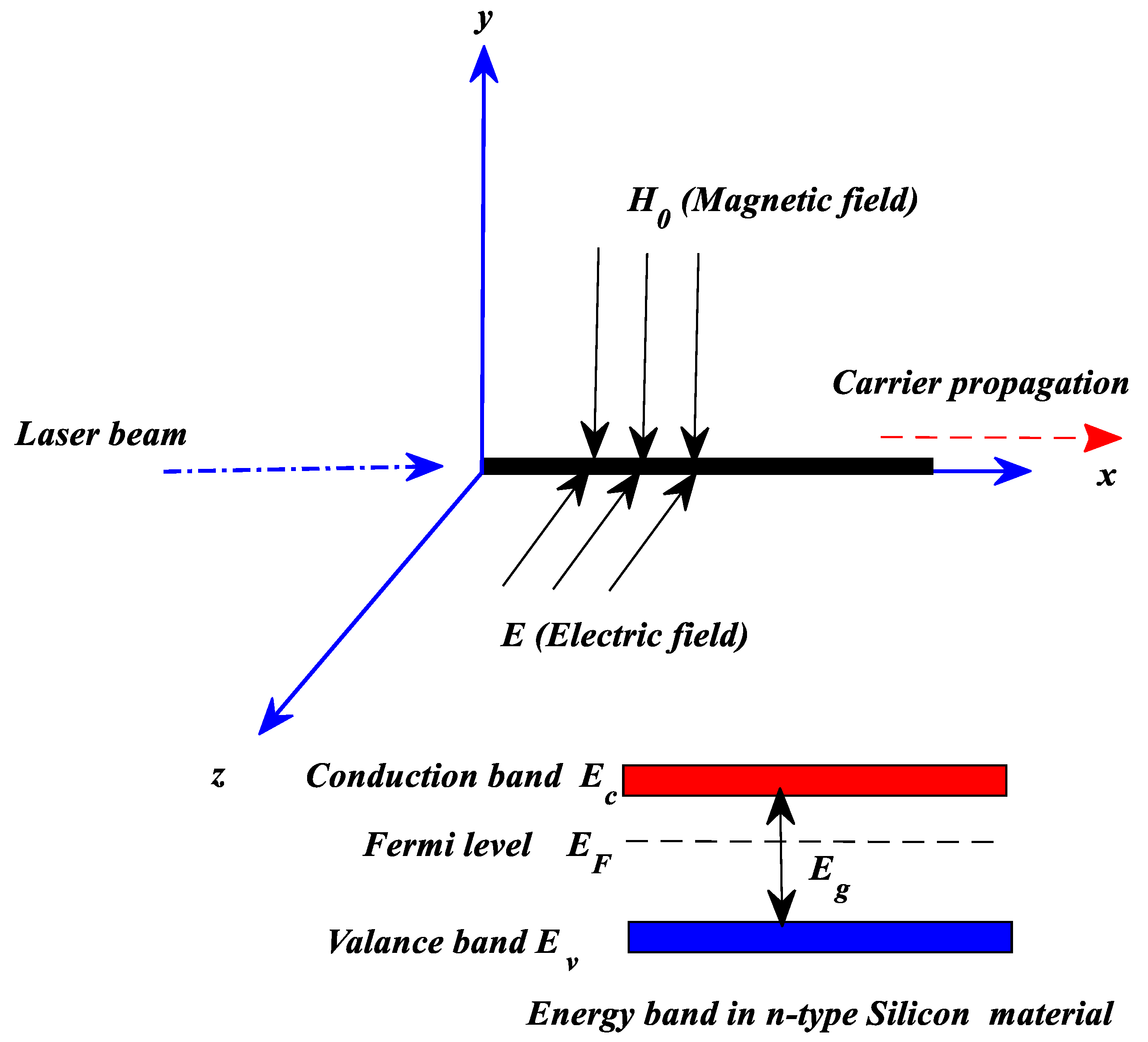
2. Basic Equations
3. The Mathematical Analysis
4. Boundary Conditions
5. Inversion of the Laplace Transform
6. Validation
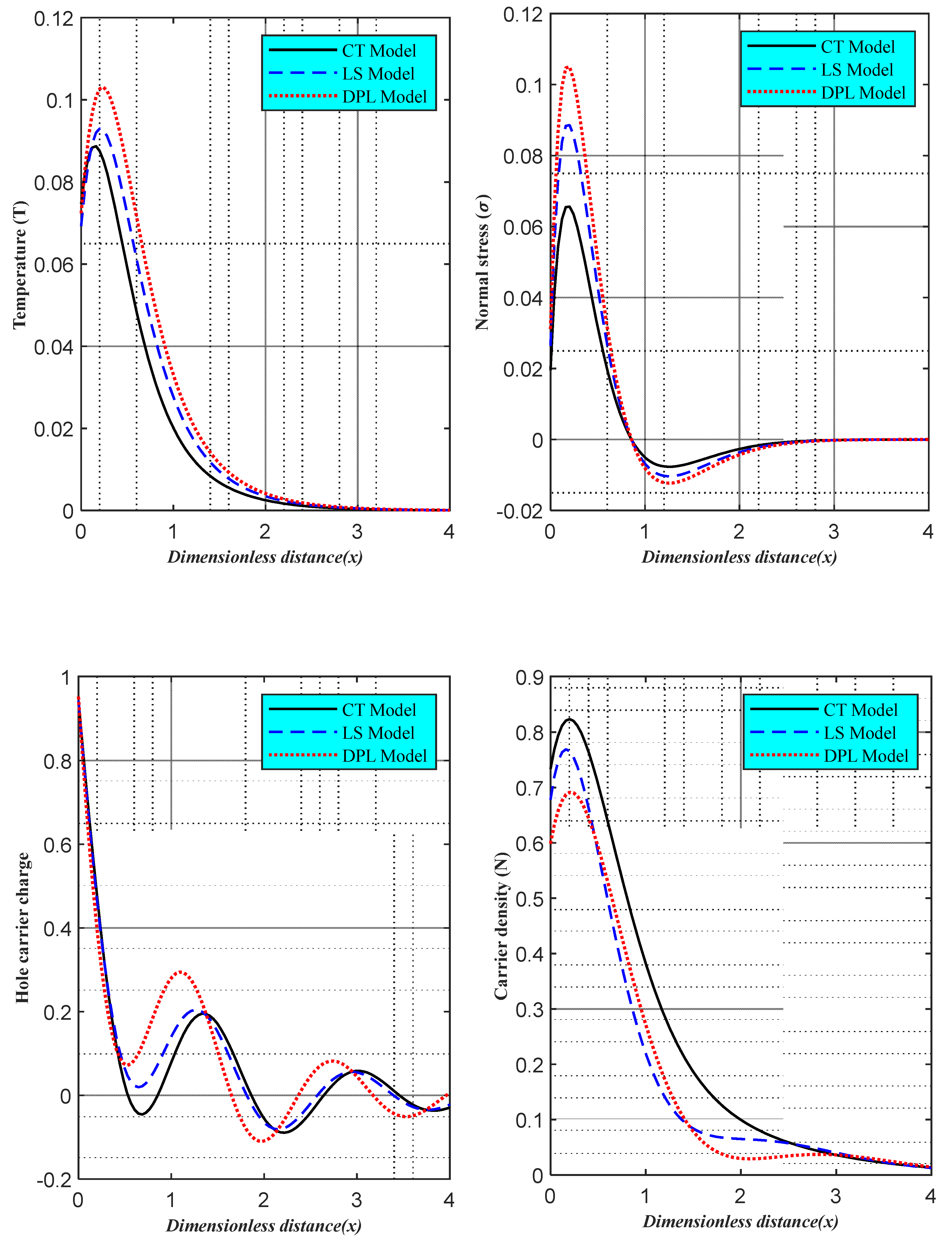
6.1. The Photo-Thermoelasticity Models
- (1)
- ; this yields the dual phase lag (DPL) model.
- (2)
- , ; this yields the Lord and Șhulman (LS) model.
- (3)
- ; this yields the coupled thermoelasticity (CT) model.
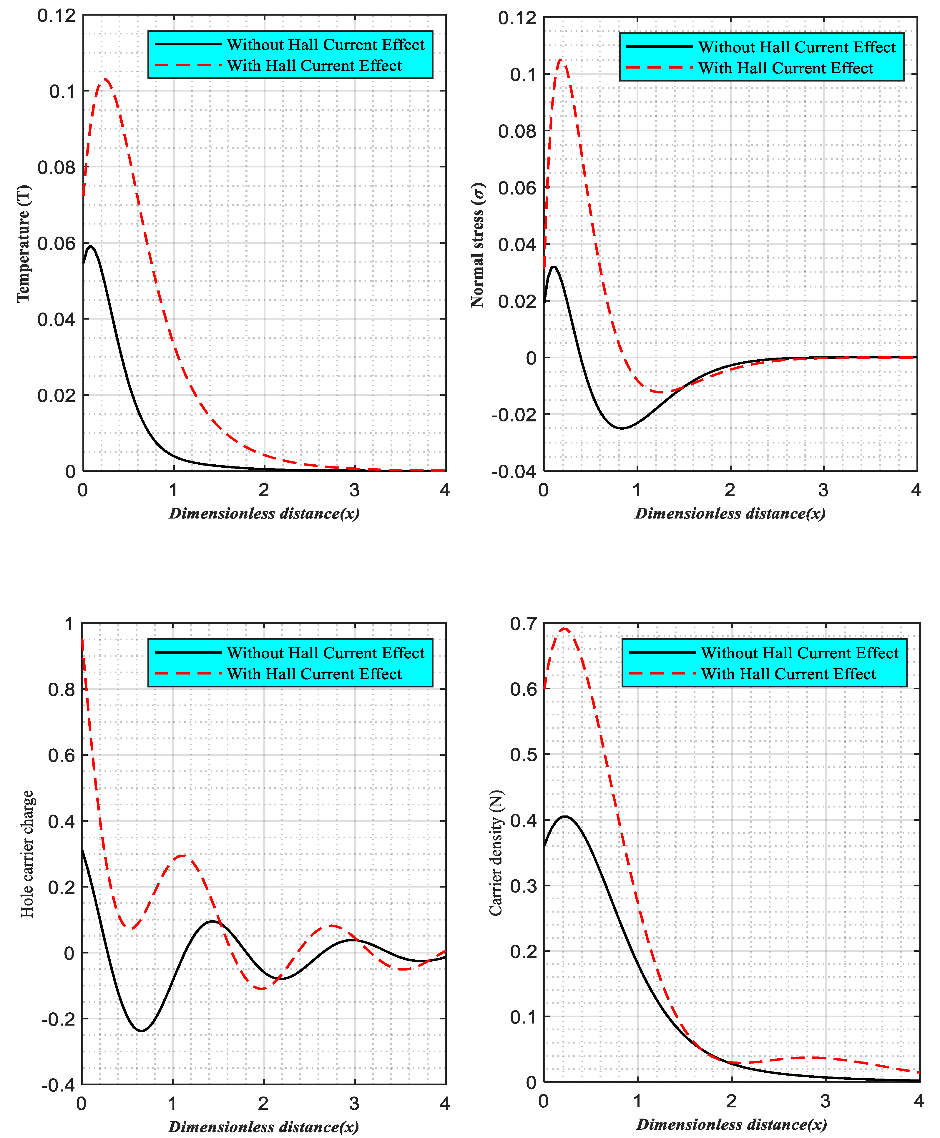
6.2. Effect of Magnetic Field
6.3. Without Electron-Hole Interaction, Thermoelasticity Theory
6.4. The Magneto-Photo-Thermoelasticity Theory
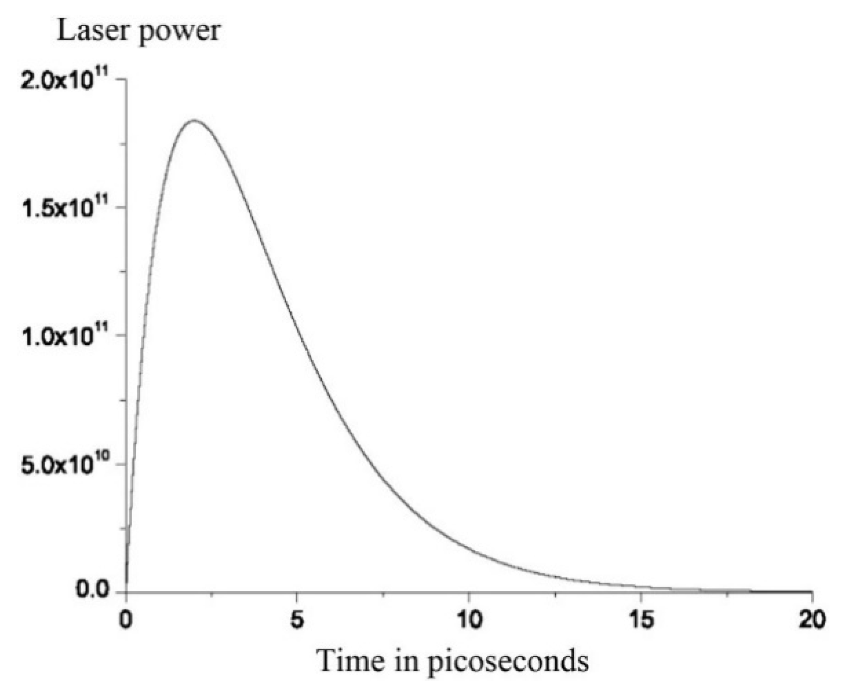
6.5. The Non-Gaussian Laser Pulses Impact
7. Numerical Results and Discussions
7.1. The Photo-Electronic-Thermoelasticity Models
7.2. The Impact of Hall’s Current
7.3. The Laser Pulses Effect
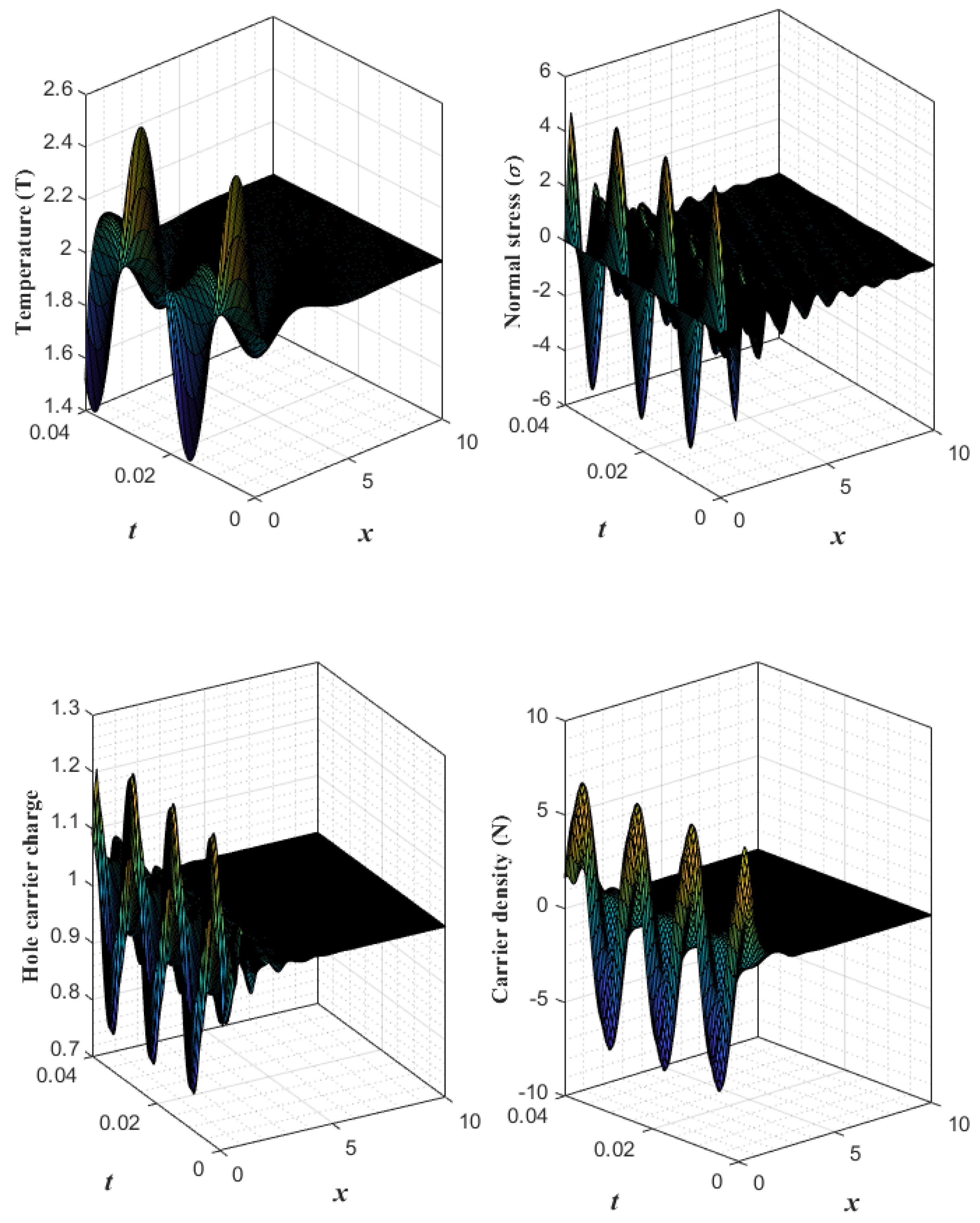
7.4. The 3D Graph
8. Conclusions
Author Contributions
Funding
Data Availability Statement
Acknowledgments
Conflicts of Interest
Nomenclature
| Lame’s constants, | |
| Electrons concentration | |
| Holes concentration | |
| Absolute temperature | |
| The volume coefficient of thermal expansion | |
| Stress tensor | |
| Density | |
| Thermo-diffusive parameters of Electrons and Holes | |
| The thermal and elastic relaxation times | |
| The holes and electron’s relaxation times | |
| The linear thermal expansion coefficient | |
| Specific heat | |
| Thermal conductivity | |
| The photo-generated carrier lifetime | |
| The energy gap | |
| The electron’s elasto-diffusive parameter | |
| The holes elasto-diffusive parameter | |
| The coefficients of electronic deformation | |
| The coefficient of holes deformation | |
| Peltier-Dufour- Seebeck-Soret-like constants | |
| The diffusion coefficient of the electrons and holes | |
| The flux-like constants |
References
- Hall, E. On a New Action of the Magnet on Electric Currents. Am. J. Math. 1879, 2, 287–292. [Google Scholar] [CrossRef]
- Klitzing, K.; Dorda, G.; Pepper, M. New Method for High-Accuracy Determination of the Fine-Structure Constant Based on Quantized Hall Resistance. Phys. Rev. Lett. 1980, 45, 494–497. [Google Scholar] [CrossRef] [Green Version]
- Mendez, E.; Esaki, L.; Chang, L. Quantum Hall Effect in a Two-Dimensional Electron-Hole Gas. Phys. Rev. Lett. 1985, 55, 2216–2219. [Google Scholar] [CrossRef] [PubMed]
- Büttiker, M. Absence of backscattering in the quantum Hall effect in multiprobe conductors. Phys. Rev. B 1988, 38, 9375–9389. [Google Scholar] [CrossRef]
- Takashina, K.; Nicholas, R.J.; Kardynal, B.; Mason, N.J.; Maude, D.K.; Portal, J.C. Breakdown of the quantum Hall effect in an electron–hole system. Phys. B Condens. Matter 2001, 298, 8–12. [Google Scholar] [CrossRef]
- Biot, M.A. Thermoelasticity and irreversible thermodynamics. J. Appl. Phys. 1956, 27, 240–253. [Google Scholar] [CrossRef]
- Lord, H.; Shulman, Y. A generalized dynamical theory of Thermoelasticity. J. Mech. Phys. Solids 1967, 15, 299–309. [Google Scholar] [CrossRef]
- Green, A.E.; Lindsay, K.A. Thermoelasticity. J. Elast. 1972, 2, 1–7. [Google Scholar] [CrossRef]
- Chandrasekharaiah, D.S. Thermoelasticity with second sound: A review. Appl. Mech. Rev. 1986, 39, 355–376. [Google Scholar] [CrossRef]
- Chandrasekharaiah, D.S. Hyperbolic Thermoelasticity: A review of recent literature. Appl. Mech. Rev. 1998, 51, 705–729. [Google Scholar] [CrossRef]
- Sharma, J.N.; Kumar, V.; Dayal, C. Reflection of generalized thermoelastic waves from the boundary of a half-space. J. Therm. Stress. 2003, 26, 925–942. [Google Scholar] [CrossRef]
- Lotfy, K.; Abo-Dahab, S. Two-dimensional problem of two temperature generalized thermoelasticity with normal mode analysis under thermal shock problem. J. Comput. Theor. Nanosci. 2015, 12, 1709–1719. [Google Scholar] [CrossRef]
- Othman, M.; Lotfy, K. The influence of gravity on 2-D problem of two temperature generalized thermoelastic medium with thermal relaxation. J. Comput. Theor. Nanosci. 2015, 12, 2587–2600. [Google Scholar] [CrossRef]
- Maruszewski, B. Electro-magneto-thermo-elasticity of Extrinsic Semiconductors, Classical Irreversible Thermodynamic Approach. Arch. Mech. 1986, 38, 71–82. [Google Scholar]
- Maruszewski, B. Electro-magneto-thermo-elasticity of Extrinsic Semiconductors, Extended Irreversible Thermodynamic Approach. Arch. Mech. 1986, 38, 83–95. [Google Scholar]
- Maruszewski, B. Coupled Evolution Equations of Deformable Semiconductors. Int. J. Eng. Sci. 1987, 25, 145–153. [Google Scholar] [CrossRef]
- Sharma, J.; Thakur, N. Plane harmonic elasto-thermodiffusive waves in semiconductor materials. J. Mech. Mater. Struct. 2006, 1, 813–835. [Google Scholar] [CrossRef] [Green Version]
- Mandelis, A. Photoacoustic and Thermal Wave Phenomena in Semiconductors; Elsevier: Alpharetta, GA, USA, 1987. [Google Scholar]
- Almond, D.; Patel, P. Photothermal Science and Techniques; Springer Science & Business Media: Berlin, Germany, 1996. [Google Scholar]
- Gordon, J.P.; Leite, R.C.C.; Moore, R.S.; Porto, S.P.S.; Whinnery, J.R. Long-transient effects in lasers with inserted liquid samples. Bull. Am. Phys. Soc. 1964, 119, 501. [Google Scholar] [CrossRef]
- Lotfy, K. Effect of variable thermal conductivity during the photothermal diffusion process of semiconductor medium. Silicon 2019, 11, 1863–1873. [Google Scholar] [CrossRef]
- Lotfy, K.; Tantawi, R.S. Photo-thermal-elastic interaction in a functionally graded material (FGM) and magnetic field. Silicon 2020, 12, 295–303. [Google Scholar] [CrossRef]
- Lotfy, K. A novel model of magneto photothermal diffusion (MPD) on polymer nano-composite semiconductor with initial stress. Waves Ran. Comp. Med. 2021, 31, 83–100. [Google Scholar] [CrossRef]
- Lotfy, K.; El-Bary, A.; Hassan, W.; Ahmed, M. Hall current influence of microtemperature magneto-elastic semiconductor material. Superlattices Microstruct. 2020, 139, 106428. [Google Scholar] [CrossRef]
- Mahdy, A.; Lotfy, K.; Ahmed, M.; El-Bary, A.; Ismail, E. Electromagnetic Hall current effect and fractional heat order for microtemperature photo-excited semiconductor medium with laser pulses. Results Phys. 2020, 17, 103161. [Google Scholar] [CrossRef]
- Mahdy, A.; Lotfy, K.; El-Bary, A.; Tayel, I. Variable thermal conductivity and hyperbolic two-temperature theory during magneto-photothermal theory of semiconductor induced by laser pulses. Eur. Phys. J. Plus 2021, 136, 651. [Google Scholar] [CrossRef]
- Lotfy, K. The elastic wave motions for a photothermal medium of a dual-phase-lag model with an internal heat source and gravitational field. Can. J. Phys. 2016, 94, 400–409. [Google Scholar] [CrossRef] [Green Version]
- Lotfy, K. A Novel Model of Photothermal Diffusion (PTD) fo Polymer Nano- composite Semiconducting of Thin Circular Plate. Phys. B Condens. Matter 2018, 537, 320–328. [Google Scholar] [CrossRef]
- Lotfy, K.; Kumar, R.; Hassan, W.; Gabr, M. Thermomagnetic effect with microtemperature in a semiconducting Photothermal excitation medium. Appl. Math. Mech. Engl. Ed. 2018, 39, 783–796. [Google Scholar] [CrossRef]
- Mahdy, A.; Lotfy, K.; El-Bary, A.; Sarhan, H. Effect of rotation and magnetic field on a numerical-refined heat conduction in a semiconductor medium during photo-excitation processes. Eur. Phys. J. Plus 2021, 136, 553. [Google Scholar] [CrossRef]
- Lotfy, K. A novel model for Photothermal excitation of variable thermal conductivity semiconductor elastic medium subjected to mechanical ramp type with two-temperature theory and magnetic field. Sci. Rep. 2019, 9, 3319. [Google Scholar] [CrossRef]
- Marin, M. On existence and uniqueness in thermoelasticity of micropolar bodies. Comptes Rendus Acad. Sci. Ser. II Fasc. B 1995, 321, 375–480. [Google Scholar]
- Marin, M.; Marinescu, C. Thermoelasticity of initially stressed bodies, Asymptotic equipartition of energies. Int. J. Eng. Sci. 1998, 36, 73–86. [Google Scholar] [CrossRef]
- Alzahrani, F.; Hobiny, A.; Abbas, I.; Marin, M. An eigenvalues approach for a two-dimensional porous medium based upon weak, normal and strong thermal conductivities. Symmetry 2020, 12, 848. [Google Scholar] [CrossRef]
- Scutaru, M.; Vlase, S.; Marin, M.; Modrea, A. New analytical method based on dynamic response of planar mechanical elastic systems. Bound. Value Probl. 2020, 2020, 104. [Google Scholar] [CrossRef]
- Marin, M.; Ellahi, R.; Vlase, S.; Bhatti, M. On the decay of exponential type for the solutions in a dipolar elastic body. J. Taibah Univ. Sci. 2020, 14, 534–540. [Google Scholar] [CrossRef] [Green Version]
- Singh, A.; Das, S.; Altenbach, H.; Craciun, E.-M. Semi-infinite moving crack in an orthotropic strip sandwiched between two identical half planes. ZAMM Z. Angew. Math. Mech. 2020, 100, e201900202. [Google Scholar] [CrossRef]
- Mondal, S.; Sur, A. Photo-thermo-elastic wave propagation in anorthotropic semiconductor with a spherical cavity and memory responses. Waves Random Complex Media 2021, 31, 1835–1858. [Google Scholar] [CrossRef]
- Abbas, I.; Alzahranib, F.; Elaiwb, A. A DPL model of photothermal interaction in a semiconductor material. Waves Random Complex Media 2019, 29, 328–343. [Google Scholar] [CrossRef]
- Brancik, L. Programs for fast numerical inversion of Laplace transforms in MATLAB language environment. In Proceedings of the 7th Conference MATLAB, Prague, Czech Republic; 1999; Volume 99, pp. 27–39. [Google Scholar]
- Xiao, Y.; Shen, C.; Zhang, W. Screening and prediction of metal-doped α-borophene monolayer for nitric oxide elimination. Mater. Today Chem. 2022, 25, 100958. [Google Scholar] [CrossRef]
- Liu, J.; Han, M.; Wang, R.; Xu, S.; Wang, X. Photothermal phenomenon: Extended ideas for thermophysical properties characterization. J. Appl. Phys. 2022, 131, 065107. [Google Scholar] [CrossRef]


| Unit | Symbol | Value |
|---|---|---|
Disclaimer/Publisher’s Note: The statements, opinions and data contained in all publications are solely those of the individual author(s) and contributor(s) and not of MDPI and/or the editor(s). MDPI and/or the editor(s) disclaim responsibility for any injury to people or property resulting from any ideas, methods, instructions or products referred to in the content. |
© 2023 by the authors. Licensee MDPI, Basel, Switzerland. This article is an open access article distributed under the terms and conditions of the Creative Commons Attribution (CC BY) license (https://creativecommons.org/licenses/by/4.0/).
Share and Cite
Becheikh, N.; Ghazouani, N.; El-Bary, A.A.; Lotfy, K. Studying the Thermoelastic Waves Induced by Pulsed Lasers Due to the Interaction between Electrons and Holes on Semiconductor Materials under the Hall Current Effect. Crystals 2023, 13, 665. https://doi.org/10.3390/cryst13040665
Becheikh N, Ghazouani N, El-Bary AA, Lotfy K. Studying the Thermoelastic Waves Induced by Pulsed Lasers Due to the Interaction between Electrons and Holes on Semiconductor Materials under the Hall Current Effect. Crystals. 2023; 13(4):665. https://doi.org/10.3390/cryst13040665
Chicago/Turabian StyleBecheikh, Nidhal, Nejib Ghazouani, Alaa A. El-Bary, and Khaled Lotfy. 2023. "Studying the Thermoelastic Waves Induced by Pulsed Lasers Due to the Interaction between Electrons and Holes on Semiconductor Materials under the Hall Current Effect" Crystals 13, no. 4: 665. https://doi.org/10.3390/cryst13040665