Article

Effect of Substrate Temperature on Variations in the Structural and Optical Properties of Cu2O Thin Films Deposited via RF Magnetron Sputtering

1
Department of Materials Science and Engineering, Pusan National University, Busan 46241, Republic of Korea
2
Department of Mechatronics Convergence, Changwon National University, Changwon 51140, Republic of Korea
3
Division of Materials Science and Engineering, Silla University, Busan 46958, Republic of Korea
*
Authors to whom correspondence should be addressed.
Crystals 2023, 13(4), 643; https://doi.org/10.3390/cryst13040643
Submission received: 25 February 2023 / Revised: 5 April 2023 / Accepted: 5 April 2023 / Published: 9 April 2023
(This article belongs to the Special Issue Feature Paper in "Materials for Energy Applications" 2022–2023)

Abstract

:
In the present study, Cu2O films were deposited on a glass substrate via RF (radio frequency) magnetron sputtering under substrate temperature conditions that ranged from room temperature (RT, 25 °C) to 400 °C. The structural, compositional, and optical properties of the Cu2O films were analyzed in relation to the experimental variables by applying various measurement methods. The substrate temperature was a crucial factor in shaping the structural, compositional, and optical properties of the Cu2O films that were synthesized via RF-magnetron sputtering. Our findings revealed that the Cu2O films exhibited a cubic structure, which was confirmed by XRD analysis. Specifically, the (111) and (200) planes showed different trends with respect to the substrate temperature. The intensity of the (111) peak increased at 250 °C, and above 300 °C, the preferred orientation of the (111) plane was maintained. The grain size, which was determined via FE-SEM, displayed a positive correlation with the substrate temperature. Additionally, XPS analysis revealed that the binding energy (BE) of the Cu2O film sputtered at 400 °C was similar to that which was previously reported. Notably, the as-grown Cu2O film demonstrated the highest transmittance (15.9%) in the visible region, which decreased with increasing substrate temperature. Furthermore, the energy band gap (Eg) of the Cu2O films remained constant (2.51 eV) at low substrate temperatures (25 °C to 200 °C) but exhibited a slight increase at higher temperatures, reaching 2.57 eV at 400 °C.

1. Introduction

Metal oxides (MOs) have various structural, electronic, magnetic, and optical properties, making them functional materials with excellent applicability [1]. Moreover, since MOs are abundant, non-toxic, and chemically stable, many studies of their use as active or passive components in a wide range of applications are underway [2,3]. In particular, among these various fields, they are very promising semiconductor materials for photovoltaic applications [4,5]. Nickel oxide (NiOx) thin films are applied as a hole transport layer (HTL) to improve the photoelectric conversion efficiency (PCE) of perovskite solar cells and organic solar cells [6,7]. In addition, metal oxides, such as molybdenum oxide (MoOx) and tungsten oxide (WOx), are used to compensate for the disadvantages caused when NiOx is applied as an HTL in organic and inorganic electro-optical devices and to maintain chemical safety along with excellent device performance [8]. Copper oxides (CuOx) are also a class of metal oxides with three possible phases: CuO, Cu2O, and Cu4O3. The growth kinetics of the three phases of copper oxides are mainly determined by the oxygen pressure, temperature, and deposition rate [1].
Among these, Cu2O (cuprous oxide, cuprite), a p-type semiconductor material that has a direct optical band gap of 1.9 to 2.7 eV, has a hole mobility (μ) of 100 cm2/V∙s or higher, a high optical absorption coefficient (α) of about 106 cm1 in the visible region, and a large minority carrier diffusion length (Lp) of about 1 to 2 μm depending on the deposition parameters [9,10]. According to its crystallography, Cu2O has a cubic structure with a lattice constant of 4.2699 Å. Since Cu2O is abundantly present in nature, it is inexpensive, environmentally friendly, and does not have any toxicity [11,12]. These attractive characteristics have motivated many studies on its application to various electrochemical areas, including solar cells [13], transistors [14], UV–visible photodetectors [15], sensors [16], lithium-ion batteries [17], and supercapacitors [18]. In particular, studies on the application of Cu2O as an absorption layer of environmentally friendly thin-film solar cells are drawing considerable attention because the theoretical energy conversion efficiency of solar cells that contain Cu2O as a light absorption layer is as high as about 20% [19]. However, since the highest energy conversion efficiency of solar cells based on a Cu2O light absorption layer reported thus far is still about 8.1%, further studies are necessary to achieve the theoretical conversion efficiency [20]. The application of Cu2O as a light absorption layer in thin-film solar cells requires a thin-film process, and Cu2O films are formed using various deposition methods, including radio frequency (RF) magnetron sputtering [1], direct current (DC) sputtering [21], chemical vapor deposition (CVD) [22], pulsed laser deposition (PLD) [23], and electrochemical deposition (ECD) [24]. Among these methods, sputtering allows the control of the stoichiometric composition of film-forming materials and the thickness of the film, and it has the advantage of forming films with a uniform surface at a relatively high deposition rate [25]. In addition, sputtering allows the efficient control of various parameters, such as the flow ratio of reactive gases [26], substrate temperature [27], working pressure [28], and sputtering power [29]. Therefore, sputtering is applied as an effective deposition technology for growing Cu2O films on various substrates. The general sputtering method for growing Cu2O films is reactive DC sputtering, where plasma is generated by injecting an appropriate amount of oxygen (O2) gas into a copper (Cu) target [30,31,32]. A. Sivasankar Reddy et al. reported the formation of single-phase Cu2O films by DC reactive sputtering at various substrate temperatures, but the Cu2O films grown at room temperature (RT) were shown to be amorphous in nature [33]. Although various studies on Cu2O films prepared via reactive sputtering have been performed, it is difficult to obtain stoichiometric Cu2O films due to the high reactivity between Cu and O [34]. In particular, at a high deposition temperature, the reactivity becomes more active due to the increase in the mixing entropy, so single-phase Cu2O cannot be easily formed [35]. For this reason, Cu2O films are very likely to include impurity phases of copper oxides, such as CuO (cupric oxide, tenorite) and Cu4O3 (paramelaconite), in addition to a Cu2O phase, depending on the flow ratio of the O2 gas [36,37]. Therefore, it is necessary to study the physical properties of Cu2O films in relation to the film growth temperature along with the sputtering process for growing stoichiometric Cu2O films under various temperature conditions.
The objective of this study was to investigate the effects of substrate temperature on the physical properties of Cu2O thin films deposited via RF magnetron sputtering. To achieve this goal, Cu2O thin films were prepared under controlled pressure and power conditions with different substrate temperatures (25 °C to 400 °C) as deposition parameters. The comprehensive analysis of the structural, compositional, and optical properties of the deposited Cu2O thin films provides an understanding of the fundamental relationship between the substrate temperature and the resulting films’ properties.

2. Materials and Methods

2.1. Deposition of Cu2O Thin Films

In the experiment, Cu2O films with various substrate temperatures as a deposition parameter were prepared on soda lime glass (SLG, 2 × 2 mm2) substrates via RF magnetron sputtering. The surface contamination of the glass substrates was eliminated by preparing deionized (DI) water, acetone, ethyl alcohol, and isopropyl alcohol in different beakers, sequentially dipping the sample into each of the solutions and sonicating for 5 min each. The liquid remaining on the substrate was dried using a nitrogen gun, and the surface was modified with a UV–ozone cleaner for 20 min. For the initial vacuum in a chamber, a rotary pump (RP) and a turbo molecular pump (TMP) were used to exhaust to a pressure below 3 × 10⁻⁶ Torr (0.004 Pa), and argon (Ar) gas was injected at 20 sccm. The working pressure was then fixed at 5 × 10⁻³ Torr (0.67 Pa). The plasma for the film deposition was generated by mounting a single Cu2O target with a diameter of 50 mm and a purity of 99.99% (4N) in the chamber and supplying 55 W of RF power. Before the main deposition session, pre-sputtering was performed for 10 min to remove impurities from the target surface. The Cu2O films were then prepared with substrate temperatures from 25 °C to 400 °C as an experimental parameter. All the Cu2O films were fabricated by applying the substrate temperature, and they did not undergo a post-annealing process.

2.2. Characterization Techniques

The crystallographic structure and preferred orientation of the Cu2O films were measured via X-ray diffraction (XRD, SmartLab, RIGAKU, Tokyo, Japan) with a Cu–Kα source (λ = 1.541 Å) with diffraction angles (2θ) ranging from 25° to 80°. The surface microstructure and thickness of the films were observed via field emission scanning electron microscopy (FE-SEM, SU8200, Hitachi, Tokyo, Japan). The binding energy, valence state, and chemical composition of the films were determined with respect to the deposition parameters via X-ray photoelectron spectroscopy (XPS, K-Alpha, Thermo Scientific, Waltham, MA, USA). For the analysis of the optical characteristics of the films, the transmittance was measured via ultraviolet–visible–near-infrared (UV–Vis–NIR, V-570, JASCO, Easton, MD, USA) spectrophotometry, and the energy band gap was investigated based on the numerical data.

3. Results and Discussion

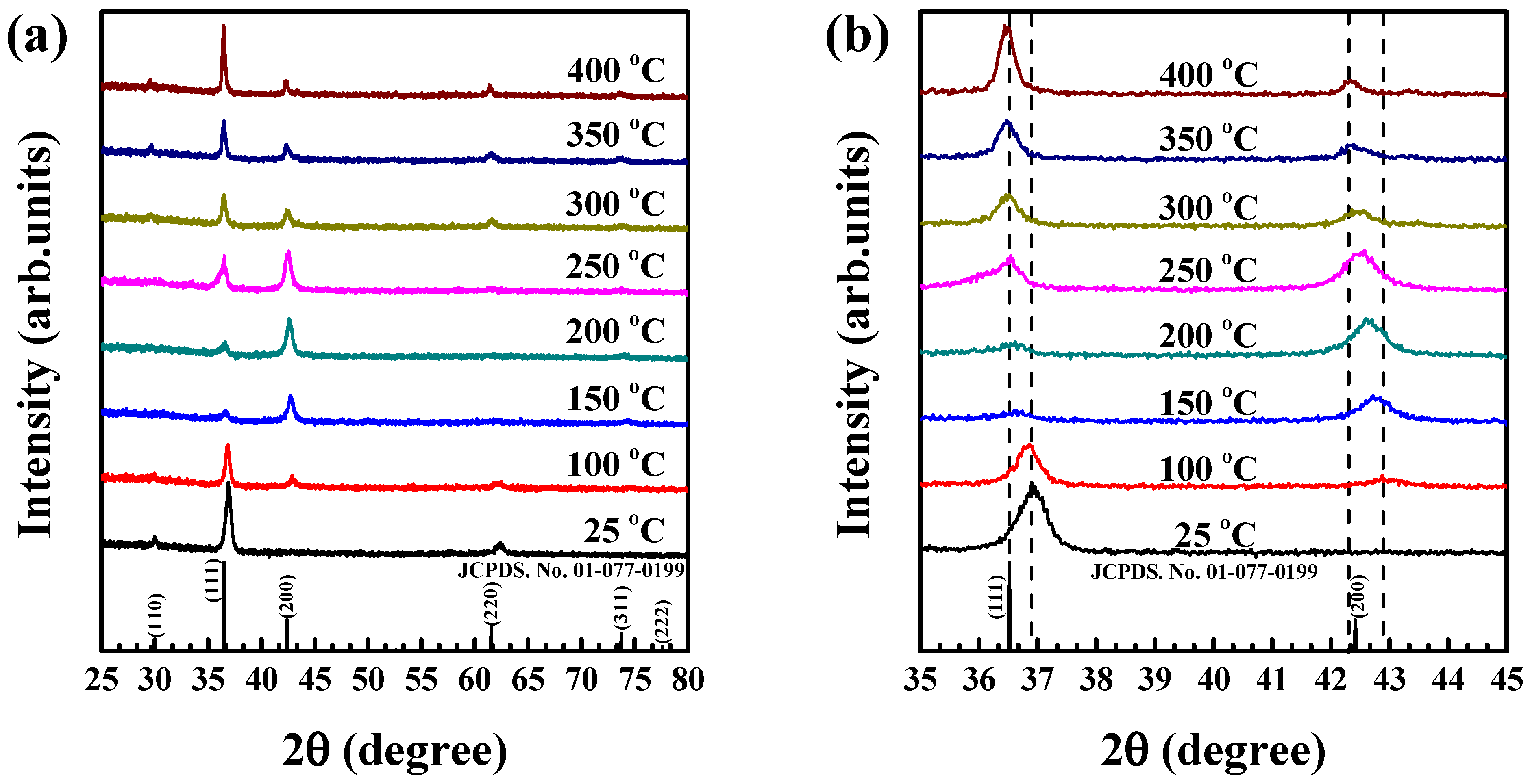
3.1. Structural Analysis of the Cu2O Thin Films

Figure 1a shows the XRD diffraction patterns of the Cu2O films grown at different substrate temperatures with the diffraction angle (2θ) ranging from 25° to 80°. The preferred growth peaks of the Cu2O films grown at substrate temperatures from 25 °C to 200 °C were found around the 2θ diffraction angle of 36.9° or 36.6° for the (111) plane. The main diffraction peaks of the Cu2O films deposited at temperatures from 250 °C to 400 °C were consistent with the 2θ diffraction angle of 36.5°. In addition, four diffraction peaks representing the (110), (200), (220), and (311) planes were detected at 29.6°, 42.3°, 61.4°, and 73.6°, respectively [36]. The diffraction pattern showed that all of the Cu2O films were grown to have a cubic crystalline structure (JCPDS card No.,01-077-0199). Diffraction peaks, such as those of Cu, CuO, and Cu3O4, that corresponded to impurity phases in the Cu2O films were not observed in the XRD pattern. When the substrate temperature was increased from 25 °C to 200 °C, the diffraction intensity for the (111) plane drastically decreased, while that for the (200) plane gradually increased. At a higher substrate temperature of 250 °C, the peak intensity for the (200) plane decreased to a level similar to that for the (111) plane, which was relatively weak. At the substrate temperature of 300 °C or higher, the intensity for the (111) plane again increased, which was opposite to the diffraction results for the Cu2O films deposited at lower temperatures in the range of 150 °C to 250 °C. Figure 1b shows the shifts in the diffraction peaks for the (111) and (200) planes with the increase in the substrate temperature. The peak position for the (111) plane of the Cu2O film deposited at 400 °C was shifted to the left by a diffraction angle of 0.38° in comparison with the as-grown Cu2O film. The diffraction peak for the (200) plane was found for all of the samples deposited at all of the substrate temperatures (100 °C to 400 °C), except for 25 °C. The shift in the diffraction peak to the left was also found in the diffraction peak of the (200) plane, as in the (111) plane. Since identical deposition parameters (operating pressure, flow rate of the reaction gas, RF power, distance from the target to the substrate, etc.)—except for the substrate temperature—were applied for all the deposition samples, the displacement of these diffraction peaks is believed to have been caused by lattice strain effects that depended on the temperature conditions [38]. The lattice strain (ε) values according to the substrate temperature are shown in Table 1.
The crystallite size of the Cu2O films was calculated by substituting the XRD data for the diffraction peaks for the (111) plane into the Debye–Scherrer equation:
D = 0.9 λ β c o s θ
where D is the crystallite size, 0.9 is the Scherrer constant, λ is the X-ray wavelength (0.15418 nm), β is the full width at half maximum (FWHM) of the peaks for the (111) plane, and θ is the Bragg diffraction angle [39]. The details of the crystallite size depending on the Cu2O film deposition parameters are shown in Table 1. The crystallite size of the Cu2O films deposited at substrate temperatures from 25 °C to 200 °C for the (111) plane decreased from 36.4 nm to 18.2 nm as the temperature increased. This may have been due to the reduction in the intensity of the diffraction peak for the (111) plane and the preferred orientation in the (200) direction. At temperatures above 250 °C, the predominant crystal growth orientation changed to the (111) plane; thus, the crystallite size also increased when the temperature was increased. This indicated that the preferential orientation and structural properties of the Cu2O films on the (110) plane were improved by increasing the substrate temperature.

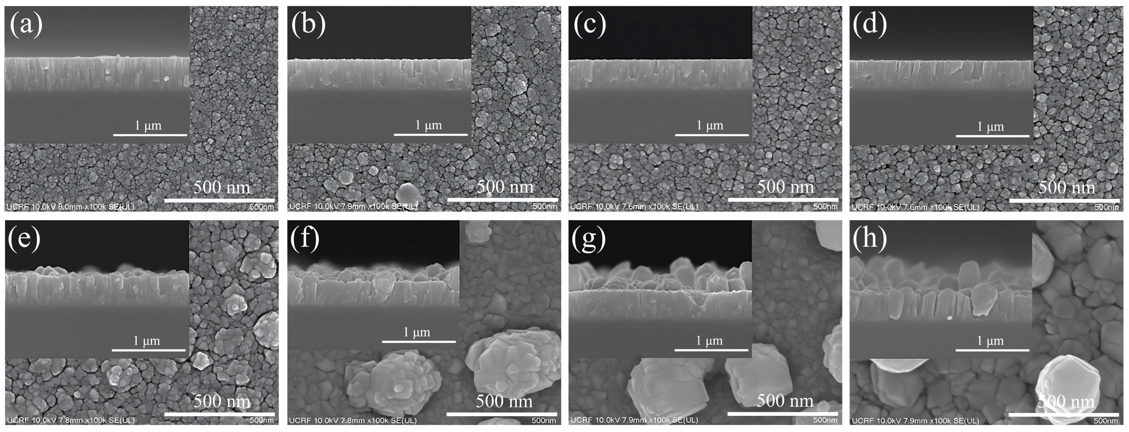
3.2. Morphological Analysis of the Cu2O Thin Films

Figure 2 shows FE-SEM images of the surface and cross-section of Cu2O films that were sputtered for 60 min at various substrate temperatures. The image in Figure 2a shows a uniform distribution of densely packed grains with an average grain size of 26 nm across the surface of the Cu2O thin film deposited at a substrate temperature of 25 °C. As the substrate temperature was increased, the grain size was greatly increased from 45 nm (100 °C) to 129 nm (400 °C), and aggregation of the grains was observed more clearly. This trend of increasing crystal grain size was a result that was different from the crystallite size fluctuation calculated from the XRD measurement data. In particular, over the substrate temperature range of 25 °C to 200 °C, the crystallite size of the samples decreased from 36.4 nm to 18.2 nm with increasing FWHM values. On the other hand, the grain size analyzed in the FE-SEM images in this temperature range improved from 45 nm to 54 nm. The phenomenon in which the grain size in the FE-SEM images was larger than the crystallite size obtained from the XRD data can be found in other studies [40,41]. As depicted in Figure 2, the Cu2O thin films exhibited significant variations in the micro-surface morphology and grain size with increasing substrate temperature. Specifically, as the temperature increased, the grains grew larger, and the surface texture became less uniform. Moreover, the mismatch of expansion coefficients between the film and the substrate led to enlarged voids at the grain boundaries [42].
The average thickness of the Cu2O thin films grown at 25 °C was 436 nm. The thickness of the samples deposited while increasing the substrate temperature revealed a decreasing trend, which resulted in 425 nm at 100 °C, 409 nm at 150 °C, and 405 nm at 200 °C according to each temperature condition. Contrary to this trend, the average thickness of the Cu2O thin films deposited in the higher temperature range from 250 °C to 400 °C was elevated from 436 nm to 444 nm. The decrease in the film thickness in the substrate temperature range from 100 °C to 200 °C was related to the lattice strain, which is recorded in Table 1. The lattice strain (ε) of the sample deposited at 25 °C was 3.14 × 10⁻³. Meanwhile, the lattice strain of the samples deposited at 100 °C, 150 °C, and 200 °C were increased to 4.40 × 10⁻³, 5.05 × 10⁻³, and 6.33 × 10⁻³, respectively, compared to the as-grown sample. When a thin film is grown on a substrate, lattice distortion may occur if the lattice structure of the thin film being formed does not perfectly match the lattice structure of the substrate [43]. As the lattice strain increases, defects such as dislocations and vacancies are formed in the crystalline structure of the thin film, limiting its growth [44,45]. Therefore, the reduction in the thickness of the film in this temperature range is considered to be a result of the increase in the lattice strain occurring during the sputtering deposition of the Cu2O thin film, which acts as a limiting factor for the growth of the thin films.

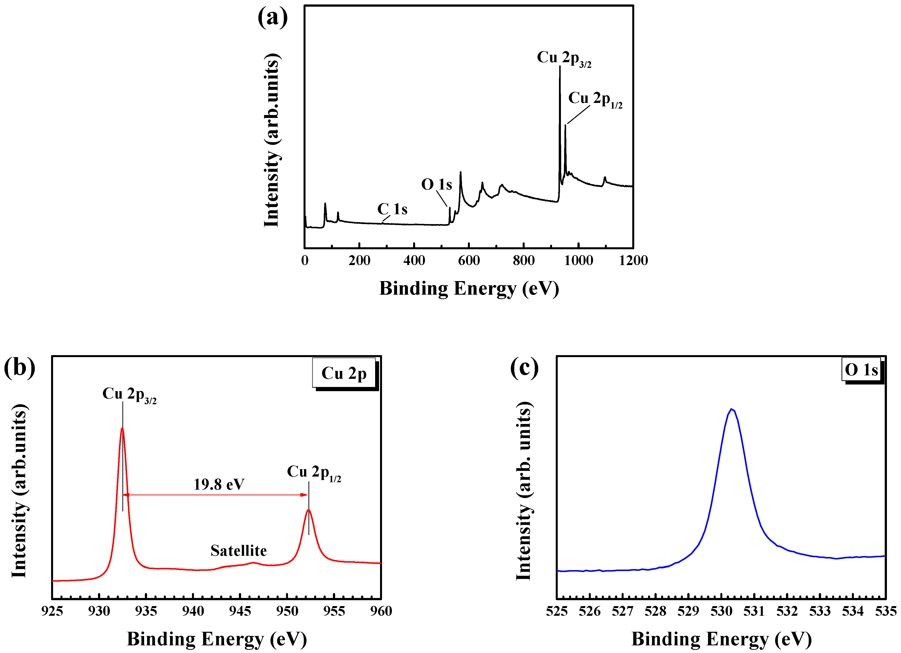
3.3. Chemical Analysis of the Cu2O Thin Films

Figure 3 shows the binding energy (BE) of the Cu2O films and the valence states of the elements analyzed in the XPS data. All of the Cu2O films were etched with argon plasma for 20 s, and energy calibration was performed with reference to the value for C 1s (284.6 eV) [46,47]. Figure 3a shows the XPS spectrum in the BE range of 0 to 1200 eV. The spectrum includes the major spectra representing Cu2O, such as Cu 2p, O 1s, and C 1s. Figure 3b shows the detailed XPS spectrum of Cu 2p. The Cu 2p level had two sub-levels of 2p3/2 and 2p1/2. The BE of Cu 2p3/2 was found to be 932.3 ± 0.2 eV, and that of Cu 2p1/2 was found to be 952.1 ± 0.2 eV, which was consistent with a previous report [48]. As shown in Table 2, the difference in the BE among the Cu2O films depending on the substrate temperature was very slight at 19.8 ± 0.1 eV. In addition, a weak satellite peak for CuO was observed between Cu 2p3/2 and 2p1/2, which meant that a small amount of CuO existed on the surface of the Cu2O films. This result—that a trace amount of CuO was present on the surface of the Cu2O film—contradicted the XRD results analyzed in Figure 1. According to the state diagram of copper and oxygen, of the Cu2O, Cu4O3, and CuO phases, the CuO phase is the most stable under atmospheric conditions [49]. Therefore, when an as-deposited metastable Cu2O film is exposed to the atmosphere, it can be expected that Cu2O will oxidize into CuO on the film surface. Due to this, it is believed that weak satellite peaks in Cu2O were observed in the XPS spectrum. Figure 3c shows the BE spectrum of O 1s. The O 1s level was the BE corresponding to the lattice oxygen (O2−) of Cu2O found in the range of 530 to 530.3 eV. This was precisely consistent with the previously reported value [50]. Therefore, the XPS results confirmed that the prepared samples were made of Cu2O.

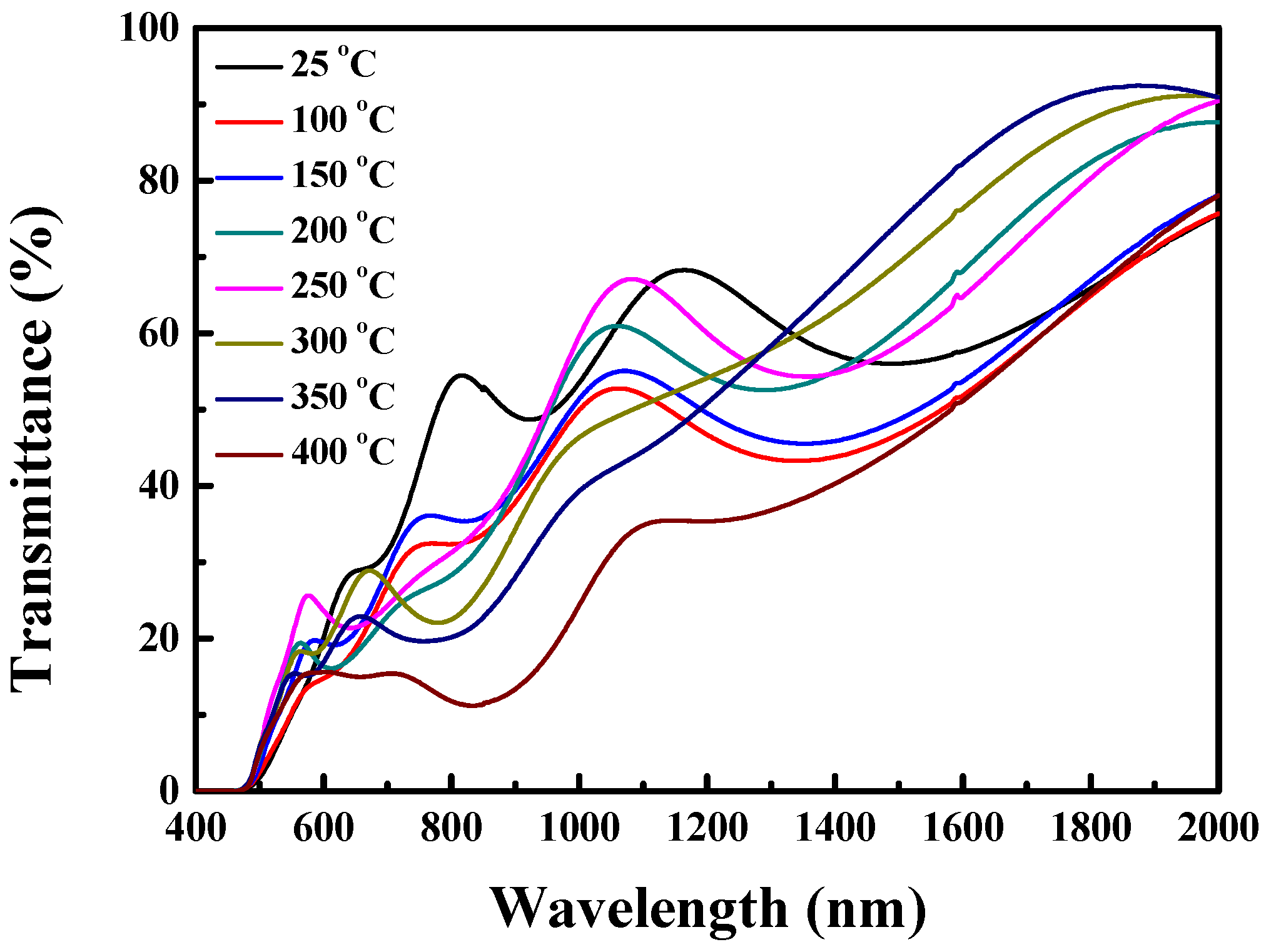
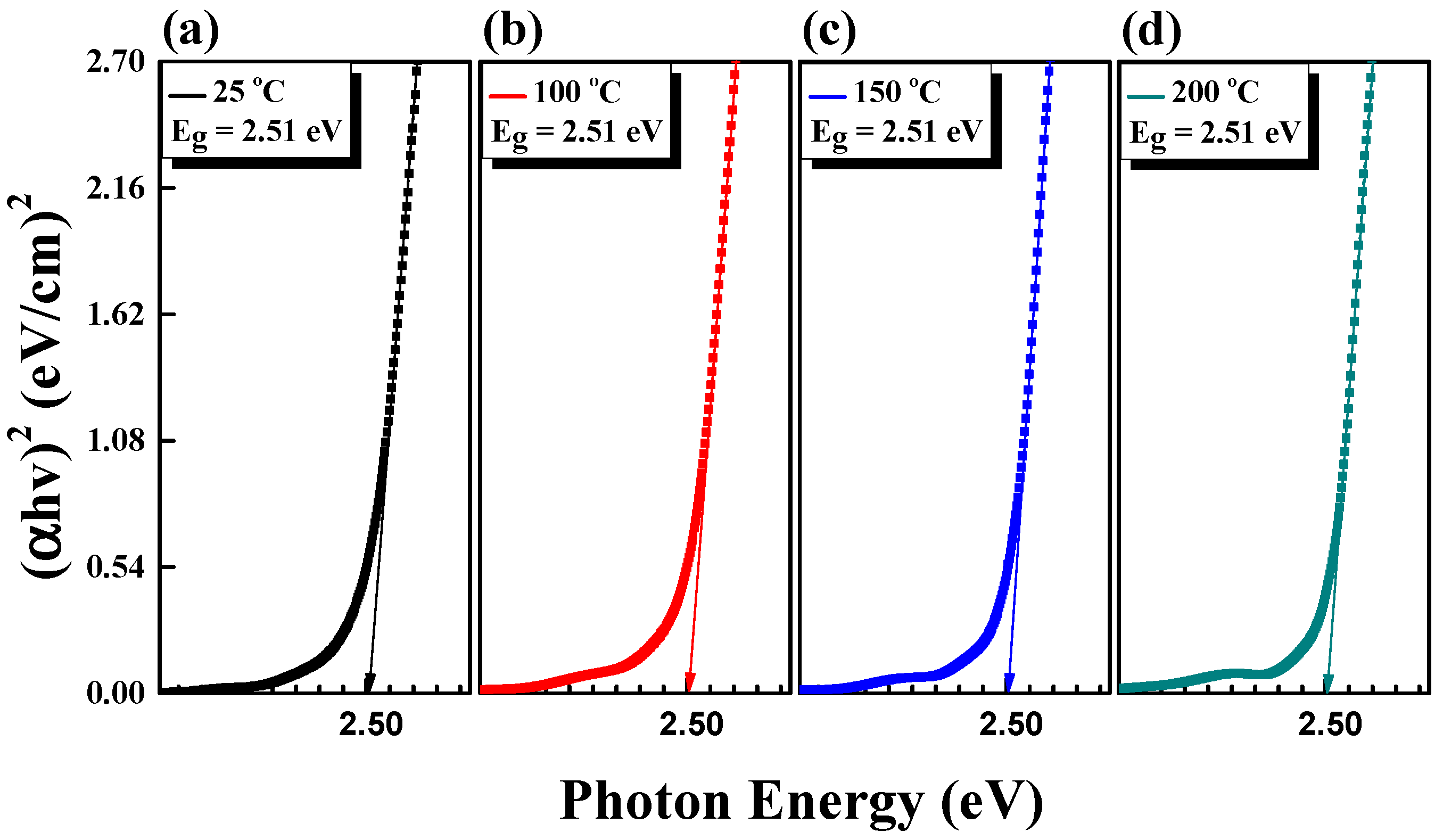
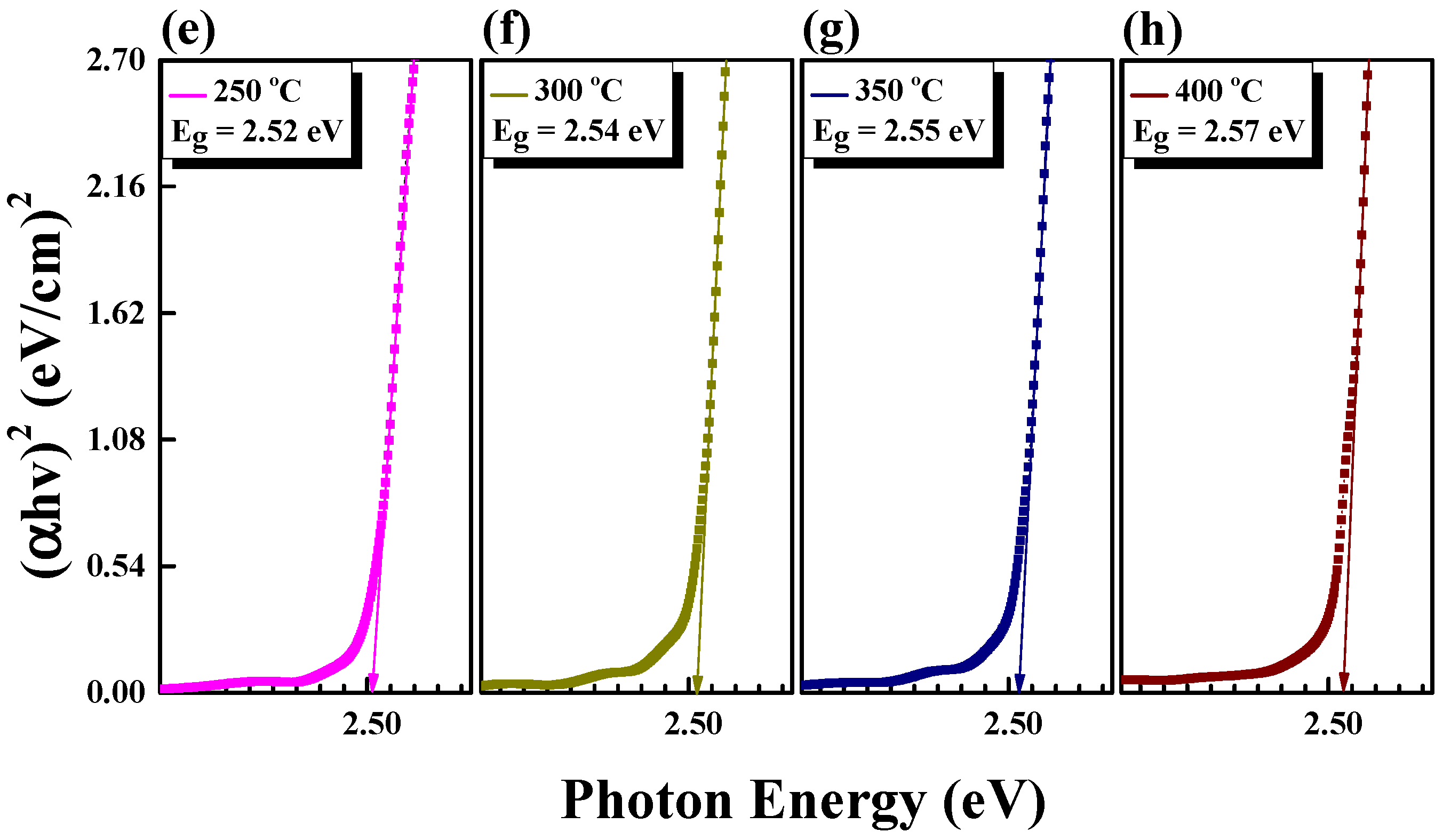
3.4. Optical Analysis of the Cu2O Thin Films

Figure 4 shows the light transmittance spectra of the Cu2O films prepared at substrate temperatures from 25 °C to 400 °C, and the measurements were performed in a wavelength range from 400 to 2000 nm. The transmittance values in specific regions (visible and near-infrared rays) can be found in Table 3, along with the average transmittance values of the Cu2O films. The average transmittance of the Cu2O thin film deposited at a substrate temperature of 25 °C was 50.2%, and as the temperature increased, the transmittance of the film decreased to 34.3% at 400 °C. The reduction in the transmittance was closely related to the size and shape of the grains forming the fine surface of the film. As observed in the FE-SEM surface morphology in Figure 2, the grain size of the Cu2O thin film deposited via sputtering significantly increased as the substrate temperature increased. This increase in grain size created more crystallographic boundaries within the film. More crystallographic boundaries cause further scattering and absorption of light within a Cu2O thin film, thus reducing the average transmittance of the film [37,51,52]. Therefore, as the substrate temperature increases, the optical properties of the film change due to the increased crystallographic boundary, resulting in a decrease in the average transmittance. In the visible region (λ = 400 to 750 nm), the transmittance was decreased from 15.9% (25 °C) to 10.1% (400 °C). In the near-infrared region (λ = 750 to 2000 nm), the transmittance was also reduced from 60.2% (25 °C) to 41.7% (400 °C) as the substrate temperature was increased.
The optical band gap energy (Eg) of the Cu2O films was calculated from the light transmittance data using the Tauc equation:
α = 2.303 d l o g 10 % T
( α h ν ) 1 / n = A ( h ν E g )
where α is the absorption coefficient of the film calculated with Equation (2). In Equation (2), d represents the film thickness and T represents the transmittance. In Equation (3), h is the Planck constant, ν is the photon’s frequency, A is the proportionality constant, and Eg is the optical energy band gap [53]. In addition, the value of n is a coefficient that represents the electronic transition of a semiconductor; the value of n is 0.5 or 2 in the case of a direct band or an indirect band, respectively. Since Cu2O generally has a direct band structure, n = 0.5 was used [54].
Figure 5 shows the band gaps of the Cu2O films based on the Tauc plot. The Eg was constant from 25 °C to 200 °C. When the substrate temperature was increased in steps from 250 °C to 350 °C in 50 °C increments, the value of Eg slightly increased. The highest Eg value of 2.57 eV was measured at a substrate temperature of 400 °C. These results matched well with the previously reported Cu2O band gap energy values (2.1 to 2.6 eV) [55,56]. The energy band gap of the Cu2O thin films deposited via sputtering could increase with increasing substrate temperature due to changes in the microstructure and chemical composition of the thin films. Films grown at relatively low substrate temperatures were typically amorphous or contained small crystallites. Conversely, as the substrate temperature increased, the crystallites became larger, and the crystallinity of the film improved. This can be explained by the Burstein–Moss effect (blue shift), which refers to the expansion of the energy band gap by changing the electronic band structure of a film [57,58].

4. Conclusions

Cu2O films were prepared on glass substrates via RF magnetron sputtering at various substrate temperatures (25 °C to 400 °C). XRD analysis showed that all of the Cu2O films had a cubic structure. As the substrate temperature was increased from 25 °C to 200 °C, the diffraction intensity for the (111) plane gradually decreased, while the peak intensity for the (200) plane increased. On the contrary, at a higher substrate temperature of 250 °C, the peak intensity for the (111) plane increased again and the peak intensity for the (200) plane changed to a level that was slightly higher than the peak intensity for the (111) plane. From 300 °C, the preferred orientation of the (111) plane was maintained. The crystallite size, which was determined via FE-SEM, was increased when the substrate temperature was increased. XPS analysis showed that the binding energy (BE) of the Cu2O film sputtered at 400 °C in the present study was very similar to a previously reported value. The as-grown Cu2O film showed the highest transmittance (15.9%) in the visible region, which decreased as the substrate temperature increased. The energy band gap (Eg) remained the same (2.51 eV) at 25 °C and 200 °C, as it was not affected by the experimental parameter. The Eg was increased when the temperature was increased from 250 °C (2.52 eV) to 400 °C (2.57 eV). In conclusion, substrate temperature plays a critical role in determining the structural, compositional, and optical properties of Cu2O films grown via RF magnetron sputtering. Our results suggest that the preferred orientation of the (111) plane is maintained above 300 °C, and the crystallite size increases with increases in the substrate temperature. The energy band gap also exhibits a slight increase when the substrate temperature is increased to 400 °C. Further studies are necessary to investigate the potential of Cu2O films for various applications, such as solar cells and electro-optical devices.

Author Contributions

Conceptualization, J.-A.K. and D.-H.H.; methodology, C.-S.S. and Y.-G.S.; validation, S.-G.P. and D.-H.H.; formal analysis, J.-A.K. and J.-H.P.; investigation, J.-A.K. and J.-H.P.; resources, C.-S.S. and Y.-G.S.; data curation, S.-G.P.; writing—original draft preparation, J.-A.K.; writing—review and editing, Y.-G.S. and D.-H.H.; visualization, J.-A.K. and J.-H.P.; supervision, S.-G.P., C.-S.S. and Y.-G.S.; project administration, D.-H.H.; funding acquisition, C.-S.S. and D.-H.H. All authors have read and agreed to the published version of the manuscript.

Funding

This work was supported by the National Research Foundation of Korea (NRF) grant funded by the Korean government (MSIT) (No. NRF-2018R1A5A1025594), and it was supported by the Korea Institute of Energy Technology Evaluation and Planning (KETEP) grant funded by the Korean government (MOTIE) (20213030010140, The study on 200 kW demonstration and development of fence-type photovoltaics in rural area satisfying LCOE 140.8 (/kWh)).

Data Availability Statement

The data presented or analyzed in this study are available from the corresponding author upon reasonable request.

Conflicts of Interest

The authors declare no conflict of interest.

References

  1. Umar, M.; Swinkels, M.Y.; De Luca, M.; Fasolato, C.; Moser, L.; Gadea, G.; Marot, L.; Glatzel, T.; Zardo, I. Morphological and stoichiometric optimization of Cu2O thin films by deposition conditions and post-growth annealing. Thin Solid Film. 2021, 732, 138763. [Google Scholar] [CrossRef]
  2. Jose, R.; Thavasi, V.; Ramakrishna, S. Metal Oxides for Dye-Sensitized Solar Cells. J. Am. Ceram. Soc. 2009, 92, 289–301. [Google Scholar] [CrossRef]
  3. Petti, L.; Münzenrieder, N.; Vogt, C.; Faber, H.; Büthe, L.; Cantarella, G.; Bottacchi, F.; Anthopoulos, T.D.; Tröster, G. Metal oxide semiconductor thin-film transistors for flexible electronics. Appl. Phys. Rev. 2016, 3, 021303. [Google Scholar] [CrossRef] [Green Version]
  4. Siol, S.; Hellmann, J.C.; Tilley, S.D.; Graetzel, M.; Morasch, J.; Deuermeier, J.; Jaegermann, W.; Klein, A. Band Alignment Engineering at Cu2O/ZnO Heterointerfaces. ACS Appl. Mater. Interfaces 2016, 8, 21824–21831. [Google Scholar] [CrossRef] [PubMed]
  5. Jahangir-Moghadam, M.; Ahmadi-Majlan, K.; Shen, X.; Droubay, T.; Bowden, M.; Chrysler, M.; Su, D.; Chambers, S.A.; Ngai, J.H. Band-Gap Engineering at a Semiconductor-Crystalline Oxide Interface. Adv. Mater. Interfaces 2015, 2, 1400497. [Google Scholar] [CrossRef] [Green Version]
  6. Boyd, C.C.; Shallcross, R.C.; Moot, T.; Kerner, R.; Bertoluzzi, L.; Onno, A.; Kavadiya, S.; Chosy, C.; Wolf, E.J.; Werner, J.; et al. Overcoming Redox Reactions at Perovskite-Nickel Oxide Interfaces to Boost Voltages in Perovskite Solar Cells. Joule 2020, 4, 1759–1775. [Google Scholar] [CrossRef]
  7. Pandian, M.G.M.; Khadka, D.B.; Shirai, Y.; Yanagida, M.; Kitamine, S.; Alghamdi, A.R.M.; Subashchandran, S.; Miyano, K. Effect of surface treatment of sputtered nickel oxide in inverted perovskite solar cells. Thin Solid Film. 2022, 760, 139486. [Google Scholar] [CrossRef]
  8. Tseng, Z.-L.; Chen, L.-C.; Chiang, C.-H.; Chang, S.-H.; Chen, C.-C.; Wu, C.-G. Efficient inverted-type perovskite solar cells using UV-ozone treated MoOx and WOx as hole transporting layers. Sol. Energy 2016, 139, 484–488. [Google Scholar] [CrossRef]
  9. Reyes-Vallejo, O.; Sanchez-Albores, R.M.; Fernandez-Madrigal, A.; Cano, F.J.; Meza-Avendano, C.A.; Diaz, J.J.; Ashok, A.; Sebastian, P.J. Chemical Bath Deposition of Cu2O Thin Films on FTO Substrates: Effect of Sequential Deposition. In Proceedings of the 2022 19th International Conference on Electrical Engineering, Computing Science and Automatic Control (CCE), Mexico City, Mexico, 9–11 November 2022; pp. 1–6. [Google Scholar] [CrossRef]
  10. Farhad, S.F.U.; Hossain, M.A.; Tanvir, N.I.; Akter, R.; Patwary, M.A.M.; Shahjahan, M.; Rahman, M.A. Structural, optical, electrical, and photoelectrochemical properties of cuprous oxide thin films grown by modified SILAR method. Mater. Sci. Semicond. Process. 2019, 95, 68–75. [Google Scholar] [CrossRef]
  11. Zhang, M.; He, X.; Xue, Y.; Lin, Z.; Tong, N.-H.; Lai, W.; Liang, S. Improving thermoelectric properties of Cu2O powder via interface modification. Solid State Commun. 2022, 357, 114982. [Google Scholar] [CrossRef]
  12. Xu, M.; Liu, X.; Xu, W.; Xu, H.; Hao, X.; Feng, X. Low resistivity phase-pure n-type Cu2O films realized via post-deposition nitrogen plasma treatment. J. Alloys Compd. 2018, 769, 484–489. [Google Scholar] [CrossRef]
  13. Özdal, T.; Kavak, H. Fabrication and characterization of ZnO/Cu2O heterostructures for solar cells applications. Superlattices Microstruct. 2020, 146, 106679. [Google Scholar] [CrossRef]
  14. Al-Jawhari, H.A. A review of recent advances in transparent p-type Cu2O-based thin film transistors. Mater. Sci. Semicond. Process. 2015, 40, 241–252. [Google Scholar] [CrossRef]
  15. Kajli, S.K.; Ray, D.; Roy, S.C. Efficient UV–visible photodetector based on single CuO/Cu2O core-shell nanowire. J. Alloys Compd. 2022, 895, 162546. [Google Scholar] [CrossRef]
  16. Pu, F.; Miao, H.; Lu, W.; Zhang, X.; Yang, Z.; Kong, C. High-performance non-enzymatic glucose sensor based on flower-like Cu2O-Cu-Au ternary nanocomposites. Appl. Surf. Sci. 2022, 581, 152389. [Google Scholar] [CrossRef]
  17. Wang, M.; Zhang, X.; He, X.; Zhu, B.; Tang, H.; Wang, C. In-situ grown flower-like C@SnO2/Cu2O nanosheet clusters on Cu foam as high performance anode for lithium-ion batteries. J. Alloys Compd. 2021, 856, 158202. [Google Scholar] [CrossRef]
  18. Wu, N.; Wu, H.; Zhang, J.; Zhang, Y.; Cao, D.; Bai, L.; Hu, T. Cu2O/Cu@C nanosheets derived from one novel Cu (II) metal-organic framework for high performance supercapacitors. J. Alloys Compd. 2021, 856, 157466. [Google Scholar] [CrossRef]
  19. Wang, Y.; Miska, P.; Pilloud, D.; Horwat, D.; Mücklich, F.; Pierson, J.F. Transmittance enhancement and optical band gap widening of Cu2O thin films after air annealing. J. Appl. Phys. 2014, 115, 073505. [Google Scholar] [CrossRef]
  20. Minami, T.; Nishi, Y.; Miyata, T. Efficiency enhancement using a Zn1−xGex-O thin film as an n-type window layer in Cu2O-based heterojunction solar cells. Appl. Phys. Express 2016, 9, 052301. [Google Scholar] [CrossRef]
  21. Alajlani, Y.; Placido, F.; Chu, H.O.; De Bold, R.; Fleming, L.; Gibson, D. Characterisation of Cu2O/CuO thin films produced by plasma-assisted DC sputtering for solar cell application. Thin Solid Film. 2017, 642, 45–50. [Google Scholar] [CrossRef] [Green Version]
  22. El Kasmi, A.; Tian, Z.-Y.; Vieker, H.; Beyer, A.; Chafik, T. Innovative CVD synthesis of Cu2O catalysts for CO oxidation. Appl. Catal. B Environ. 2016, 186, 10–18. [Google Scholar] [CrossRef]
  23. Farhad, S.F.U.; Cherns, D.; Smith, J.A.; Fox, N.A.; Fermín, D.J. Pulsed laser deposition of single phase n- and p-type Cu2O thin films with low resistivity. Mater. Des. 2020, 193, 108848. [Google Scholar] [CrossRef]
  24. Liau, L.C.-K.; Lin, Y.-C.; Peng, Y.-J. Fabrication Pathways of p–n Cu2O Homojunction Films by Electrochemical Deposition Processing. J. Phys. Chem. C 2013, 117, 26426–26431. [Google Scholar] [CrossRef]
  25. Gudmundsson, J.T. Physics and technology of magnetron sputtering discharges. Plasma Sources Sci. Technol. 2020, 29, 113001. [Google Scholar] [CrossRef]
  26. Oka, N.; Watanabe, M.; Sugie, K.; Iwabuchi, Y.; Kotsubo, H.; Shigesato, Y. Reactive-gas-flow sputter deposition of amorphous WO3 films for electrochromic devices. Thin Solid Film. 2013, 532, 1–6. [Google Scholar] [CrossRef]
  27. Nair, A.S.; Abraham, J.E.; George, P.; Joseph, C.; Biju, P.; Unnikrishnan, N.; Saritha, A. Effect of substrate temperature on the near-infrared shielding properties of WO3-X thin films deposited by RF magnetron sputtering. Vacuum 2022, 202, 111143. [Google Scholar] [CrossRef]
  28. Pérez-González, M.; Morales-Luna, M.; Santoyo-Salazar, J.; Crotte-Ledesma, H.; García-Tinoco, P.E.; Tomás, S.A. Improved adsorption and photocatalytic removal of methylene blue by MoO3 thin films: Role of the sputtering power, film thickness, and sputtering working pressure. Catal. Today 2021, 360, 138–146. [Google Scholar] [CrossRef]
  29. Yu, S.; Xu, W.; Zhu, H.; Qiu, W.; Fu, Q.; Kong, L. Effect of sputtering power on structure and properties of ZTO films. J. Alloys Compd. 2021, 883, 160622. [Google Scholar] [CrossRef]
  30. Yang, F.; Peng, W.; Zhou, Y.; Li, R.; Xiang, G.; YueLiu, J.Z.; Zhang, J.; Zhao, Y.; Wang, H. Thermal optimization of defected Cu2O photon-absorbing layer and the steady p-Cu2O/n-Si photovoltaic application. Vacuum 2022, 198, 110876. [Google Scholar] [CrossRef]
  31. Dolai, S.; Das, S.; Hussain, S.; Bhar, R.; Pal, A.K. Cuprous oxide (Cu2O) thin films prepared by reactive d.c. sputtering technique. Vacuum 2017, 141, 296–306. [Google Scholar] [CrossRef]
  32. Sivasankar Reddy, A.; Sreedhara Reddy, P.; Uthanna, S.; Venkata Rao, G.; Klein, A. Effect of substrate temperature on the physical properties of dc magnetron sputtered Cu2O films. Phys. Status Solidi 2006, 203, 844–853. [Google Scholar] [CrossRef]
  33. Lee, S.H. The Characteristics of Cu2O Thin Films Deposited Using RF-Magnetron Sputtering Method with Nitrogen-Ambient. ETRI J. 2013, 35, 1156–1159. [Google Scholar] [CrossRef]
  34. Ishizuka, S.; Maruyama, T.; Akimoto, K. Thin-film deposition of Cu2O by reactive radio-frequency magnetron sputtering. Jpn. J. Appl. Phys. 2000, 39, L786. [Google Scholar] [CrossRef]
  35. Han, S.; Flewitt, A.J. Control of grain orientation and its impact on carrier mobility in reactively sputtered Cu2O thin films. Thin Solid Film. 2020, 704, 138000. [Google Scholar] [CrossRef]
  36. Peng, W.; Zhou, Y.; Li, J.; Liu, Y.; Zhang, J.; Xiang, G.; Zhu, X.; Li, R.; Wang, H.; Zhao, Y. Annealing temperature induced physical characteristics of CuO films grown by magnetron sputtering. Mater. Sci. Semicond. Process. 2021, 131, 105883. [Google Scholar] [CrossRef]
  37. Kim, H.-S.; Yadav, P.; Patel, M.; Kim, J.; Pandey, K.; Lim, D.; Jeong, C. Transparent Cu4O3/ZnO heterojunction photoelectric devices. Superlattices Microstruct. 2017, 112, 262–268. [Google Scholar] [CrossRef]
  38. Grez, P.; Herrera, F.; Riveros, G.; Ramírez, A.; Henríquez, R.; Dalchiele, E.; Schrebler, R. Morphological, structural, and photoelectrochemical characterization of n-type Cu2O thin films obtained by electrodeposition. Phys. Status Solidi 2012, 209, 2470–2475. [Google Scholar] [CrossRef]
  39. Gan, J.; Venkatachalapathy, V.; Svensson, B.G.; Monakhov, E.V. Influence of target power on properties of CuxO thin films prepared by reactive radio frequency magnetron sputtering. Thin Solid Film. 2015, 594, 250–255. [Google Scholar] [CrossRef]
  40. Messier, R. Toward quantification of thin film morphology. J. Vac. Sci. Technol. A Vac. Surf. Film. 1986, 4, 490–495. [Google Scholar] [CrossRef]
  41. Basak, M.; Rahman, L.; Ahmed, F.; Biswas, B.; Sharmin, N. The use of X-ray diffraction peak profile analysis to determine the structural parameters of cobalt ferrite nanoparticles using Debye- Scherrer, Williamson-Hall, Halder-Wagner and Size-strain plot: Different precipitating agent approach. J. Alloys Compd. 2022, 895, 162694. [Google Scholar] [CrossRef]
  42. Basak, M.; Rahman, L.; Ahmed, F.; Biswas, B.; Sharmin, N. Calcination effect on structural, morphological and magnetic properties of nano-sized CoFe2O4 developed by a simple co-precipitation technique. Mater. Chem. Phys. 2021, 264, 124442. [Google Scholar] [CrossRef]
  43. Han, H.; Park, J.; Nam, S.Y.; Kim, K.J.; Choi, G.M.; Parkin, S.S.P.; Jang, H.M.; Irvine, J.T.S. Lattice strain-enhanced exsolution of nanoparticles in thin films. Nat. Commun. 2019, 10, 1471. [Google Scholar] [CrossRef] [PubMed] [Green Version]
  44. Kaya, S.; Yilmaz, E.; Karacali, H.; Cetinkaya, A.O.; Aktag, A. Samarium oxide thin films deposited by reactive sputtering: Effects of sputtering power and substrate temperature on microstructure, morphology and electrical properties. Mater. Sci. Semicond. Process. 2015, 33, 42–48. [Google Scholar] [CrossRef]
  45. Han, H.; Kim, D.; Chu, K.; Park, J.; Nam, S.Y.; Heo, S.; Yang, C.H.; Jang, H.M. Enhanced Switchable Ferroelectric Photovoltaic Effects in Hexagonal Ferrite Thin Films via Strain Engineering. ACS Appl. Mater. Interfaces 2018, 10, 1846–1853. [Google Scholar] [CrossRef]
  46. Devaraj, M.; Saravanan, R.; Deivasigamani, R.; Gupta, V.K.; Gracia, F.; Jayadevan, S. Fabrication of novel shape Cu and Cu/Cu2O nanoparticles modified electrode for the determination of dopamine and paracetamol. J. Mol. Liq. 2016, 221, 930–941. [Google Scholar] [CrossRef]
  47. Greczynski, G.; Hultman, L. Compromising Science by Ignorant Instrument Calibration-Need to Revisit Half a Century of Published XPS Data. Angew. Chem. Int. Ed. Engl. 2020, 59, 5002–5006. [Google Scholar] [CrossRef]
  48. Al-Kuhaili, M.F. Characterization of copper oxide thin films deposited by the thermal evaporation of cuprous oxide (Cu2O). Vacuum 2008, 82, 623–629. [Google Scholar] [CrossRef]
  49. Xu, C.H.; Woo, C.H.; Shi, S.Q. Formation of CuO nanowires on Cu foil. Chem. Phys. Lett. 2004, 399, 62–66. [Google Scholar] [CrossRef]
  50. Hossain, M.A.; Al-Gaashani, R.; Hamoudi, H.; Al Marri, M.J.; Hussein, I.A.; Belaidi, A.; Merzougui, B.A.; Alharbi, F.H.; Tabet, N. Controlled growth of Cu2O thin films by electrodeposition approach. Mater. Sci. Semicond. Process. 2017, 63, 203–211. [Google Scholar] [CrossRef]
  51. Ibrahim, A.M.; Abdel-wahab, M.S.; Elfayoumi, M.A.K.; Tawfik, W.Z. Highly efficient sputtered Ni-doped Cu2O photoelectrodes for solar hydrogen generation from water-splitting. Int. J. Hydrog. Energy 2023, 48, 1863–1876. [Google Scholar] [CrossRef]
  52. Marzuki, M.; Mohamad Zain, M.Z.; Hisham, N.Z.; Zainon, N.; Harun, A.; Ahmad, R.N. Annealing Effects on the Formation of Copper Oxide Thin Films. IOP Conf. Ser. Mater. Sci. Eng. 2018, 318, 012060. [Google Scholar] [CrossRef]
  53. Nyborg, M.; Azarov, A.; Bergum, K.; Monakhov, E. Deposition and characterization of lithium doped direct current magnetron sputtered Cu2O films. Thin Solid Film. 2021, 722, 138573. [Google Scholar] [CrossRef]
  54. Saikumar, A.K.; Sundaresh, S.; Nehate, S.D.; Sundaram, K.B. Properties of RF Magnetron-Sputtered Copper Gallium Oxide (CuGa2O4) Thin Films. Coatings 2021, 11, 921. [Google Scholar] [CrossRef]
  55. Sai Guru Srinivasan, S.; Govardhanan, B.; Aabel, P.; Ashok, M.; Santhosh Kumar, M.C. Effect of oxygen partial pressure on the tuning of copper oxide thin films by reactive sputtering for solar light driven photocatalysis. Sol. Energy 2019, 187, 368–378. [Google Scholar] [CrossRef]
  56. Sai Guru Srinivasan, S.; Govardhanan, B.; Ashok, M.; Santhosh Kumar, M.C. Influence of deposition time on the visible-light-driven photocatalytic activity of Cu2O thin films by reactive sputtering at room temperature. Mater. Lett. 2021, 284, 128980. [Google Scholar] [CrossRef]
  57. Koshy, A.M.; Sudha, A.; Yadav, S.K.; Swaminathan, P. Effect of substrate temperature on the optical properties of DC magnetron sputtered copper oxide thin films. Phys. B Condens. Matter 2023, 650, 414452. [Google Scholar] [CrossRef]
  58. Burstein, E. Anomalous Optical Absorption Limit in InSb. Phys. Rev. 1954, 93, 632–633. [Google Scholar] [CrossRef]
Figure 1. XRD analysis results of Cu2O thin films grown at various substrate temperatures; (a) diffraction patterns measured with 2θ angle ranging from 25° to 80°; and (b) detailed movement status of diffraction peaks for the (111) and (200) planes.
Crystals 13 00643 g001
Figure 2. FE-SEM images of the surface and thickness of Cu2O thin films grown at various substrate temperatures: (a) 25 °C, (b) 100 °C, (c) 150 °C, (d) 200 °C, (e) 250 °C, (f) 300 °C, (g) 350 °C, and (h) 400 °C.
Crystals 13 00643 g002
Figure 3. XPS spectra of a Cu2O thin film grown at a substrate temperature of 400 °C; (a) all surveyed spectra, (b) Cu 2p, and (c) O 1s peaks.
Crystals 13 00643 g003
Figure 4. Transmittance spectra of Cu2O thin films deposited in the substrate temperature range from 25 °C to 400 °C.
Crystals 13 00643 g004
Figure 5. Optical energy band gaps of Cu2O thin films deposited in the substrate temperature range from 25 °C to 400 °C: (a) 25 °C, (b) 100 °C, (c) 150 °C, (d) 200 °C, (e) 250 °C, (f) 300 °C, (g) 350 °C, and (h) 400 °C.
Crystals 13 00643 g005aCrystals 13 00643 g005b
Table 1. The crystallite size (determined via XRD), lattice strain (determined via XRD), grain size (determined from FE-SEM images), and thickness (determined from FE-SEM images) of Cu2O thin films grown at various substrate temperatures.
Substrate
Temperature
(°C)
Bragg Angle
2θ
(deg)
FWHM
β
(rad)
Crystallite
Size D
(nm)
Lattice
Strain ε
(10−3)
Grain
Size
(nm)
Film
Thickness
(nm)
2536.8980.24036.43.1426461
10036.8470.33626.04.4045425
15036.6780.38422.85.0550409
20036.6090.48018.26.3354405
25036.5520.24036.43.1759436
30036.5480.33626.04.4471396
35036.4590.19245.52.5491420
40036.5220.26433.13.49129444
Table 2. XPS analysis results for Cu2O thin films deposited at various substrate temperatures.
Substrate Temperature
(°C)
Binding Energy (eV)BE Differences
in Cu 2p
(eV)
Cu 2p/32Cu 2p1/2O 1s
25932.3952.1530.119.8
100932.3952.1530.119.8
150932.3952.0530.019.7
200932.1951.9530.019.8
250932.2952.1530.119.9
300932.3952.1530.219.8
350932.3952.2530.219.9
400932.5952.3530.319.8
Table 3. Average transmittance and optical energy band gap values of Cu2O thin films deposited at various substrate temperatures.
Substrate
Temperature
(°C)
Transmittance
400–2000 nm
(%)
Visible Region
400–750 nm
(%)
Near-infrared Region
750–2000 nm
(%)
Optical Energy
Band Gap
(eV)
2550.215.960.22.51
10041.912.750.52.51
15044.114.952.72.51
20049.913.160.82.51
25051.115.661.22.52
30051.415.262.12.54
35050.912.962.12.55
40034.310.141.72.57
Disclaimer/Publisher’s Note: The statements, opinions and data contained in all publications are solely those of the individual author(s) and contributor(s) and not of MDPI and/or the editor(s). MDPI and/or the editor(s) disclaim responsibility for any injury to people or property resulting from any ideas, methods, instructions or products referred to in the content.

