1. Introduction
With the continuous development of the green information society, the problem of environmental pollution caused by lead volatilization from commercial mainstream ferroelectric devices is becoming increasingly serious. There is a great demand for research on novel high–performance lead–free perovskite materials in the modern society [
1,
2,
3]. (Bi
0.5Na
0.5)TiO
3 (BNT), one of the typical lead-free ferroelectric materials, has received close attention due to its outstanding strain responses in applications involving high-precision actuators [
4]. S.–T. Zhang et al. first reported high–strain (K
0.5Na
0.5)NbO
3 modified BNT–BaTiO
3 (BNT–BT–KNN) with a large strain performance of 0.45% in 2007 [
5]. Subsequently, X.L. Tan et al. achieved an enhanced electro–strain value of 0.70% in BNT ceramics with the substitution of Nb element (BNT–2.5Nb) on the B–site [
6]. In addition, for ferroelectric thin films, important components in semiconductor technologies, it is urgent to improve electrical performance and decrease the leakage [
7]. Many key issues must be seriously considered, such as large leakage and loss, complex composition control, and electrical properties enhancement [
3]. Therefore, realizing BNT–based thin films with good electrical properties and decreased leakage faces many challenges.
Among many deposition technologies for thin films, chemical solution deposition (CSD) is cost–effective and suitable for preparing films with complex compositions [
8,
9,
10,
11]. The heating process for the conversion of solution–deposited uncrystallized layers into shaped thin films plays a significant effect on the crystallization and electrical performances of the films [
12]. For BNT–based materials in the form of thin films, the volatility of alkali metal elements such as Na and Bi during heating limits the annealing treatment to a lower temperature range. Compared with their ceramic counterparts, the characteristics of BNT–based films, e.g., grain size and holes on the surface and inside the films, have important impacts on the dielectric/ferroelectric properties. Therefore, realizing high–quality BNT–based films need a serious control of the experimental procedure and an effective annealing treatment. Post–annealing treatment is a common method for as–deposited thin films. After post–annealing at 700 °C for 20 min, the quality and performance of PbZr
0.3Ti
0.7O
3 (PZT) films were significantly improved: the surface was smoother, and both ferroelectric and pyroelectric properties were improved [
13]. (K
0.5Na
0.5)NbO
3 (KNN) thin films exhibited enhanced electrical properties and ameliorated leakage after post–annealing [
14]. In addition, annealing treatments in certain atmospheres, such as O
2 and N
2, applied to the ferroelectric materials in ceramics and thin films have also been researched [
15,
16]. Annealing the film at a high temperature in an O
2 atmosphere forces oxygen vacancies to appear on the film surface, filling them with oxygen, and promoting the growth of the grains [
17]. The films gradually become denser, with increased grain size and grain uniformity. Improved energy storage properties of Ba
0.85Ca
0.15Ti
0.90Zr
0.10O
3 (BCZT) thin films were obtained by annealing in an oxygen–enriched atmosphere [
18]. That is to say, annealing in an O
2 atmosphere is a useful method to optimize the quality and electrical properties of BNT–based thin films.
2. Experiments
In this work, 0.945(Bi
0.5Na
0.5)TiO
3–0.055BaZrO
3 (BNT–5.5BZ) thin films were deposited on polycrystalline Pt/TiO
2/SiO
2/Si (001) substrates through the CSD method. We chose BNT–5.5BZ ceramics on the basis of a previous systematic study of their morphotropic phase boundary (MPB) composition [
19]. Two different annealing conditions were used to enhance the electrical performance for of BNT–5.5BZ thin films: (1) one–step annealing at a high temperature of 725 °C; (2) two–step method, first annealing at a lower temperature of 650 °C, then post–annealing at 725 °C in an O
2 atmosphere. This article provides a careful study on the influence of different annealing conditions on BNT–5.5BZ thin films. An optimal strain property of ~1.5% was recorded for the samples using two–step annealing.
2.1. Precursor Solution Preparation
The 0.945(Bi0.5Na0.5)TiO3–0.055BaZrO3 (BNT–5.5BZ) thin films were fabricated by the CSD method, followed by repeated spin–coating and annealing processes. The preparation of the BNT–5.5BZ precursor was carried out by using two solutions (labeled as solution Ⅰ and solution Ⅱ). Solution Ⅰ was first prepared by dissolving (CH3COO)2Ba (barium acetate, analytically pure, Sigma–Aldrich, Munich, Germany), CH3COONa (sodium acetate, analytically pure, Sigma–Aldrich, Munich, Germany), and (CH3COO)3Bi (bismuth acetate, 4N, Alfa–Aesar, Haverill, MA, USA), after weighing according to the stoichiometric ratio. Notably, a 10 mol% Na and a 2 mol% Bi starting materials excess was placed into solution Ⅰ to compensate for their volatilization during the heating process. Then, the solvents C3H8O2 (2–methoxyethanol, analytical pure, Sinopharm Chemical Reagent Co., Ltd., Shanghai, China) and CH3COOH (acetic acid, analytical pure, Sinopharm Chemical Reagent Co., Ltd., Shanghai, China) were mixed into solution Ⅰ, magnetically stirring for 1 h at 90 °C. Solution Ⅱ was prepared by dissolving (C4H9O)4Ti (tetrabutyl titanate, chemically pure, Sigma–Aldrich, Munich, Germany) into C3H8O2, adding CH3COCH2COCH3 (acetylacetone, analytically pure, Sigma–Aldrich, Munich, Germany), and continually stirring for 40 min at room temperature (RT). The addition of CH3COCH2COCH3, as a polymerizing agent and stabilizer, prevented the hydrolysis of (C4H9O)4Ti. Then, (C4H9O)4Zr (zirconium tetra–n–butoxide, 80 wt%, Sigma–Aldrich, Munich, Germany) was added to solution Ⅱ, followed by continuous stirring for 20 min at RT. Finally, solution Ⅱ was slowly added to solution A while mildly mixing. After stirring at RT for 1 h and static aging for more than 1 day, the final BNT–5.5BZ precursor solution was obtained.
2.2. Film Fabrication
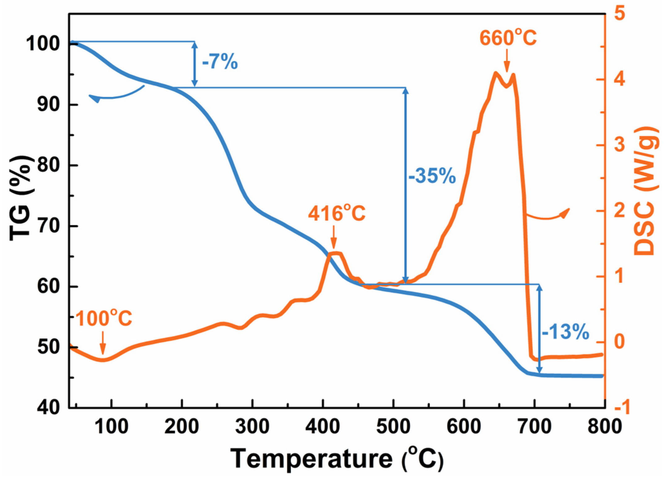
Before the thermogravimetry (TG) and differential scanning calorimetry (DSC) measurements, the BNT–5.5BZ gel was dried at 80 °C on a hot stage. Then, TG and DSC curves were obtained for a dried BNT–5.5BZ gel powder to determine the appropriate annealing conditions, as shown in
Figure 1. Three decomposition steps occurred for a total mass loss of ~55% upon heating from 40 °C to 800 °C in a N
2 atmosphere. The first step, with a mass loss of 7%, took place up to 200 °C due to the evaporation of the absorbed water. Then, a mass loss of 35% occurred near 416 °C, showing an exothermic event. It indicated that the remaining organics and other volatiles were removed around this temperature [
20]. Finally, up to ~660 °C, a 13% mass loss occurred which might be due to the crystallization of the BNT–5.5BZ thin films. During the heating process of the films, the evaporation of water was proceeded at 150 °C, then at 420 °C, the removal of organics and volatiles took place, and last, >650 °C, the nucleation and crystallization of the films occurred. This process is commonly used for the preparation of BNT–based thin films [
7,
8].
The preparation of BNT–5.5BZ thin films was divided into two steps: spin–coating and annealing. All BNT–5.5BZ thin films were deposited on polycrystalline Pt/TiO2/SiO2/Si (001) substrates. First, span–coating proceeded at 3000 revolutions per minute for 40 s. A single wet gel layer was submitted to a heating process: 150 °C for 3 min and 420 °C for 10 min, using a rapid thermal process, leading to the evaporation and removal of the residual organics. Then, two annealing processes were used to form the films. One–step annealing for the single–layer film was conducted at 725 °C for 3 min for nucleation and crystallization. After repeating the spin–coating and annealing processes six times, the BNT–5.5BZ thin films were obtained with the desired thickness (the samples were labeled as “725 °C”). The two–step method for the single–layer film consisted in annealing at 650 °C for 3 min after pyrolyzing according to the TG and DSC results, then repeating the spin–coating and annealing processes for six times. Finally, the films were post–annealed at 725 °C for 30 min in an O2 atmosphere (the samples were labeled as “650 °C + 725 °C”).
2.3. Characterizations
For exploring the weight change and thermal performance of the BNT–5.5BZ thin films, thermogravimetry (TG) and differential scanning calorimetry (DSC, STA449F5 Jupiter, NETZSCH, Waldkraiburg, Bayern, Germany) were performed from 40 °C to 800 °C on the BNT–5.5BZ thin films in a N2 atmosphere. The samples’ average structure and local structure obtained after annealing under different conditions were used for X–ray diffraction and Raman spectrometry. The instruments used were a high-resolution X–ray diffractometer (XRD, Empyrean, PANalytical, Almelo, The Netherlands) with Cu Kα1 radiation (λ = 1.5406 Å) and a Raman spectrometer (LabRAM HR Evolution, Horiba, Montpellier, France) with a 532 nm laser. For the surface and cross–sectional morphologies of the BNT–5.5BZ thin films, pictures were taken by a scanning electron microscope (Gemini SEM 500, Carl Zeiss, Jena, Germany). For the electrical measurements (such as dielectric, ferroelectric, strain response, and so on), electrodes on the surface of the samples were necessary. Gold electrodes (φ = 300 μm) were prepared by a direct current (DC) sputtering. The frequency and temperature dependence of dielectric constant and dielectric loss of the BNT–5.5BZ thin films were determined by a precision impedance analyzer (E4980a, Agilent Technologies Inc., Santa Clara, CA, USA). The leakage current densities under different electric fields were ensured using a semiconductor characterization system (4200-SCS, Keithley Instruments Inc., Cleveland, OH, USA). The polarization (P) and strain response as a function of the electrical fields (E) (P–E and S–E hysteresis loops) were characterized using a ferroelectric analyzer (TF analyzer 2000, aixACCT, Aachen, Germany) with a double–beam laser interferometer (aixDBLI, aixACCT, Aachen, Germany). The out–of–plane displacement–voltage hysteresis loops and phase–voltage hysteresis loops of the BNT–5.5BZ samples were obtained by a scanning force microscope (Dimension Icon, Bruker, Billerica, MA, USA) in piezoresponse force microscopy (PFM) mode with a conductive tip (DDESP, resonant frequency ~450 kHz, spring constant = 80 N, Bruker, Billerica, MA, USA).
3. Results and Discussion
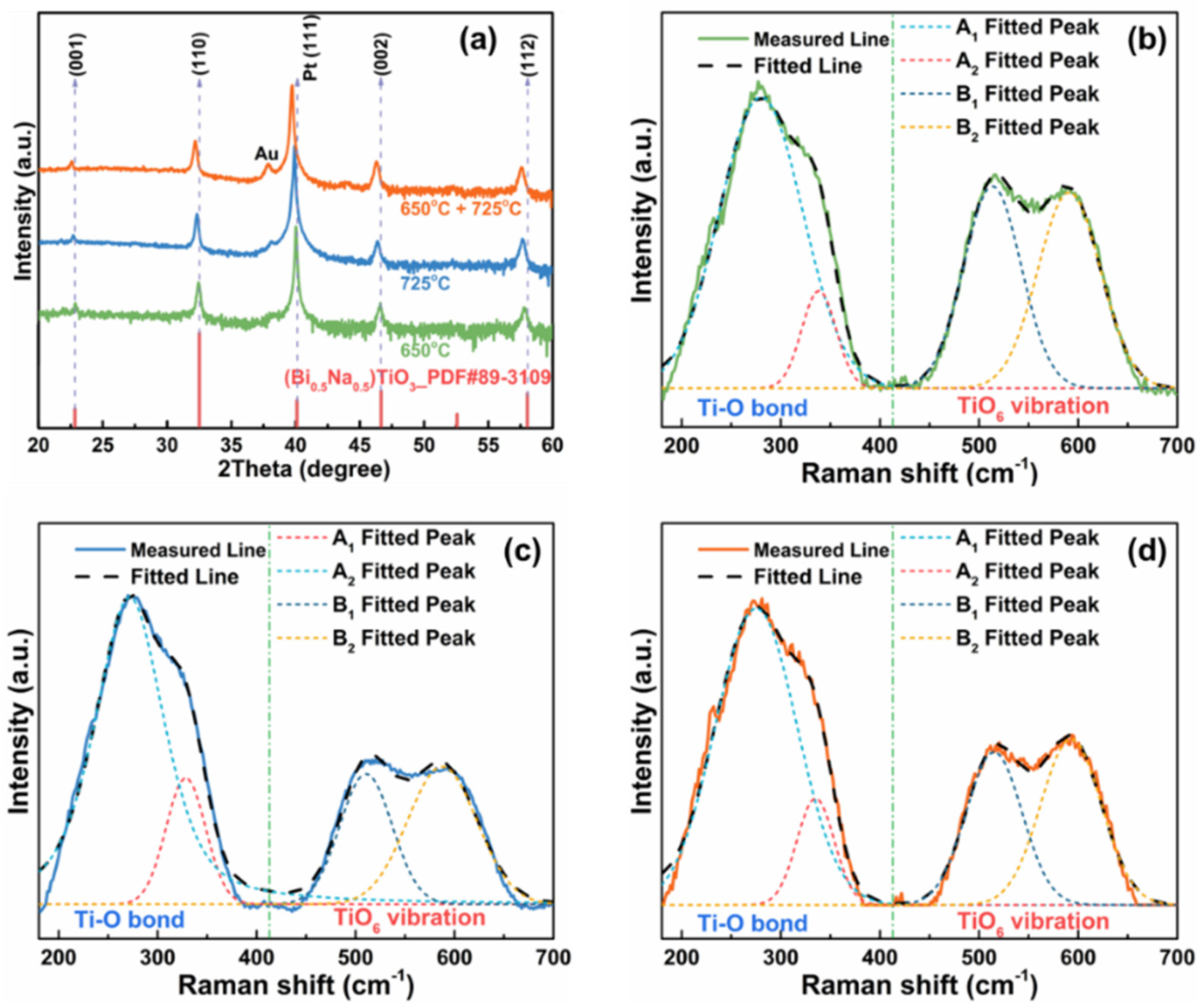
Figure 2a shows the X–ray diffraction results from 20° to 60° of the BNT–5.5BZ thin films annealed under different conditions. There are five independent diffraction peaks in this 2
θ range, as shown in
Figure 2a. Except for the intense Pt (111) peaks near 39.7° and the weak Au (111) peaks (top and bottom electrodes) near 37.9°, the four independent diffraction peaks correspond to (001), (110), (002), and (112) of a single phase of perovskite structure for the BNT–5.5BZ thin films. Unlike preferred oriented films, the BNT–5.5BZ thin films in this work possessed a polycrystalline structure characterized by four diffraction peaks. In addition, all the samples annealed in different conditions presented a similar single-phase structure without any secondary phase. The BNT–5.5BZ thin films were well crystallized at an annealing temperature exceeding 650 °C, following the crystallization temperature from the TG and DSC curves in
Figure 1. The X–ray diffraction peaks of all BNT–5.5BZ samples in
Figure 2a shifted to a lower 2
θ angle, due to of Ba
2+, Zr
4+, with the large atomic radii, replacing Bi
3+, Na
+, and Ti
4+, with small atomic radii [
8], compared with those of pure BNT. Furthermore, this shift was more evident for the “650 °C + 725 °C” films, indicating that the post–annealing treatment of the BNT–5.5BZ thin films promoted the diffusion of the BZ component into the BNT lattice and enhanced the crystallization. To further study the local structure of the BNT–5.5BZ thin films, Raman spectra were collected at RT, as presented in
Figure 2b–d. The spectral deconvoluted results of the BNT–5.5BZ thin films were obtained according to Gaussian–Lorentzian modes [
21]. Four different fitted peaks (A
1, A
2, B
1, and B
2) are shown, while the corresponding locations of the fitted peaks are marked in
Figure 2b–d. Two main vibration regions are present for all BNT–5.5BZ thin films in
Figure 2b–d. One (Region A) is the vibrations of the Ti–O mode in the range of 180 cm
−1–400 cm
−1, and the other (Region B) is the vibration of the TiO
6 octahedra in the range of 450 cm
−1–700 cm
−1 [
22,
23]. In Region A, the locations of the fitted A
1 and A
2 peaks shift simultaneously to lower frequencies as shown in
Figure 2b–d, while the fitted B
1 and B
2 peaks in Region B shift simultaneously to higher frequencies, indicating that the post–annealing treatment played a noticeable effect on the local structure of the BNT–5.5BZ thin films. In our previous work, the Raman fitted results exhibited a similar tendency as the XRD diffraction peaks to shift to a lower 2
θ angle. These results, combining the XRD patterns and the Raman results, suggest that the post–annealing treatment of the BNT–5.5BZ samples promoted the BZ component diffusion in the BNT matrix.
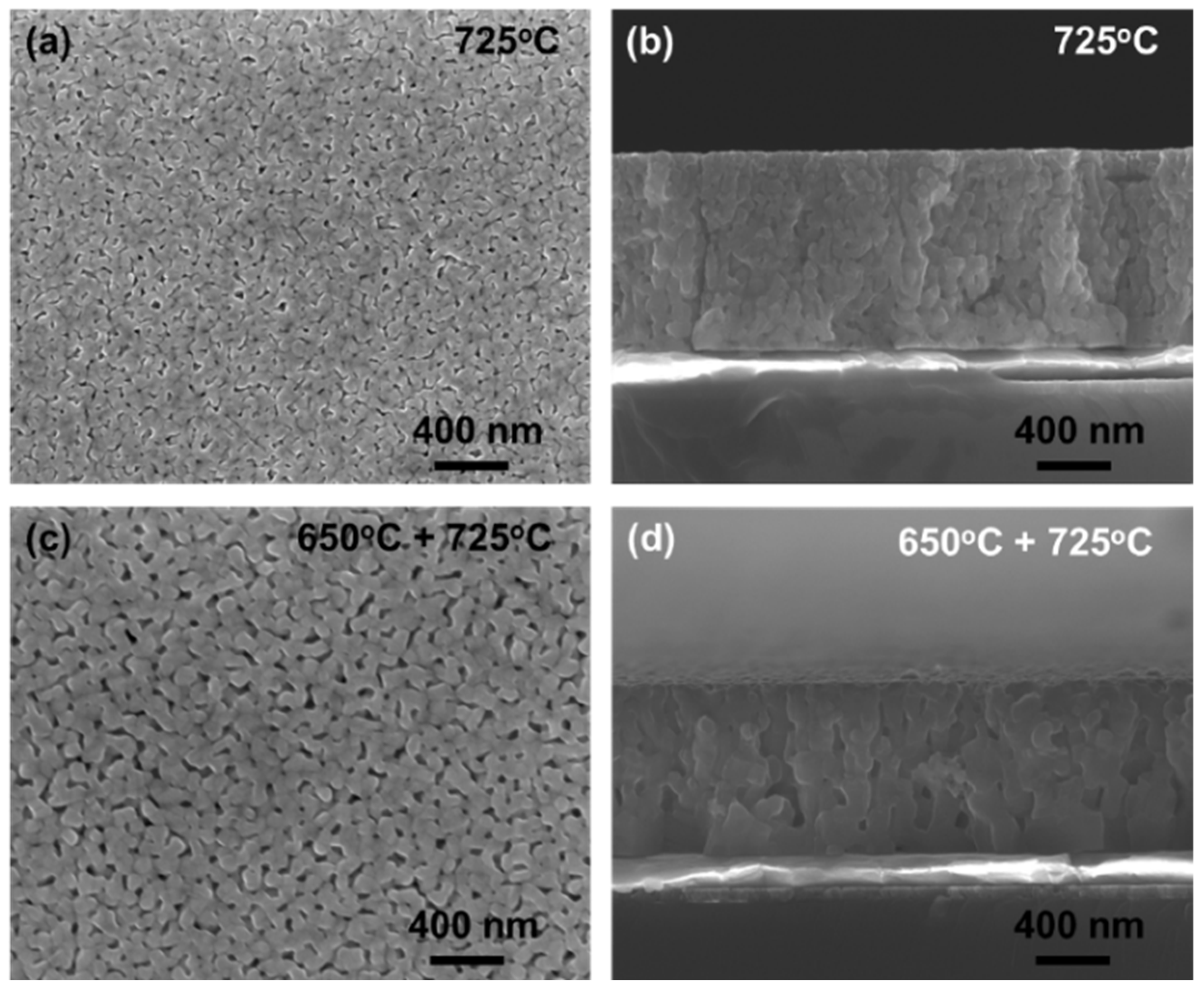
The top-view SEM images of the BNT–5.5BZ thin films annealed in different conditions are shown in
Figure 3a,c. It is obvious that the grain size of the “650 °C + 725 °C” films was larger than that of the “725 °C” films. After post–annealing, the holes decrease, and the grains grow for the BNT–5.5BZ thin films, as displayed in
Figure 3c. The cross–sectional SEM images in
Figure 3b,d present a dense multilayer structure consisting of the BNT–5.5BZ thin film, the bottom Pt/TiO
2 electrode, and the SiO
2/Si substrate, from the top to the bottom of the pictures. A dense columnar growth with an evident interface between the BNT–5.5BZ films and the Pt/TiO
2/SiO
2/Si (001) substrates was present in both films, as shown in
Figure 3b,d. In addition, the thicknesses of the BNT–5.5BZ thin films were calculated to be 0.9 μm–1 μm from the cross–sectional SEM images. An increased grain size in the dense structure of the “650 °C + 725 °C” films annealed in the O
2 atmosphere is more beneficial to enhance the electrical properties.
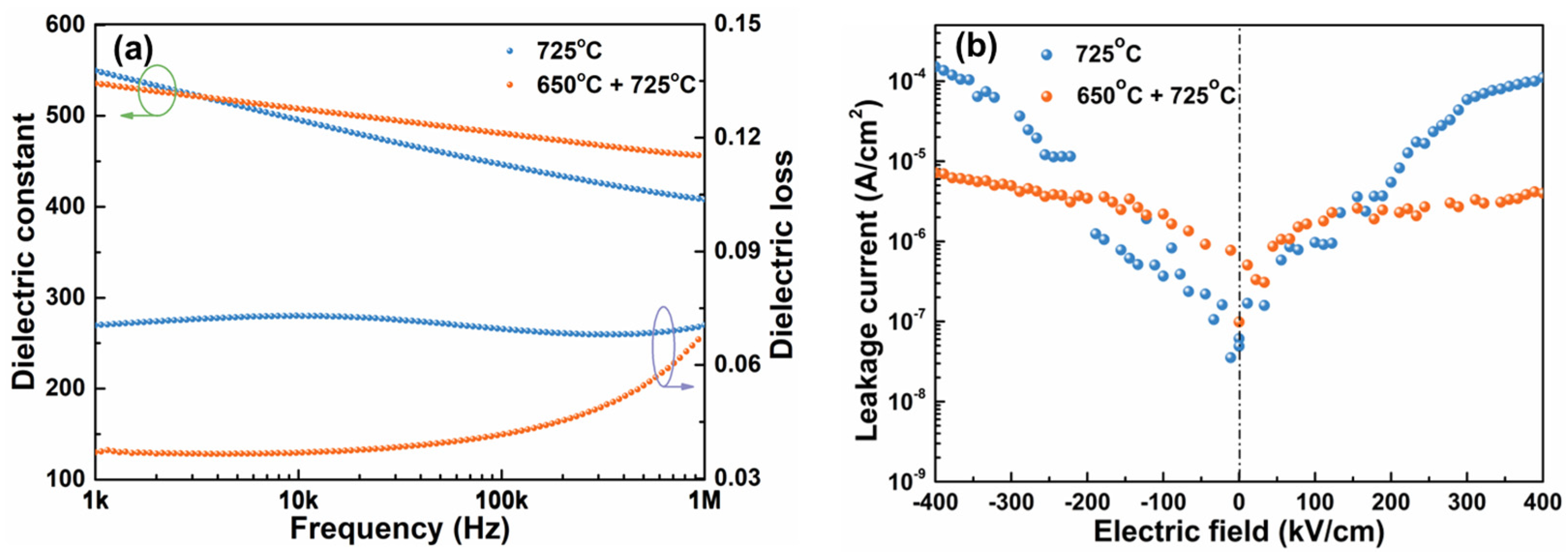
Figure 4a displays the frequency dependence of the dielectric properties from 1 kHz to 1 MHz of the BNT–5.5BZ thin films. An obvious feature of frequency dispersion was exhibited by all BNT–5.5BZ samples: the dielectric constant gradually decreased, while the dielectric loss increased with the frequency increase. This phenomenon could be due to the relaxation of the dipoles, space charge polarization, and so on, similar to what observed for other BNT–based thin films [
7,
8]. The “650 °C + 725 °C” films showed a higher dielectric constant and a lower loss than the other samples at the same frequency from 1 kHz to 1 MHz. Furthermore, the lower dielectric loss of ~0.03 at 1 kHz for the “650 °C + 725 °C” thin films, is much better than those of other works reported in the literature [
24,
25]. The DC electric field dependence of the leakage current for the BNT–5.5BZ thin films is presented in
Figure 4b. It was found that the “650 °C + 725 °C” films exhibited a lower DC leakage current at 0.4 MV/cm compared to the other films. The lower dielectric loss coincided nicely with a low leakage due to the dense and homogeneous structure of the high–quality thin films after annealing. This indicated that the post–annealing process in the O
2 atmosphere for the BNT–5.5BZ thin films likely promoted grain growth and decreased the defects inside the films.
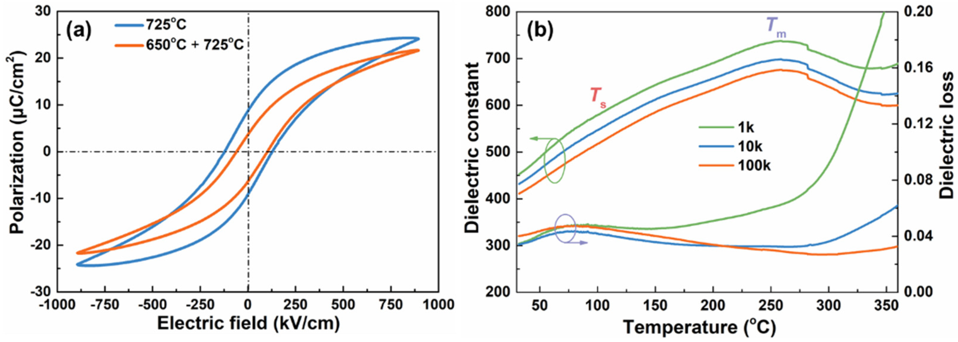
The ferroelectric hysteresis (
P–
E) loops at 0.9 MV/cm for the BNT–5.5BZ thin films are shown in
Figure 5a. A “square–shaped”
P–
E loop was observed for all BNT–5.5BZ thin films, indicating a typical character of ferroelectric materials [
26]. Both maximum polarization (
Pmax) and remanent polarization (
Pr) of the “725 °C” thin films were larger compared with those of the “650 °C + 725 °C” thin films. However, the
P–
E loop of “725 °C” thin films was not completely saturated due to a high dielectric loss and a large DC leakage current (
Figure 4). It was found that the
P–
E loop of the “650 °C + 725 °C” thin films was slimmer and better saturated than those of other BNT–based thin films [
27,
28].
Figure 5b presents the dielectric constant and dielectric loss of the “650 °C + 725 °C” thin films as a function of temperature at the three different frequencies. Two dielectric anomalies of the “650 °C + 725 °C” thin films are observed in
Figure 5b. The first anomaly, similar to a hump or a shoulder, was detected between 80 °C to 180 °C. An evident frequency dispersion around the characteristic temperature
Ts showed a typical ferroelectric relaxor feature [
8,
29]. As the temperature increased, the other dielectric anomaly appeared in the temperature range of 220 °C to 300 °C. The temperature corresponding to the maximum dielectric constant is characterized as
Tm. From the perspective of dielectric behavior, the “650 °C + 725 °C” thin films exhibited the coexistence of a ferroelectric phase and a relaxor state, similar to previously reported BNT–5.5BZ ceramics [
19].
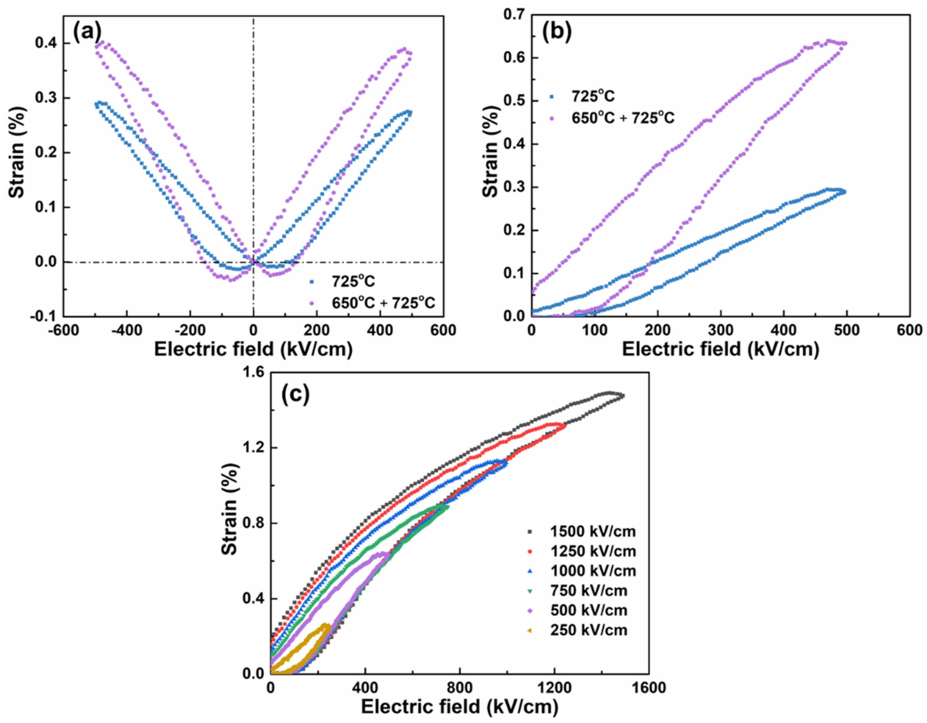
The bipolar and unipolar strain hysteresis (
S–
E) loops at 0.5 MV/cm of the BNT–5.5BZ thin films annealed under different conditions are presented in
Figure 6. “Butterfly–shaped” bipolar
S–
E loops are observed for all BNT–5.5BZ thin films in
Figure 6a, suggesting a typical ferroelectric feature. The “650 °C + 725 °C” thin films exhibited a larger bipolar strain value than the “725 °C” thin films, while the “650 °C + 725 °C” thin films showed a larger unipolar strain response, as indicated in
Figure 6b. The unipolar strain of the “650 °C + 725 °C” films reached 0.63% at 0.5 MV/cm, approximately 2.2 times that of the “725 °C” thin films, i.e., 0.28%. To explore the relation of the unipolar strain response with the applied electric fields, unipolar
S–
E loops as a function of electric fields for the “650 °C + 725 °C” samples were determined and are displayed in
Figure 6c. The unipolar strain values of the films annealed under various conditions linearly increased with the increase in the applied electric fields. It was found that an ultra–high strain response of up to 1.5% was obtained at 1.5 MV/cm for the “650 °C + 725 °C” samples, much better than those of BNT–based and non–BNT–based thin films in previous studies [
30,
31,
32,
33]. Furthermore, the withstand electric field (1.5 MV/cm, the maximum external electric field in the
S–
E measurement before breakdown) in the “650 °C + 725 °C” thin films was much higher than that in the “725 °C” thin films (0.5 MV/cm). A high–withstand electric field in the BNT–5.5BZ thin films after two–step annealing is helpful for device applications.
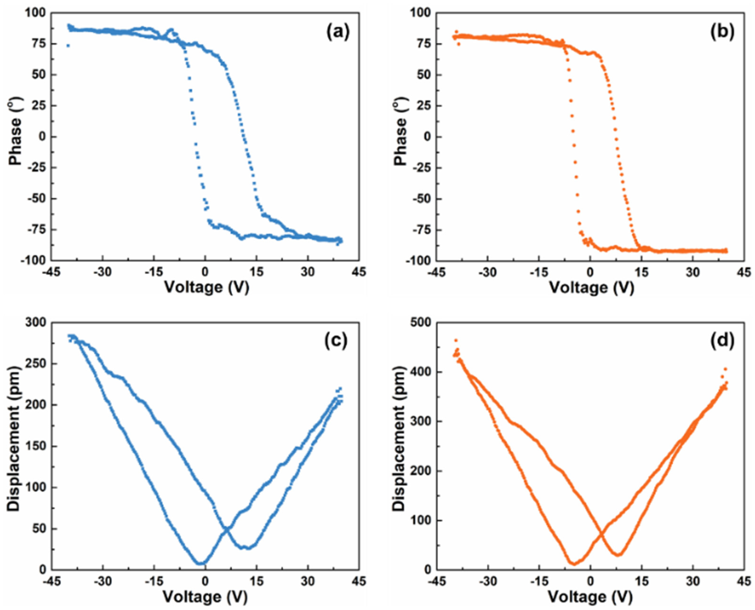
To further study the influence of the annealing conditions on the piezoelectric responses in different dimensions, the local polarization behavior was measured using PFM and is present in
Figure 7. The out–of–plane phase–voltage and displacement–voltage hysteresis loops were determined by applying a dynamical DC bias up to 40 V superimposed on an alternating current (AC) bias (
Vpp = 5000 mV,
f = 280 kHz) on the film surface via the PFM tips. Many researchers have confirmed that the piezoelectric response detected using the PFM method is highly dependent on the PFM measurement conditions, such as laser location, measuring parameters, tip types, tiny contact area, and so on [
7,
8]. Therefore, all BNT–5.5BZ thin films were measured under the same conditions in this work. “Square–shaped” phase hysteresis loops (in
Figure 7a,b) were shown for all BNT–5.5BZ thin films, demonstrating a typical characteristic of the piezoelectric behavior.
Figure 7c,d shows “butterfly–like” displacement loops measured inside an individual grain in all BNT–5.5BZ thin films. The “650 °C + 725 °C” thin films exhibited a more significant displacement value than the “725 °C” thin films, possibly attributed to the crystal lattice extension and distortion inside the individual grains. Furthermore, a pronounced asymmetry can be seen in both phase–voltage and displacement–voltage butterfly hysteresis loops, mainly caused by the built–in electric field and determined by charges and defects during the poling process [
27]. In addition, the unsymmetrical configuration of the different types of Au top and Pt bottom electrodes in the films cannot be neglected. As a result, a higher micro–scale piezoelectric response was obtained in the films after annealing.
After annealing, an enhanced unipolar strain of ~1.5% and a reduced dielectric loss of ~0.03 were exhibited in the BNT–5.5BZ thin films. It indicated that the post–annealing treatment in the O
2 atmosphere played an essential role in improving the strain responses for the BNT–5.5BZ thin films. A primary crystallization was present in the samples annealing at 650 °C, as shown by the XRD and Raman results. However, when post–annealed at 725 °C in an O
2 atmosphere, the films might exhibit a complete crystallization with a large grain size. For BNT–based ceramics, the strain response strongly depends on the grain size. The strain response can be improved by increasing the grain size for ceramics with a dense structure [
34]. The grain size growth in the BNT–5.5BZ films after the annealing treatment made it possible to achieve a much larger micro–scale polarization response (
Figure 7) compared to the non–annealed samples. Post–annealing treatments are commonly used to reduce the oxygen vacancies and release residual stresses both on surfaces and inside films [
35]. Furthermore, oxygen interacts with oxygen vacancies in the films, increasing the grain size when annealing the films at high temperatures in an O
2 atmosphere [
17]. In this work, the post–annealing in an O
2 atmosphere for the BNT–5.5BZ thin films could effectively decrease defects due to the volatility of alkali metal elements during the heating process. The appearance of oxygen vacancies could be inhibited in this process, and an improvement of the grain size was achieved, as shown in the top–view microstructure due to the increased annealing time [
36]. The BNT–5.5BZ thin films presented the coexistence of the ferroelectric phase and the relaxor state, as shown by their dielectric behaviors under different temperatures in
Figure 5b. As studied in our previous works [
8,
37], a significant strain response is easier to realize near the ferroelectric and relaxor phase boundary thanks to a reversible field–induced phase transition [
38]. Therefore, post–annealing in an O
2 atmosphere effectively optimized the quality and strain responses of the BNT–based thin films.


