Article

Enhancement of Thermoelectric Performance for InTe by Selective Substitution and Grain Size Modulation

1
School of Physics and Optoelectronic Engineering, Yangtze University, Jingzhou 434023, China
2
Shenzhen Institute of Advanced Electronic Materials, Shenzhen Institute of Advanced Technology, Chinese Academy of Sciences, Shenzhen 518055, China
*
Authors to whom correspondence should be addressed.
Crystals 2023, 13(4), 601; https://doi.org/10.3390/cryst13040601
Submission received: 9 March 2023 / Revised: 25 March 2023 / Accepted: 29 March 2023 / Published: 1 April 2023
(This article belongs to the Special Issue Advanced Electronic Materials and Devices)

Abstract

:
The different masses, ionic radii, and chemical valences of the nonequivalent crystallographic sites of thermoelectric (TE) compounds provide an effective way to modulate the thermoelectric performance by selective substitution. In this work, the selective substitution of In+ by Pb for the binary InTe material monotonically reduces the carrier concentration, which is greatly beneficial to the mechanism investigation of serious grain boundary scattering (GBS). This is the first time this point has been mentioned with regard to InTe material. As a result, we found that GBS was dominated by the grain size when the carrier concentration was higher than 0.7 × 1019 cm−3 but was inversely governed by the carrier concentration when the carrier was situated at a lower density. In particular, the occupation of Pb on the targeted In+ site could further reduce the lattice thermal conductivity. Finally, In0.9999Pb0.0001Te achieved the improved power factor and average zT value, which could contribute to high-power generation below a medium temperature. This effect of increasing the carrier concentration on the suppression of GBS sheds light on the possibility of improving electron mobility by increasing the carrier concentration.

1. Introduction

Thermoelectric (TE) materials have the ability to create direct conversion between heat and electricity without any moving parts or noise; they are regarded as eco-friendly energy materials and have attracted intensive attention in the scientific community [1,2,3]. The heat-to-power conversion efficiency (η) is strongly related to the materials’ dimensionless figure of merit, zT = S2σT/(κL + κe), where T, σ, S, κL, and κe are the absolute temperature, electrical conductivity, Seebeck coefficient, lattice, and electron thermal conductivity [4]. The strong coupling of S, σ, and κe through carrier concentration makes it extremely difficult to improve the zT value. Thus, it requires the band engineering of degeneracy [5,6], curvature [7], and valley anisotropy to improve the electronic performance as well as microstructural defect engineering to reduce the independent κL in order to increase the thermoelectric performance [8,9,10,11]. In addition, the exploration of new materials with low κL provides an effective way to achieve outstanding TE properties [9,10,12,13,14,15,16,17].
The new rising binary InTe possesses a typical characteristic of phonon-glass electron-crystal (PGEC) [18,19]. It features a TlSe-type structure with one directional (1D) strong covalent chains of [In3+Te4/22−] along a c direction, which are further weakly bridged by an In+ cation with 5s2 lone pair electrons [20]. The weak ionic bonds result in the large anharmonic vibrations of In+ and the strong anharmonic phono–phonon interactions, which induce an extremely low κL even for the single crystal of InTe. In recent years, the high TE performance has been obtained by atomic doping and single crystal growth [16,21,22,23,24,25,26,27], which promotes the peak zT high up to 1.2 @648 K [15]. Compared with the varied doping results of Cu, Na [27], Cd [23], Sb [22], Pb [21], Ga [15], etc., Pb:InTe achieved the lowest lattice thermal conductivity, which was derived from the anharmonic vibrations of In+ and the selective doping at the In+ site for the different ionic radii ( r I n + > r P b 2 + > r I n 3 + ).
On the other hand, lattice thermal conductivity is totally governed by specific heat CV, phonon group velocity v, and the mean free path of the heat-carrying phonon, i.e., κ L = C V vl . The inherently anharmonic vibrations have generated a low v and κL for InTe. In addition, the l can also be modulated to further reduce the κL since it mainly depends on the phonon scattering mechanism, such as phonon–phonon scattering, microstructural defect scattering, and nanoparticle scattering. However, the previous investigation of polycrystalline InTe with varied grain sizes indicated that the reduction in grains actually reduced κL but also caused it to be strongly scattered by the grain boundary (GB) of the carrier, which resulted in low electrical conductivity below ~500 K [15,21,22] and severely deteriorated the TE performance at room temperature. Therefore, how to enhance the phonon scattering but not seriously affect the carriers’ transportation becomes the main purpose for grain size modulation. In principle, GBS is related to the Fermi level, grain size, grain boundary barrier, and so on for materials [15,22], resulting in the strong relationship of the GBS and the carrier concentration. Up to now, how the carrier concentration affects the GBS is rarely mentioned for InTe. Thus, it prompted us to explore the synergistic effect of grain size and carrier concentration on depressing GBS based on varied grain sizes with a monotonic reduction in the carrier concentration.
In this work, we systematically investigated the effects of Pb doping amounts and grain sizes on the modulation of the electron and phonon transports of InTe. In addition, the Pb doping could monotonically reduce the carrier concentration, which provided the opportunity to explore the effect of carrier concentration on the suppression of GBS for InTe. As a result, both grain size and carrier concentration significantly influenced the GBS. The GBS could be depressed by increasing the grain size only when the carrier concentration was larger than 0.7 × 1019 cm−3. In addition, Pb doping also greatly reduced the lattice thermal conductivity. Therefore, the improved zT value below 600 K for Pb0.0001In0.9999Te was obtained, which was beneficial to the power generation below medium temperature. Furthermore, this effect of carrier concentration on the suppression of GBS illustrated the possibility of electron mobility improvement by increasing the carrier concentration.

2. Materials and Methods

In order to synthesize the pure phase of In1-xPbxTe (x = 0, 0.0001, 0.001, 0.003, 0.005), the high-purity (>99.99%) indium, lead, and tellurium particles were weighed in stoichiometric ratios and then loaded into the carbon-coated quartz tubes. The indium, lead, and tellurium particles were produced by Zhongnuo Advanced Material Technology Co., Ltd (Beijing, China). Additionally, due to the very small doping amount of Pb, the total amount in our experiment was >20 g. However, in this situation, for Pb0.0001In0.9999Te the amount of Pb was >2 mg, which could be accurately weighed because the weighing error was only ±0.0005 g. Subsequently, the quartz tubes were sealed with a vacuum of ~10−1 Pa. The tubes containing In, Te, and Pb were heated to 1123 K in 7 h and then held at this temperature for 4 h before the furnaces were switched off. The obtained InTe ingot was hand-ground and sieved with two particle size ranges of >150 μm (80 mesh) and <50 μm (300 mesh), respectively (marked as InTe-Coarse and InTe-Fine, respectively), and the other ingots of In1−xPbxTe (x = 0.0001, 0.001, 0.003, 0.005) were hand-ground and sieved with only large sizes of >150 μm. Finally, these powders were loaded into graphite dies with an inner diameter of 10 µm, which were placed in the hot-press sintering furnace (NYRH-HP). The sintering was operated under a uniaxial pressure of 50 MPa with a vacuum <5 Pa at 773 K for 30 min, producing pellets with high densities (>95% of the theoretical densities), which were then cut into small samples with dimensions of 10 × 2 × 2 mm3 and 6 × 6 × 1.5 mm3 for measurements of the electrical and thermal properties. It needs to be mentioned that the electrical and the thermal conductivity were measured along the pressure direction due to the anisotropic atomic structure of InTe and the high texture degree of the (110) along this direction.
The phase purity of the samples was confirmed by powder X-ray diffraction (PXRD) using a Bruker AXSD8 Adance X diffractometer (Saarbrücken, Germany) with Cu Kα radiation of 1.5406 Å at room temperature. A scanning electron microscope (Thermo Scientific Apreo 2 S HiVac, 5 kV, Waltham, America) equipped with an energy-dispersive X-ray spectrometer (EDS, Waltham, America) was used to investigate the microstructures and chemical compositions. The electrical conductivity and Seebeck coefficient were measured using an Ulvac ZEM-3 (Chigasaki, Japan) from 300 K to 773 K, based on the same sample. The thermal diffusivity (D) was measured between 300 K and 773 K by using the laser flash diffusivity technique on an LFA-467 instrument (Netzsch, Selb, Germany). The total thermal conductivity was calculated using the relation of κ = DCpρ, where ρ is the density of the sample measured by the Archimedes method, and Cp is the specific heat capacity using the Dulong–Petit estimation, due to the low Debye temperature of around 200 K [22]. The Hall coefficients (RH) were measured by the van der Pauw technique with a Xiangjin self-made Hall electrical performance test system (NYMS) under a helium atmosphere. The Hall carrier concentrations (nH) and Hall mobilities (μH) were estimated by nH = 1/eRH and mH = sRH, respectively.

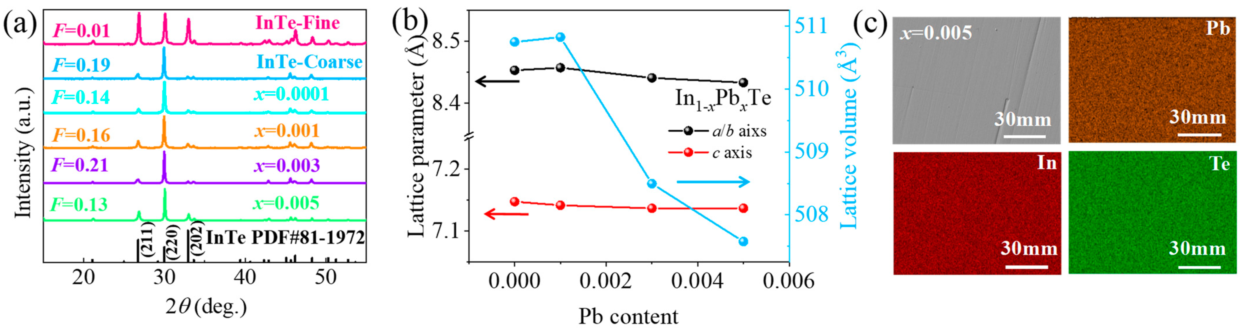
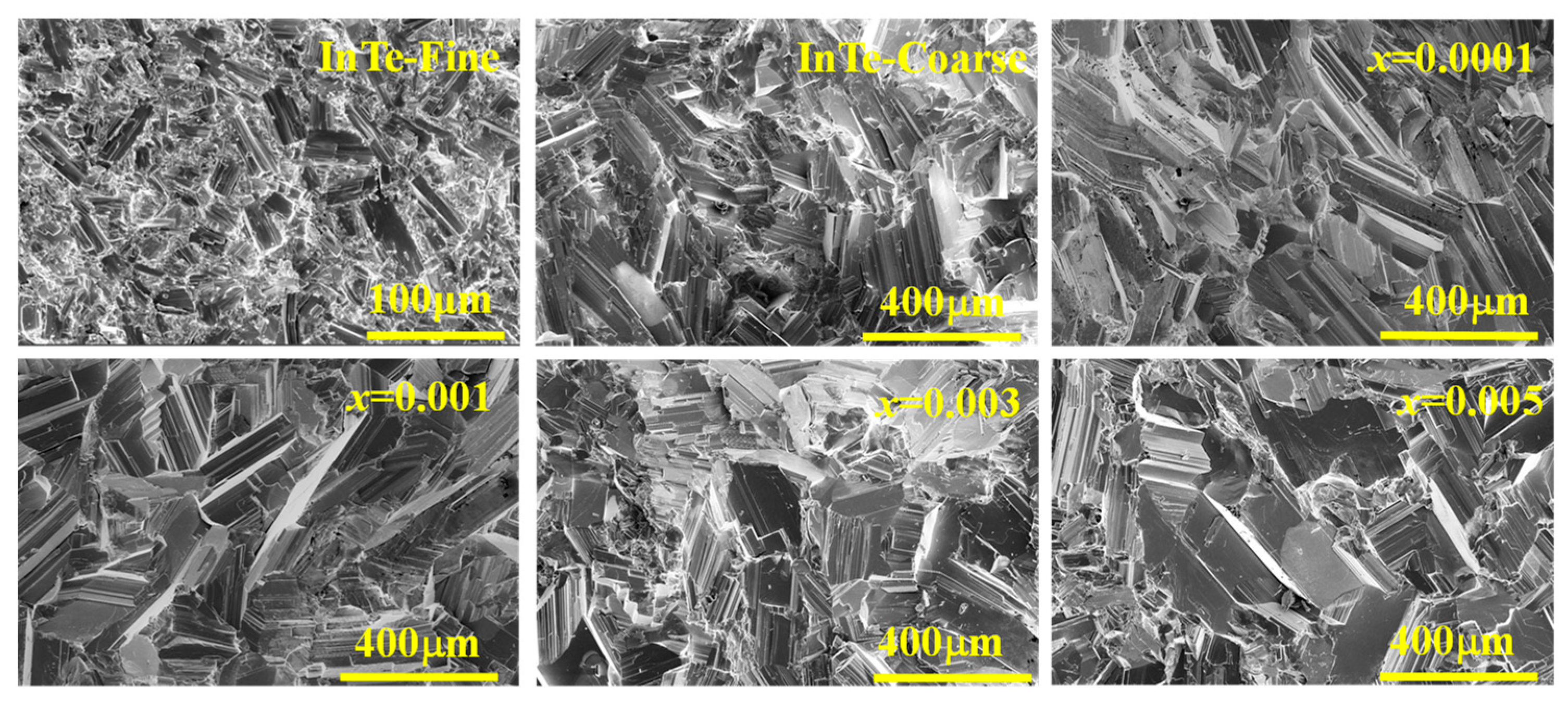
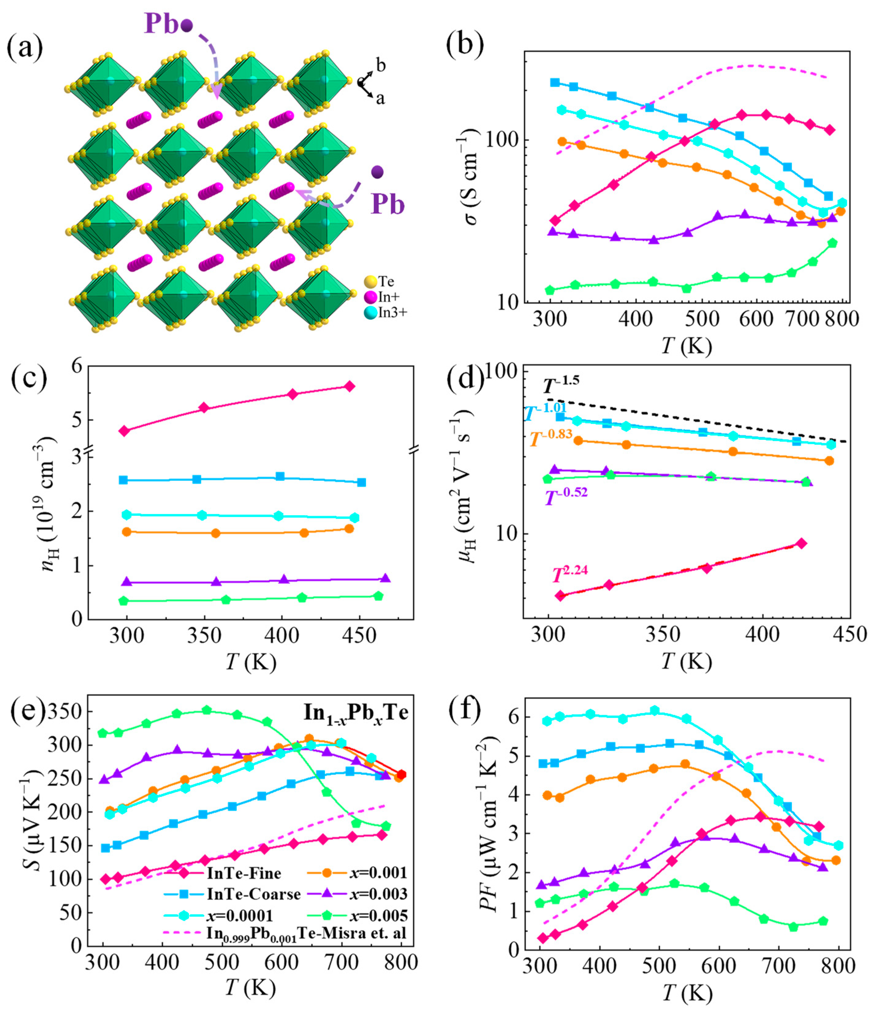
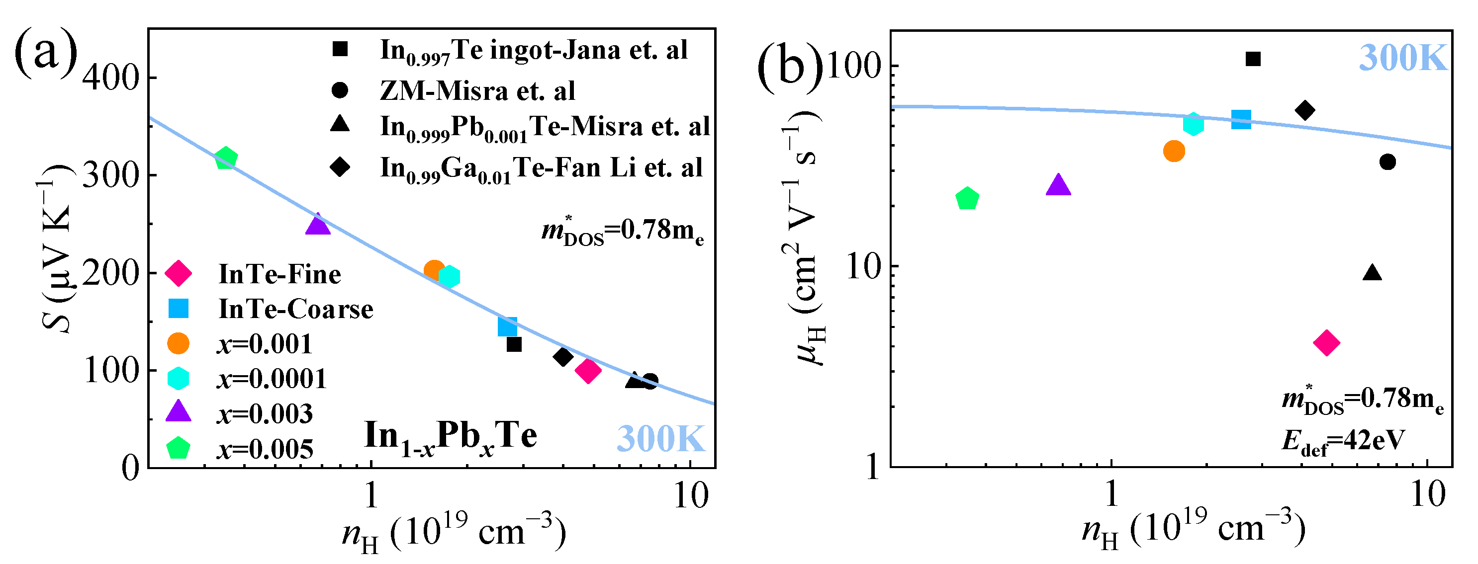
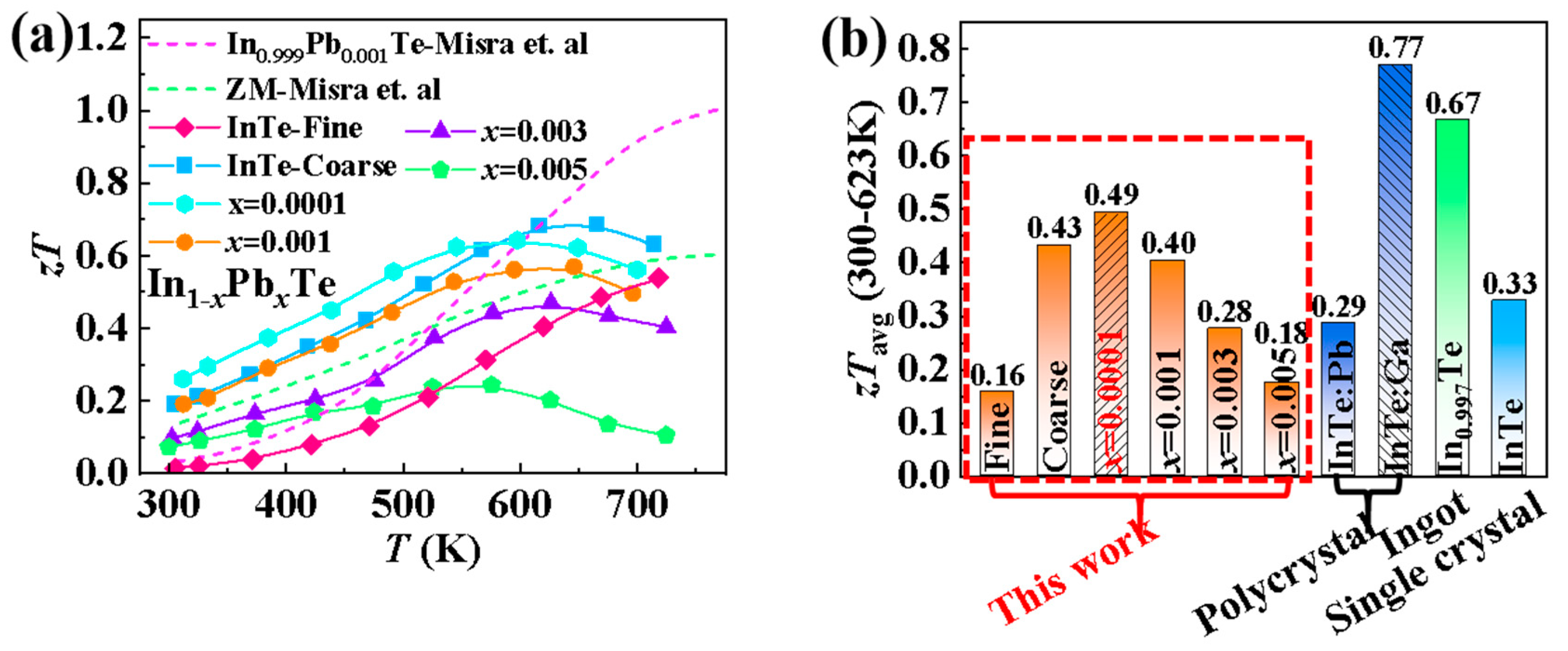
3. Results and Discussion

The obtained samples of In1-xPbxTe (x = 0, 0.0001, 0.001, 0.003, 0.005) showed high phase purity, which could be verified by the good agreement of their PXRD pattern positions with the standard JCPDS card (PDF#81-1972) of the InTe, as shown in Figure 1a. However, the different intensities of the PXRD peaks for the samples revealed their varied texture degrees. In detail, through the grain size modulation, the texture degree of the (ll0) plane could be increased from 0.01 to > 0.1, which was calculated by the formula:
F = P P 0 1 P 0 ,   P 0 = I 0 00 l Σ I 0 hkl ,   P = I 00 l Σ I hkl
where I(hkl) and I0(hkl) are the peak integral intensities for the measured and randomly oriented samples, respectively [28]. In addition, the Pb-doped samples with large grain sizes also had the large orientation factor F(ll0), which was similar to that of the coarse pure polycrystalline InTe. This improved texture degree was highly beneficial to the utilization of the expected anisotropic transports of higher electrical conductivity and lower thermal conductivity along the [110] direction; this was confirmed by the investigation of the transports based on a single InTe crystal and could be taken advantage of to improve the TE performance of InTe [29]. Furthermore, the cell parameters were refined based on the XRD data, and the results are shown Figure 1b. It can be seen that the lattice gradually decreases with the increase in the Pb doping concentration, which is consistent with our experimental design with regard to the substitution of In+ by Pb2+ ions, because of their different ionic radii r I n + > r P b 2 + > r I n 3 + . In addition, the pure phases can also be confirmed by the uniform distribution of the elements, which can be seen from the EDS results presented in Figure 1c because there is no second phase that can be observed.
The SEM results are displayed in Figure 2, which clearly shows that the average grain sizes of the sieved coarse In1-xPbxTe (x = 0, 0.0001, 0.001, 0.003, 0.005) are larger than 150 µm, and this value is much larger than that of InTe-Fine (<50 µm). According to the previous studies, the large grain sizes are beneficial to the depression of the GBS of InTe and can be expected to considerably improve the carrier mobility below 500 K [15,30,31]. Therefore, the samples with large grains can remove the influence of the grain size when analyzing the relation of the carrier concentration and the GBS in this work.
Figure 3 displays the electrical performance of the In1-xPbxTe (x = 0, 0.0001, 0.001, 0.003, 0.005) samples. As shown in Figure 3b, the σ reduces with the rising Pb doping ratio. In terms of the crystal structure, the In atom has two independent crystallographic sites of In+ and In3+, and the In+ cation with 5s2 lone pair electrons has a larger size than the In3+ cation. Considering the large difference in the ionic radii of In+ (1.32 Å), In3+ (0.81 Å), and Pb2+ (1.19 Å) [32,33], Pb2+ prefers to replace In+ to locate between the covalent chains, which can reduce the carrier concentrations, as displayed in Figure 3a,c, and can give rise to the reduction in the σ with the increase in the doping amount, as shown in Figure 3b. This result is consistent with the reduced cell parameters resulting from the increasing of the doping ratio.
It should be noted that the temperature-dependent conductivity shows greatly different trends for In1-xPbxTe (x = 0, 0.0001, 0.001, 0.003, 0.005) with the varied carrier concentration. As shown in Figure 3b, the temperature-dependent electrical conductivity of coarse InTe presents a monotonically decreased trend which is similar to that of the single crystal due to the depression of GBS [29]. Although they have the smaller n, the σ of coarse InTe and Pb0.0001In0.9999Te at room temperature are definitely much higher than those of the samples with fine grains [21]. These results are consistent with those in the literature on depressing GBS by increasing the grain size. However, when the carrier concentration is reduced, the electrical conductivity trend changes from a monotonic decrease to one which first rises then falls, even with samples with coarse grains. This situation has not been observed in other works of InTe. In order to analyze the mechanism of carrier scattering in detail, the carrier mobility was calculated based on the temperature-dependent carrier concentration, as shown in Figure 3d. When the doping ratio is lower than 0.1%, the μH shows the temperature-dependent behaviors of T−1.04 for x = 0.0001 and T−0.89 for x = 0.001 within 300–423 K (Figure 3d), which is close to the acoustic phonon scattering (APS) relation of T−1.5. However, the μH shows a T0.52 relation when the doping ratio is higher than 0.3% and the nH is smaller than 0.7 × 1019 cm−3, indicating the strengthened GBS and weakened APS when the carrier concentration is reduced.
Academically, the GBS is related to the potential barrier (Eb) of the GB based on the trapping state model [34,35,36], which is expressed as:
E b = e 2 d 2 N 8 ε d N < Q t e 2 Q t 8 N ε   d N > Q t
where d is the grain size, e is the elementary charge (C), ε is the dielectric constant, Qt is the density of the trapping states at the grain boundaries (C m−2), and N is originally defined as the concentration of ionized impurity atoms for the intrinsic semiconductor (usually dopant atoms, m−3), which reflects the carrier concentration. Therefore, the Eb of the TE material largely depends on the carrier concentration and the grain size. Generally, there are three different situations in which to estimate the Eb: (1) when the carrier concentration is high enough, the Eb could be very weak and can be ignored regardless of whether the grain size is large or small, which has been verified in other materials with high carrier concentration; (2) for TE materials with a normal carrier concentration, merely growing the grain size can reduce the Qt and then depress the Eb and GBS, which is commonly used to remove the GBS of TE materials [31,37,38]; and (3) when the grain size is large enough, reducing the carrier concentration can still elevate the Eb and then promote the GBS, which is merely mentioned in electrical transport [30,39]. In this work, even for the coarse polycrystalline InTe, when raising the Pb doping ratio higher than 0.3%, the decreased nH contributes to the increase in Eb and magnifies the GBS effect. The increase in carrier concentration to suppress the GBS illustrates the possibility of improving electron mobility by increasing the carrier concentration.
The positive Seebeck coefficients of all the samples reveal their p-type transports, as displayed in Figure 3e. With the doping ratio increasing, the room temperature S monotonically enhances due to the reduction in carrier concentration. It is interesting that the Seebeck coefficients are approached even with the different doping ratios at high temperature; this originates from the different intensity of the bipolar transports resulting from the thermal activation of the samples. This can also be reflected in their different band gaps (Eg) because the Eg of the samples decrease from 0.42 eV to 0.33 eV with the increase in the Pb doping amount, according to the calculation based on the Seebeck coefficient in the following formula [40]:
Eg = 2eSmaxT(Smax)
where Smax and T(Smax) are the peak Seebeck coefficient and the corresponding temperature, respectively. Specifically, the reduced Eg lowers the thermal activation temperature of the electron, and these thermally excited electrons reduce the S significantly at the high temperature due to the involvement of two kinds of carrier, which is expressed as [40]:
S = S n σ n + S p σ p σ n + σ p
where Sn, Sp, sn, and sp are the Seebeck coefficient and the electrical conductivity for the electron (n) or hole (p), respectively. Therefore, a suitable band gap is important for the thermoelectric material to achieve high a Seebeck coefficient. Finally, the improved S of In0.9999Pb0.0001Te and the high σ give rise to the 20% increment of the power factor (PF) near room temperature, as shown in Figure 3f. However, with the increasing doping amount of Pb, the PF will monotonically reduce because of the reduction in σ, which originates from the low carrier concentration and the strengthened GBS.
The single parabolic band (SPB) model, which is applicable under the condition of the acoustic phonon dominating the carrier scattering, is used to study the S-nH and μH-nH relationship and predict the optimal nH to achieve the highest electrical performance in this work [15,41]. At room temperature, the S-nH relation fits well the SPB Pisarenko curves (i.e., S vs. nH), with the density-of-states effective mass (m*DOS) of 0.78 me (Figure 4a), which is close to those of coarse grain-In0.99Ga0.01Te [15], In0.999Pb0.001Te [21], InTe ingot [16], and InTe single crystal [29]. For InTe, there are complex carrier scattering mechanisms, including GBS, APS, and point defect scattering (DPS), as well as intervalley scattering and ionized impurity scattering [15,22,25,26]. However, it seems that the mixed scattering mechanism does not affect the Seebeck coefficient trend significantly. However, the μH is strongly related to the scattering mechanisms; this means that μH will increase with the elimination of GBS, which can be illustrated by the μH-nH relation, as shown in Figure 4b. Therefore, removing the GBS can significantly increase the electrical properties.
The sieved coarse In1-xPbxTe (x = 0, 0.0001, 0.001, 0.003, 0.005) with a high texture degree of the (ll0) plane can utilize the extraordinarily low thermal conductivity of InTe along the [110] direction. In addition, the doping of the heavy atom Pb can further introduce the point defect to reduce the lattice thermal conductivity (κL) and thus produce extremely low total thermal conductivity (κtotal), as shown in Figure 5a. At room temperature, the κtotal tonelessly decreased with the increase in the doping amount due to the intensified point defect derived from the fluctuations of the atomic mass and radius. In addition, the κtotal of all the samples normally decreased with the increase in temperature below 500 K for the increased phonon–phonon scattering as the temperature increased. However, the κtotal for the doped samples showed a slight upturn when the temperature was higher than 500 K, indicating the contribution of the bipolar diffusion and the recombination, which was analyzed above. In order to evaluate the intrinsic κL, the electron thermal conductivity (κe) was first calculated according to the Wiedemann–Franz law and is expressed as [42]:
κe = LσT, L = 1.5 + exp [−|S|/116]
where L is the Lorenz number, σ is the electrical conductivity, and T is the absolute temperature. The L can be estimated from the experimental Seebeck coefficient. Being consistent with the electrical conductivity, κe reduces with the increase in the doping ratio, as shown in Figure 5b. As noted in the Debye model, the dominant Umklapp scattering indicates that κL and T obey the relation of κL = aT−1 + b above the Debye temperature [43,44]. Thus, the lattice thermal conductivity was first estimated by subtracting κe from κtotal within 300–400 K and then extrapolated in the subsequent temperature range, as shown in Figure 5c. It is clear that, with increased Pb doping, κL can be reduced by 23% at 300 K to 0.49 Wm−1 K−1 and by 16% at 700 K to 0.30 Wm−1 K−1, which is lower than the limit of κglass ~ 0.32 Wm−1 K−1 with the Cahill model [45] and close to the limit of κdiff ~ 0.21 Wm−1 K−1 with the diffusion model [46]. The traditional Cahill model is expressed as:
κ glass 1.21 n 2 / 3 k B 1 3 2 v t + v l
where n is the number density of the atoms, kB is the Boltzmann constant, vt is the transverse sound velocity, and vl is the longitudinal sound velocity. In addition, the κb of each sample was calculated with the expression κb = κtotalκeκL, as shown in Figure 5d; this reveals the increased contribution of κb with the increase in the temperature and doping amount. Therefore, in order to obtain a high thermal conductivity of the thermoelectric material at high temperature, a suitably large band gap is necessary in order to avoid the powerful influence of bipolar diffusion.
The calculated zT values of all the samples, based on the measured electrical and thermal properties, are presented in Figure 6. Due to the simultaneously optimized electrical and thermal conductivity, the zT value increased from 0.02 for polycrystalline InTe with fine grains to 0.2 for the coarse one and further to 0.26 for In0.9999Pb0.0001Te with coarse grains at room temperature. In addition, the peak zT value can also be increased from 0.54 to 0.70 with the increase in the grains. Because of the depression of GBS when x < 0.3% and the high texture degree of the (110) plane, the average zT of coarse grain-In1-xPbxTe sample can also be increased greatly; this was calculated by the following equation:
z T avg = 300 623 z T ( T ) d T Δ T
In detail, the z T avg increased by 168%, from 0.16 to 0.43, with the increasing grain size and further increased by 14% to 0.49 with Pb doping. This value is much higher than that of the Pb-doped (0.29) sample with fine grain in the literature and ranks higher among all the reported polycrystalline InTe-based TE materials, as shown in Figure 6b.

4. Conclusions

In summary, in order to fully investigate the mechanism of the grain boundary scattering of InTe, we systematically explored the synergistic effect of grain size and the carrier concentration on the carrier scattering mechanism with selective Pb doping at the In+ site. This design could monotonically reduce the carrier concentration, which provided the opportunity to explore the effect of carrier concentration on the suppression of GBS for InTe. When the carrier concentration was high, the grain size dominated the GBS, and merely increasing the grain sizes could depress the GBS. However, when the carrier concentration was low (<0.7 × 1019 cm−3) the GBS was still strong even for the coarse polycrystalline InTe. In addition, the Pb doping monotonically reduced the lattice thermal conductivity. As a result, the Pb0.0001In0.9999Te achieved the improved power factor and high peak zT value of 0.65@720K, as well as the average zT value of 0.49 within 300–623 K, which was beneficial to the power generation below a medium temperature. This work uncovers the influence of grain size and the carrier concentration for the grain boundary scattering of a semiconductor, which is helpful in improving the TE performance by the grain boundary scattering modulation of other materials via the synergistic effect of increasing grain size and carrier concentration.

Author Contributions

M.Z. and J.F. designed this work and carried out material synthesis and material property tests and wrote the draft of the manuscript. J.L. carried out some electrical performance tests and calculation. G.D. carried out some electrical and electron microscopy characterization. S.G. gave guidance and supervision. R.L. designed this work and gave guidance and supervision and carried out the article writing and revision. All authors have read and agreed to the published version of the manuscript.

Funding

This research received no external funding.

Data Availability Statement

The data that were presented in this study are available on reasonable request from the corresponding author.

Acknowledgments

This work was supported by the Shenzhen Science and Technology Research Funding (Nos. JCYJ20210324115611030 and RCYX20200714114641193), Guang Dong Basic and Applied Basic Research Foundation (No. 2022B1515020066), Youth Innovation Promotion Association of the Chinese Academy of Sciences (2019253).

Conflicts of Interest

The authors declare no conflict of interest.

References

  1. Bell, L.E. Cooling, Heating, Generating Power, and Recovering Waste Heat with Thermoelectric Systems. Science 2008, 321, 1457–1461. [Google Scholar] [CrossRef] [PubMed] [Green Version]
  2. Jiang, B.; Wang, W.; Liu, S.; Wang, Y.; Wang, C.; Chen, Y.; Xie, L.; Huang, M.; He, J. High figure-of-merit and power generation in high-entropy GeTe-based thermoelectrics. Science 2022, 377, 208–213. [Google Scholar] [CrossRef]
  3. Nandihalli, N.; Gregory, D.H.; Mori, T. Energy-Saving Pathways for Thermoelectric Nanomaterial Synthesis: Hydrothermal/Solvothermal, Microwave-Assisted, Solution-Based, and Powder Processing. Adv. Sci. 2022, 9, 2106052. [Google Scholar] [CrossRef] [PubMed]
  4. Snyder, G.J.; Toberer, E.S. Complex thermoelectric materials. Nat. Mater. 2008, 7, 105–114. [Google Scholar] [CrossRef] [PubMed] [Green Version]
  5. Heremans, J.P.; Jovovic, V.; Toberer, E.S.; Saramat, A.; Kurosaki, K.; Charoenphakdee, A.; Yamanaka, S.; Snyder, G.J. Enhancement of Thermoelectric Efficiency in PbTe by Distortion of the Electronic Density of States. Science 2008, 321, 554–557. [Google Scholar] [CrossRef] [Green Version]
  6. Ahmad, M.; Agarwal, K.; Munoz, S.G.; Ghosh, A.; Kodan, N.; Kolosov, O.V.; Mehta, B.R. Engineering Interfacial Effects in Electron and Phonon Transport of Sb2Te3/MoS2 Multilayer for Thermoelectric ZT Above 2.0. Adv. Funct. Mater. 2022, 32, 2206384. [Google Scholar] [CrossRef]
  7. Pei, Y.; LaLonde, A.D.; Wang, H.; Snyder, G.J. Low effective mass leading to high thermoelectric performance. Energy Environ. Sci. 2012, 5, 7963–7969. [Google Scholar] [CrossRef] [Green Version]
  8. Yan, X.; Poudel, B.; Ma, Y.; Liu, W.S.; Joshi, G.; Wang, H.; Lan, Y.; Wang, D.; Chen, G.; Ren, Z.F. Experimental studies on anisotropic thermoelectric properties and structures of n-type Bi2Te2.7Se0.3. Nano Lett. 2010, 10, 3373–3378. [Google Scholar] [CrossRef]
  9. Nunna, R.; Qiu, P.; Yin, M.; Chen, H.; Hanus, R.; Song, Q.; Zhang, T.; Chou, M.Y.; Agne, M.T.; He, J.; et al. Ultrahigh thermoelectric performance in Cu2Se-based hybrid materials with highly dispersed molecular CNTs. Energy Environ. Sci. 2017, 10, 1928–1935. [Google Scholar] [CrossRef]
  10. Zhao, L.; Tan, G.; Hao, S.; He, J.; Pei, Y.; Chi, H.; Wang, H.; Gong, S.; Xu, H.; Dravid, V.P.; et al. Ultrahigh power factor and thermoelectric performance in holedoped single-crystal SnSe. Science 2015, 351, 141–144. [Google Scholar] [CrossRef] [PubMed] [Green Version]
  11. Wang, D.; Liu, W.; Li, M.; Yin, L.; Gao, H.; Sun, Q.; Wu, H.; Wang, Y.; Shi, X.; Yang, X.; et al. Simultaneously achieving high ZT and mechanical hardness in highly alloyed GeTe with symmetric nanodomains. Chem. Eng. J. 2022, 441, 136131. [Google Scholar] [CrossRef]
  12. Mao, J.; Wu, Y.; Song, S.; Zhu, Q.; Shuai, J.; Liu, Z.; Pei, Y.; Ren, Z. Defect Engineering for Realizing High Thermoelectric Performance in n-Type Mg3Sb2-Based Materials. ACS Energy Lett. 2017, 2, 2245–2250. [Google Scholar] [CrossRef]
  13. Ma, J.; Delaire, O.; May, A.F.; Carlton, C.E.; McGuire, M.A.; VanBebber, L.H.; Abernathy, D.L.; Ehlers, T.H.G.; Huq, A.; Tian, W.; et al. Glass-like phonon scattering from a spontaneous nanostructure in AgSbTe2. Nat. Nanotechnol. 2013, 8, 445–451. [Google Scholar] [CrossRef] [PubMed] [Green Version]
  14. Detemple, R.; Wamwangi, D.; Wuttig, M.; Bihlmayer, G. Identification of Te alloys with suitable phase change characteristics. Appl. Phys. Lett. 2003, 83, 2572–2574. [Google Scholar] [CrossRef] [Green Version]
  15. Li, F.; Liu, X.; Ma, N.; Chen, L.; Wu, L.M. Thermoelectric Zintl Compound In1−xGaxTe: Pure Acoustic Phonon Scattering and Dopant-Induced Deformation Potential Reduction and Lattice Shrink. Angew. Chem. Int. Ed. 2022, 61, e202208216. [Google Scholar]
  16. Jana, M.K.; Pal, K.; Waghmare, U.V.; Biswas, K. The Origin of Ultralow Thermal Conductivity in InTe: Lone-Pair-Induced Anharmonic Rattling. Angew. Chem. Int. Ed. 2016, 55, 7923–7927. [Google Scholar] [CrossRef]
  17. Wang, D.; Liu, W.; Li, M.; Zheng, K.; Hu, H.; Yin, L.; Wang, Y.; Zhu, H.; Shi, X.L.; Yang, X.; et al. Hierarchical Architectural Structures Induce High Performance in n-Type GeTe-Based Thermoelectrics. Adv. Funct. Mater. 2023, 2213040. [Google Scholar] [CrossRef]
  18. Slack, G.A.; Rowe, D.M. CRC Handbook of Thermoelectrics; CRC Press: Boca Raton, FL, USA, 1995. [Google Scholar]
  19. Nolas, G.; Morelli, D.; Tritt, T.M. Skutterudites: A Phonon-Glass-Electron Crystal Approach to Advanced Thermoelectric Energy Conversion Applications. Annu. Rev. Mater. Sci. 1999, 29, 89–116. [Google Scholar] [CrossRef]
  20. Parlak, M.; Ercelebi, C.; Gunal, I.; Ozkan, H.; Gasanly, N.M. Anisotropy of Electrical Resistivity and Hole Mobility in InTe Single Crystals. Cryst. Res. Technol. 1996, 31, 673–678. [Google Scholar] [CrossRef]
  21. Misra, S.; Léon, A.; Levinský, P.; Hejtmánek, J.; Lenoir, B.; Candolfi, C. Enhanced thermoelectric performance of InTe through Pb doping. J. Mater. Chem. C 2021, 9, 14490–14496. [Google Scholar] [CrossRef]
  22. Zhu, H.; Zhang, B.; Wang, G.; Peng, K.; Yan, Y.; Zhang, Q.; Han, X.; Wang, G.; Lu, X.; Zhou, X. Promoted high temperature carrier mobility and thermoelectric performance of InTe enabled by altering scattering mechanism. J. Mater. Chem. A 2019, 7, 11690–11698. [Google Scholar] [CrossRef]
  23. Pan, S.; Liu, H.; Li, Z.; You, L.; Dai, S.; Yang, J.; Guo, K.; Luo, J. Enhancement of the thermoelectric performance of InTe via introducing Cd dopant and regulating the annealing time. J. Alloys Compd. 2020, 813, 152210–152216. [Google Scholar] [CrossRef]
  24. Huang, R.; Huang, Y.; Zhu, B.; He, M.; Ge, Z.; Fu, L.; He, J. Large enhancement of thermoelectric performance of InTe compound by sintering and CuInTe2 doping. J. Appl. Phys. 2019, 126, 125108. [Google Scholar] [CrossRef]
  25. Back, S.Y.; Kim, Y.K.; Cho, H.; Han, M.K.; Kim, S.J.; Rhyee, J.S. Temperature-Induced Lifshitz Transition and Charge Density Wave in InTe1−δ Thermoelectric Materials. ACS Appl. Energy Mater. 2020, 3, 3628–3636. [Google Scholar] [CrossRef]
  26. Back, S.Y.; Cho, H.; Kim, Y.K.; Byeon, S.; Jin, H.; Koumoto, K.; Rhyee, J.S. Enhancement of thermoelectric properties by lattice softening and energy band gap control in Te-deficient InTe1−δ. AIP Adv. 2018, 8, 115227–115237. [Google Scholar] [CrossRef] [Green Version]
  27. Zhu, H.; Wang, G.; Wang, G.; Zhou, X.; Lu, X. The role of electronic affinity for dopants in thermoelectric transport properties of InTe. J. Alloys Compd. 2021, 869, 159224–159229. [Google Scholar] [CrossRef]
  28. Lotgering, F.K. Topotactical Reactions With Ferrimagnetic Oxides Having Hexagonal Crystal Structures—I. J. Inorg. Nucl. Chem 1959, 9, 113–123. [Google Scholar] [CrossRef]
  29. Misra, S.; Levinský, P.; Dauscher, A.; Medjahdi, G.; Hejtmánek, J.; Malaman, B.; Snyder, G.J.; Lenoir, B.; Candolfi, C. Synthesis and physical properties of single-crystalline InTe: Towards high thermoelectric performance. J. Mater. Chem. C 2021, 9, 5250–5260. [Google Scholar] [CrossRef]
  30. Wu, Y.; Liu, F.; Zhang, Q.; Zhu, T.; Xia, K.; Zhao, X. Enhancing the average thermoelectric figure of merit of elemental Te by suppressing grain boundary scattering. J. Mater. Chem. A 2020, 8, 8455–8461. [Google Scholar] [CrossRef]
  31. Qiu, Q.; Liu, Y.; Xia, K.; Fang, T.; Yu, J.; Zhao, X.; Zhu, T. Grain Boundary Scattering of Charge Transport in n-Type (Hf, Zr)CoSb Half-Heusler Thermoelectric Materials. Adv. Energy Mater. 2019, 9, 1803447. [Google Scholar] [CrossRef]
  32. Hogg, J.H.C.; Sutherland, H.H. Indium Telluride. Acta Cryst. 1976, 32, 2689–2690. [Google Scholar] [CrossRef]
  33. Nandihalli, N.; Pai, Y.H.; Liu, C.J. Fabrication and thermoelectric properties of Pb1-y(Zn0.85Al0.15)yTe-Te (y = 0, 0.04, 0.06, 0.08, and 0.11) nanocomposites. Ceram. Int. 2020, 46, 6443–6453. [Google Scholar] [CrossRef]
  34. Kamins, T.I. Hall Mobility in Chemically Deposited Polycrystalline Silicon. J. Appl. Phys. 1971, 42, 4357–4365. [Google Scholar] [CrossRef]
  35. Seto, J.Y.W. The electrical properties of polycrystalline silicon films. J. Appl. Phys. 1975, 46, 5247–5254. [Google Scholar] [CrossRef]
  36. Hu, C.; Xia, K.; Fu, C.; Zhao, X.; Zhu, T. Carrier grain boundary scattering in thermoelectric materials. Energy Environ. Sci. 2022, 15, 1406–1422. [Google Scholar] [CrossRef]
  37. He, R.; Kraemer, D.; Mao, J.; Zeng, L.; Jie, Q.; Lan, Y.; Li, C.; Shuai, J.; Kim, H.S.; Liu, Y.; et al. Achieving high power factor and output power density in p-type half-Heuslers Nb1-xTixFeSb. Proc. Natl. Acad. Sci. USA 2016, 113, 13576–13581. [Google Scholar] [CrossRef] [Green Version]
  38. Fu, C.; Wu, H.; Liu, Y.; He, J.; Zhao, X.; Zhu, T. Enhancing the Figure of Merit of Heavy-Band Thermoelectric Materials Through Hierarchical Phonon Scattering. Adv. Sci. 2016, 3, 1600035. [Google Scholar] [CrossRef] [PubMed]
  39. Wood, M.; Kuo, J.J.; Imasato, K.; Snyder, G.J. Improvement of Low-Temperature zT in a Mg3Sb2-Mg3Bi2 Solid Solution via Mg-Vapor Annealing. Adv. Mater. 2019, 31, 1902337. [Google Scholar] [CrossRef]
  40. Goldsmid, H.J.; Sharp, J.W. Estimation of the thermal band gap of a semiconductor from seebeck measurements. J. Electron. Mater. 1999, 28, 869–872. [Google Scholar] [CrossRef]
  41. Zhu, J.; Zhang, X.; Guo, M.; Li, J.; Hu, J.; Cai, S.; Cai, W.; Zhang, Y.; Sui, J. Restructured single parabolic band model for quick analysis in thermoelectricity. npj Comput. Mater. 2021, 7, 116. [Google Scholar] [CrossRef]
  42. Graf, M.J.; Yip, S.K.; Sauls, J.A. Electronic thermal conductivity and the Wiedemann-Franz law for unconventional superconductors. Phys. Rev. B 1996, 53, 15147–15160. [Google Scholar] [CrossRef] [PubMed] [Green Version]
  43. Hao, F.; Xing, T.; Qiu, P.; Hu, P.; Wei, T.; Ren, D.; Shi, X.; Chen, L. Enhanced Thermoelectric Performance in n-Type Bi2Te3-Based Alloys via Suppressing Intrinsic Excitation. ACS Appl. Mater. Interfaces 2018, 10, 21372–21380. [Google Scholar] [CrossRef] [PubMed]
  44. Blank, V.D.; Buga, S.G.; Kulbachinskii, V.A.; Kytin, V.G.; Medvedev, V.V.; Popov, M.Y.; Stepanov, P.B.; Skok, V.F. Thermoelectric properties of Bi0.5Sb1.5Te3/C60 nanocomposites. Phys. Rev. B 2012, 86, 075426. [Google Scholar] [CrossRef]
  45. Cahill, D.G.; Watson, S.K.; Pohl, R.O. Lower limit to the thermal conductivity of disordered crystals. Phys. Rev. B 1992, 46, 6131–6140. [Google Scholar] [CrossRef]
  46. Agne, M.T.; Hanus, R.; Snyder, G.J. Minimum thermal conductivity in the context of diffuson-mediated thermal transport. Energy Environ. Sci. 2018, 11, 609–616. [Google Scholar] [CrossRef]
Figure 1. (a) The PXRD patterns of samples for the sieved coarse In1-xPbxTe (x = 0, 0.0001, 0.001, 0.003, 0.005) and the sieved fine InTe. (b) The lattice parameter dependence on the Pb dopant concentration. (c) SEM image and corresponding EDS compositional mappings for the sieved coarse In0.995Pb0.005Te sample.
Crystals 13 00601 g001
Figure 2. Cross-section SEM images for the sieved fine InTe and coarse In1-xPbxTe (x = 0, 0.0001, 0.001, 0.003, 0.005).
Crystals 13 00601 g002
Figure 3. (a) Diagram of the Pb doping at In+ site in InTe with the covalent chained crystal structure. Temperature dependence of the electrical properties of the sieved fine InTe and coarse In1-xPbxTe (x = 0, 0.0001, 0.001, 0.003, 0.005). (b) Electrical conductivity, (c) Hall carrier concentration, (d) Hall carrier mobility, (e) Seebeck coefficient, and (f) power factor [21].
Crystals 13 00601 g003
Figure 4. Room temperature Seebeck coefficient (a) and carrier mobility (b) versus the carrier concentration for the samples studied herein in comparison with the data in literature [15,16,21,29].
Crystals 13 00601 g004
Figure 5. Temperature dependence of the thermal properties of the sieved coarse In1-xPbxTe (x = 0, 0.0001, 0.001, 0.003, 0.005) and the sieved fine InTe. (a) Total thermal conductivity, (b) electron thermal conductivity, (c) lattice thermal conductivity. The solid part is calculated by κotal-κe, and the dashed part is obtained by fitting the solid part within 300–400 K according to aT−1 + b, which is then extrapolated in the subsequent temperature range. The dotted lines are the minimum thermal conductivity calculated by Chaill model and diffusion model [45,46]. (d) Bipolar thermal conductivity.
Crystals 13 00601 g005
Figure 6. (a) Temperature dependence of zT, (b) the average zT within 300–623 K for our In1-xPbxTe (x = 0, 0.0001, 0.001, 0.003, 0.005) samples in comparison with the values in other literature [15,16,21,29].
Crystals 13 00601 g006
Disclaimer/Publisher’s Note: The statements, opinions and data contained in all publications are solely those of the individual author(s) and contributor(s) and not of MDPI and/or the editor(s). MDPI and/or the editor(s) disclaim responsibility for any injury to people or property resulting from any ideas, methods, instructions or products referred to in the content.

