Article

Proposal for Deep-UV Emission from a Near-Infrared AlN/GaN-Based Quantum Cascade Device Using Multiple Photon Up-Conversion

1
Chemin du Château 5, 2068 Hauterive, Switzerland
2
Apple, Inc., San Jose, CA 94086, USA
3
Rue des Peupliers 6, 2014 Bôle, Switzerland
*
Author to whom correspondence should be addressed.
Crystals 2023, 13(3), 494; https://doi.org/10.3390/cryst13030494
Submission received: 9 February 2023 / Revised: 7 March 2023 / Accepted: 8 March 2023 / Published: 13 March 2023
(This article belongs to the Special Issue Recent Advances in III-Nitride Semiconductors)

Abstract

:
We propose the use of an n-doped periodic AlN/GaN quantum cascade structure for the optical up-conversion of multiple near-infrared (near-IR) photons into deep-ultraviolet (deep-UV) radiation. Without applying an external bias voltage, the active region of such a device will (similar to an un-biased quantum cascade laser) resemble a sawtooth-shaped inter-subband structure. A carefully adjusted bias voltage then converts this sawtooth pattern into a ‘quantum-stair’. Illumination with λ = 1.55 µm radiation results in photon absorption thereby lifting electrons from the ground state of each main well into the first excited state. Three additional GaN quantum wells per period then provide by LO-phonon-assisted tunneling a diagonal transfer of these electrons towards the ground level of the neighboring period. From there, the next near-infrared (near-IR) photon absorption, electron excitation, and partial relaxation takes place. After 12 such absorption, transfer, and relaxation processes, the excited electrons have gained a sufficiently high amount of energy to undergo in the final AlN-based p-type contact layer an electron-hole band-to-band recombination. By employing this procedure, multiple near-IR photons will be up-converted to produce deep-UV radiation. Since for a wavelength of 1.55 µm very powerful near-IR pump lasers are readily available, such an up-conversion device will (even at a moderate overall conversion efficiency) potentially result in an equal or even higher output power than the one of an AlN-based p-n-junction light-emitting diode. The proposed structures are therefore very interesting for applications such as ultra-high-resolution photolithography or printing, water purification, medical equipment disinfection, white light generation, or the automotive industry.

1. Introduction

Deep ultraviolet (deep-UV) light (also called UV-C radiation) is of crucial importance for many applications in environmental and life sciences. Up to now, different approaches to generate such short-wavelength radiation have been reported. Among them are frequency-doubling of blue InGaN-based laser diodes [1], cathodoluminescence on Y2O3 [2], or an electric discharge through [Ar]-gas striking a graphene/hexagonal BN/graphene heterostructure [3]. Since the direct generation of spectrally narrow deep-UV radiation using semiconductor-based light-emitting diodes (LEDs) still suffers from issues such as low doping, high contact resistance, or poor efficiency, alternative methods such as up-conversion of multiple near-IR photons for the subsequent emission of a single deep-UV photon are being actively investigated [4,5,6]. Such up-conversion processes have already enabled a variety of interesting applications ranging from bio-imaging [7] or solar energy conversion [8] to high-density optical storage [9].
Very promising semiconductor materials for such deep-UV applications are AlN and GaN. This is not only because of the 2014 Physics Nobel Prize in this area [10,11] or the III-nitrides’ great radiation hardness, chemical inertness, and mechanical stability. Rather, it is also due to their potential as opto-electronic materials of choice for the entire visible wavelength range [12]. By using inter-subband (ISB) transitions in AlN/GaN-based multi-quantum well structures, it is even possible to access the near-IR wavelength range [13,14]. For these reasons, III-nitride semiconductors have become very interesting for ultrafast detector applications in both the mid- and the near-IR or in free-space optical telecommunications.
In the present publication, however, we will discuss a completely new device idea—taking advantage of optically up-converting near-IR light into deep-UV light. The resulting short-wavelength radiation can—for instance—be used for the sterilization of medical equipment [15], water purification [16], deep-UV lithography [17], or high-density optical data storage [18].

2. Experimental Setup

For the fabrication of the envisaged devices, the following layer structure is proposed. On top of a high-quality AlN/sapphire template [19], a fully relaxed 2 µm-thick n-doped AlN:Si layer (ND = 5 × 1017 cm−3) will be grown. The latter serves both as a quasi-substrate and a lower contact material. It will be overgrown by the active region which consists of a 12-period superlattice containing relaxed AlN barriers and strained GaN quantum wells (QWs). The layer structure of one period—starting with a barrier layer—corresponds to the following sequence: 15/15/15/15/15/15/20/15 Å. Boldface numbers denote AlN barriers, roman numbers stand for GaN QWs; and n-type modulation-doped layers ([Si], ND = 2 × 1018 cm−3, EA = 25 meV) are marked by underlining. The final top contact layer consists of 200 nm fully relaxed, p-doped AlN:Be (NA = 3 × 1017 cm−3, EA = 37 meV), and it will be prepared by metal modulated epitaxy (MME) [20]. The entire SL will thus essentially have the lattice constant of relaxed AlN.
Using an ultraviolet HeCd-laser (P = 100 mW, λHeCd = 325 nm), a second-order diffraction grating with a period of Λ = (1.55 µm/2.3) = 674 nm is holographically defined by two-beam interference. After photoresist exposure and development, the resulting pattern is metalized (Pt/Pd/Au 10/10/200 nm)—followed by metal lift-off. Using the grating’s metal stripes as an etch mask, the semiconductor surface is then dry-etched using Cl2/H2-based reactive ion etching with an inductively coupled plasma (ICP-RIE) [21]. The etch depth will be 100 nm—i.e., about halfway through the p-type contact layer. A small portion of such a grating looks typically like the example in the SEM image shown in Figure 1. In order to achieve a very strong diffraction, an enhanced coupling strength grating with a low-index liner and a high-index cover layer may be used [22].
In a next step, square-shaped mesa structures with a side length of 200 µm and a height of 1.2 µm are defined using, again, ICP-RIE. Such a mesa is schematically presented in Figure 2.
P-type contact metals (Pt/Pd/Au 10/10/200 nm) will then be lift-off deposited on the shoulders of the square mesas. The resulting ‘contact contour’ provides a common electrical connection to all grating lines of a given mesa structure and assures a sufficiently large top contact area. The relatively high p-type doping of the upper contact layer guarantees a good Ohmic contact. The n-type lower contact metal layers—to be deposited on the dry-etched areas outside the mesas—consist of Ti/Al/Ni/Au (10/10/10/200 nm). These contacts will then be annealed at 825 °C for 1 min.

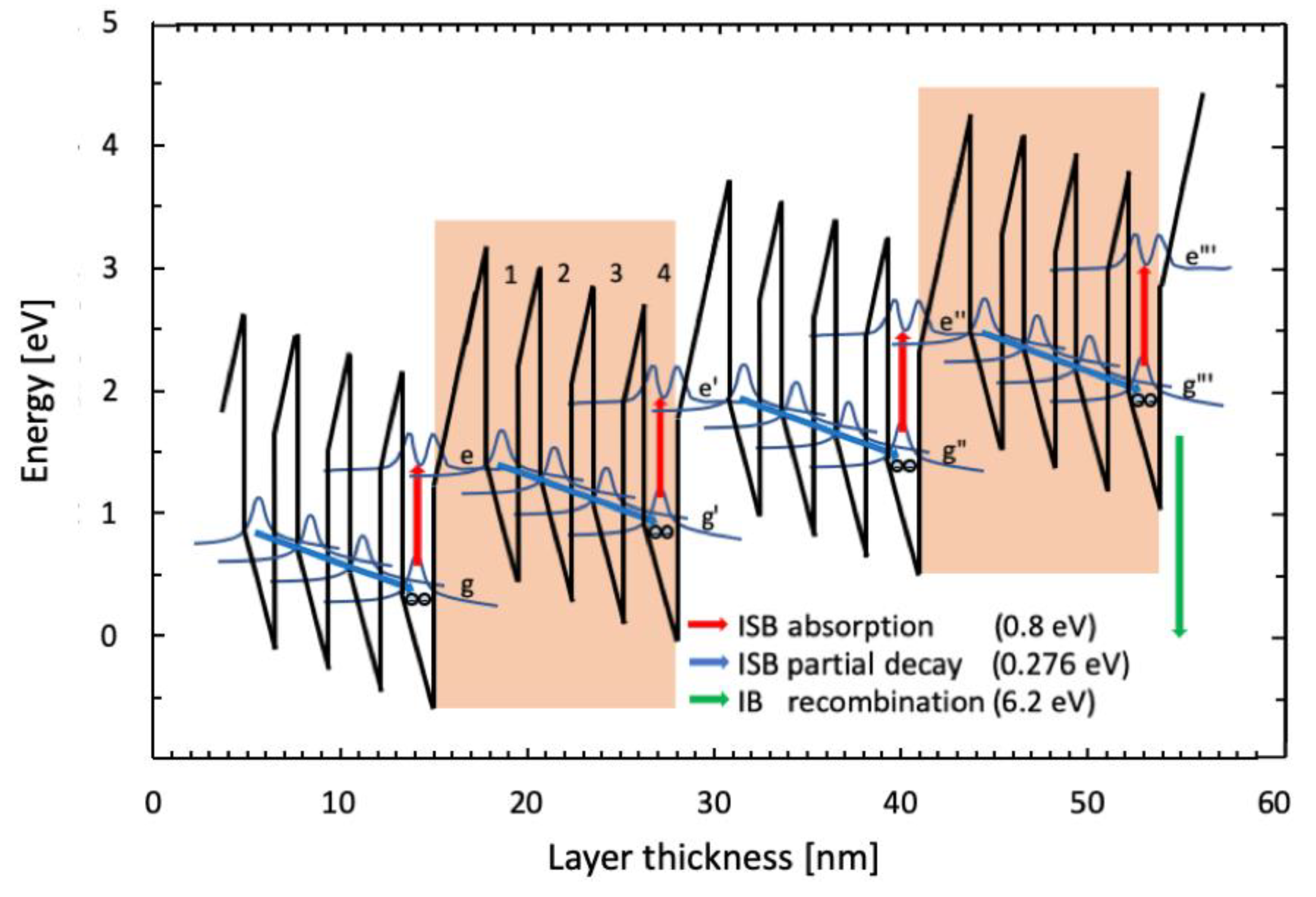
3. Proposed Operation of the Device

When applying zero bias voltage, the conduction band structure schematically appears sawtooth-shaped. There, the label ‘g’ denotes the first main well’s ground state while ‘e’ is its first excited state. Labels with primes (such as g’, g’’, …) indicate levels in the second, third, … main QW. In order to operate this device, a total voltage of 6.2 V (corresponding to an electric field of 413 kV/cm) will be applied between the top and the bottom contact layers of the mesa. This results in a stair-like conduction band structure; as shown in Figure 3. The above voltage will be carefully adjusted in order to result in a sufficiently small forward current (<1 mA)—indicating a slightly incomplete level alignment and a missing anti-crossing of the relevant energy levels ‘e’ and ‘1′ (see Figure 3). In order to provide the small amount of remaining electric field, the mesa under investigation will be illuminated vertically from above using light with a wavelength of 1.55 µm. The second-order grating diffracts this vertically incoming radiation into the directions parallel to the mesa surface. Due to subsequent light propagation in the horizontal direction, strong inter-subband absorption will take place in the 1.5 nm wide, n-doped GaN ([Si], ND = 2 × 1018 cm−3) QW layers.
As shown schematically in Figure 3, the absorbed near-IR radiation efficiently lifts electrons from the ground level (labelled level ‘g’) into the excited QW state (labelled level ‘e’). From there, the electrons have two possibilities to proceed. They will either drop back vertically into level ‘g’ or transfer—in a second step—towards the neighboring QW (labelled level ‘1’). Due to the specifically designed multiple LO-phonon resonances of the quantum stair, this process is extremely efficient and assumed to have a higher probability than the vertical one back to level ‘g’.
Therefore, those electrons which perform the above two-step process with absorption in the main QW and LO-phonon-induced transfer into well ‘1’ are very likely to further transit through the adjacent ‘quantum stair’. In this case, they will finally end up at the ground level of the next active region period (g’), from where they will be excited again. This way, they travel through the entire structure and they gain a certain amount of energy for each traversed period. At this point, the probability of such a multiple excitation process will be estimated.
After each optical excitation of 800 meV, the electrons will lose some of their acquired energy by undergoing three subsequent relaxations. This energy loss corresponds to three GaN-based LO-phonon energies (3 × 92 meV = 276 meV), thus roughly one-third of the initial energy of 800 meV. Since these optical pumping and decaying processes take place simultaneously in each of the 12 active region periods, a successive climbing across the entire quantum stair — at least of a certain fraction of the entire electron population—will occur. Obviously, we note that 12 × (0.8 − 0.276) eV = 6.288 eV is just slightly above the AlN bandgap of 6.2 eV. As this climbing constitutes the exact opposite of the ‘normal’ quantum cascade current flow, we will—as a net effect—see a slight reduction in the injection current.
How are we going to prevent the electrons from making a ‘too early’ recombination—i.e., already after two or three instead of 12 periods? Simply by growing only one single p-doped layer: namely the final layer of the structure. Therefore, the electrons have to reach the last (thin) QW layer of the structure. From there, the 12th optical absorption lifts the electrons onto a sufficiently high level to undergo afterward the desired inter-band recombination in AlN.
Concerning the efficiency of such a device, the following reasoning applies: an optical input power of 1 W will first be diffracted and lead to an ideal diffraction efficiency of 50% (i.e., 500 mW). This amount of power will be available for inter-subband excitation and carrier transport. By further admitting that—by a specific design exploiting a LO-phonon resonance as presented in reference [23]—a ‘two-step excitation/transfer’ towards level ‘1’ is (due to its shorter lifetime of τe1 = 0.3 ps) about three times as probable as a vertical transition back to level ‘g’ with τeg = 0.8 ps [24], we estimate a power of 375 mW going towards the ‘forward direction’ while only 125 mW will go towards the ‘backward direction’. This situation is equivalent to the one of a quantum cascade detector: While both the (‘inefficient’) vertical and the (‘desired’) diagonal excitation will be designed to have roughly the same probability of 50%, the diagonally excited electrons will be rapidly transferred by LO-phonon-assisted tunneling into the next well of the quantum stair. The carriers then swiftly reach the ground state of the following period, where they will be excited again. After 12 such excitations, we therefore obtain 1 W × (0.375 W/1 W)12 = 7.7 µW reaching the p-contact layer of the structure. With a roughly 80% conversion efficiency towards the deep-UV wavelength range, we estimate that a total power of 6 µW of deep-UV radiation at a wavelength as short as 200 nm will be generated in such a device. This value needs to be compared for instance with an AlN LED at λ = 210 nm emitting 0.02 mW (Taniyasu et al. [25]), an AlGaN LED at λ = 231 nm emitting 3.5 mW (Knauer et al. [26]), or an AlGaN LED at λ = 304 nm emitting 40 mW (Khan et al. [27]). From this short list, it becomes clear that going to an even shorter wavelength results in a rapidly decreasing output power.
Finally, as is quite generally the case for light-emitting diodes, the output will at first follow the torus-shaped radiation pattern typically seen in AlN (mainly horizontal radiation). However, it will then be efficiently diffracted towards a roughly vertical direction by the diffraction grating already used for the optical input.

4. Prospective Results

In order to measure this power with a sufficiently high signal-to-noise ratio, the incoming infrared radiation will be chopped at a frequency of 10 kHz. Although this could be done mechanically by a rotating chopper wheel, it is more efficient to perform this task electrically by directly applying a pulsed input signal between the top and the bottom contacts of the mesa. Between two electrical pulses, the conduction band structure is thus unbiased. During the electrical pulses, however, it looks biased like in Figure 3. Therefore, this structure changes periodically between its flat and its stair-like configuration. The resulting small difference in the injection current can be detected best using a sensitive lock-in technique. The latter typically allows the measurement of 1 % of the mean measurement values. In this case, this would be on the order of 1% × 6 µW = 60 nW.
Given the previously calculated 6 µW of deep-UV power for a near-IR input power of 1 W, a linear efficiency curve can be assumed in a first approximation. Figure 4 therefore presents the deep-UV output intensity as a function of near-IR optical input power.
Although the achievable output power of the proposed device with 6 µW seems to be relatively modest, one sees easily that this up-conversion has the potential for more interesting power levels. In addition, despite the fact that with AlN-based p-n-junction devices output powers approaching the 1 mW range have been achieved at a wavelength of 230 nm, going to an even shorter wavelength range will be fundamentally difficult. It is clear, however, that many interesting applications crucially rely on the additionally available photon energy corresponding to a wavelength of 200 nm instead of 230 nm. In any case, the device proposed here constitutes a useful intermediate approach until p-n-junctions in AlN are up to the point. Already at a modest device performance, more than 6 µW of deep-UV optical output power can be generated. In addition, the presented up-conversion approach is particularly interesting due to the fact that very powerful λ = 1.55 µm pump lasers are easily available. Finally, the optical excitation and relaxation scheme shown here is relatively simple and straightforward to implement.

5. Conclusions

In the present publication, we have outlined, conceived, and analyzed a new type of optical up-conversion device for the generation of deep-UV radiation. The proposed III-nitride semiconductor structure is based on carefully designed inter-subband transitions in a regular, chirped AlN/GaN-based superlattice. Using this structure, it will be possible to up-convert near-IR radiation into the deep-UV wavelength range. Although such multi-stage up-conversion processes are in general limited in their efficiency, the generated output power will in this case take advantage of the specific design. It uses LO-phonon-induced, mainly diagonal transfer of the excited charge carriers toward the ground state of the next period, thereby prolonging their lifetime quite considerably. In addition, the generated output power will obviously profit from readily available, watt-level optical input intensities in this important telecom wavelength range. Finally, thanks to better crystal growth, fabrication, and processing techniques—along with a higher level of characterization technology—considerable improvements are to be expected in the very near future.

Author Contributions

Conceptualization, D.H. and H.B.; methodology, D.H.; software, D.H. and H.B.; validation, D.P.B. and D.H.; formal analysis, D.H.; writing—original draft preparation, D.H.; writing—review and editing, D.H., H.B. and D.P.B. All authors have read and agreed to the published version of the manuscript.

Funding

This research received no external funding.

Data Availability Statement

The original data can be obtained from the first author of this article.

Acknowledgments

The authors would like to thank all of the involved colleagues and institutions—in particular, Lutz Kirste from the Institute of Applied Solid State Physics of the German Fraunhofer Gesellschaft and Cynthia Aku-Leh from ISCIENCES LLC. in Ann Arbor, MI, USA for their precious contributions to this work. We also greatly acknowledge scientific advice from John E. Epler from Lumileds, Inc., San Jose, CA, USA.

Conflicts of Interest

The authors declare no conflict of interest.

References

  1. Ruhnke, N.; Müller, A.; Eppich, B.; Maiwald, M.; Sumpf, N.; Erbert, G.; Tränkle, G. Compact deep UV system at 222.5 nm based on frequency doubling of GaN laser diode emission. IEEE Photonics Technol. Lett. 2018, 30, 289–292. [Google Scholar] [CrossRef]
  2. Den Engelsen, D.; Fern, G.R.; Ireland, T.G.; Harris, P.G.; Hobson, P.R.; Lipman, A.; Dhillon, R.; Marsh, P.J.; Silver, J. Ultraviolet and blue cathodoluminescence from cubic Y2O3 and Y2O3:Eu3+ generated in a transmission electron microscope. J. Mater. Chem. C 2016, 4, 7026. [Google Scholar] [CrossRef] [Green Version]
  3. Song, S.B.; Yoon, S.; Kim, S.Y.; Yang, S.; Seo, S.-Y.; Cha, S.; Jeong, H.-W.; Watanabe, K.; Taniguchi, T.; Lee, G.-H.; et al. Deep-ultra-violet electroluminescence and photocurrent generation in graphene/hBN/graphene heterostructures. Nat. Commun. 2021, 12, 7134. [Google Scholar] [CrossRef]
  4. Milleville, C.C.; Chen, E.Y.; Lennon, K.R.; Cleveland, J.M.; Kumar, A.; Zhang, J.; Bork, J.A.; Tessier, A.; LeBeau, J.M.; Chase, D.B.; et al. Engineering efficient photon upconversion in semiconductor heterostructures. ACS Nano 2019, 13, 489–497. [Google Scholar] [CrossRef] [PubMed]
  5. Sun, T.; Chen, B.; Guo, Y.; Zhu, Q.; Zhao, J.; Li, Y.; Chen, X.; Wu, Y.; Gao, Y.; Jin, L.; et al. Ultralarge anti-Stokes lasing through tandem upconversion. Nat. Commun. 2022, 13, 1032. [Google Scholar] [CrossRef]
  6. Motmaen, A.; Rostami, A.; Matloub, S. Ultra-high efficiency integrated mid infrared to visible up-conversion system. Sci. Rep. 2020, 10, 9325. [Google Scholar] [CrossRef] [PubMed]
  7. Kumamoto, Y.; Fujita, K.; Smith, N.I.; Kawata, S. Deep-UV biological imaging by lanthanide ion molecular protection. Biomed. Opt. Express 2016, 7, 158–170. [Google Scholar] [CrossRef] [Green Version]
  8. Mahboub, M.; Huang, Z.; Tang, M.L. Efficient infrared to visible upconversion with subsolar irradiance. Nano Lett. 2016, 16, 7169–7175. [Google Scholar] [CrossRef]
  9. Kallepalli, D.L.N.; Alshehri, A.L.; Marquez, D.T.; Andrzejewski, L.; Scaiano, J.C.; Bhardwaj, R. Ultra-high density optical data storage in common transparent plastics. Nat. Sci. Rep. 2016, 6, 26163. [Google Scholar] [CrossRef]
  10. Nakamura, S.; Fasol, G. The Blue Laser Diode: GaN Based Light Emitters and Lasers; Springer: Berlin/Heidelberg, Germany, 1997. [Google Scholar]
  11. Akasaki, I.; Amano, H.; Nakamura, S. The Nobel Prize in Physics. 2014. Available online: https://www.nobelprize.org/prizes/physics/2014/press-release (accessed on 14 April 2015).
  12. Murayama, M.; Nakayama, Y.; Yamazaki, K.; Hoshina, Y.; Watanabe, H.; Fuutagawa, N.; Kawanishi, H.; Uemura, T.; Narui, H. Watt-class green (530 nm) and blue (465 nm) laser diodes. Phys. Status Solidi A 2018, 215, 1700513. [Google Scholar] [CrossRef]
  13. Hofstetter, D.; Baumann, E.; Giorgetta, F.R.; Théron, R.; Wu, H.; Schaff, W.J.; Dawlaty, J.; George, P.A.; Eastman, L.F.; Rana, F.; et al. Photodetector based on intersubband transitions using III-nitride superlattice structures. J. Phys. Condens. Matter 2009, 21, 174208. [Google Scholar] [CrossRef] [PubMed] [Green Version]
  14. Giorgetta, F.R.; Baumann, E.; Guillot, F.; Monroy, E.; Hofstetter, D. High frequency (f = 2.37 GHz) room temperature operation of 1.55 µm AlN/GaN intersubband detector. Electron. Lett. 2007, 43, 185–187. [Google Scholar] [CrossRef]
  15. Shur, M.S.; Gaska, R. Deep-ultraviolet light-emitting diodes. IEEE Trans. Electron Devices 2010, 57, 12–25. [Google Scholar] [CrossRef]
  16. Song, K.; Mohseni, M.; Taghipour, F. Application of ultraviolet light-emitting diodes (UV-LEDs) for water disinfection: A review. Water Res. 2016, 94, 341–349. [Google Scholar] [CrossRef] [PubMed]
  17. SaifAddin, B.K.; Almogbel, A.S.; Zollner, C.J.; Wu, F.; Bonef, B.; Iza, M.; Nakamura, S.; Speck, J.S. AlGaN deep-ultraviolet light-emitting diodes grown on SiC substrates. ACS Photonics 2020, 7, 554–561. [Google Scholar] [CrossRef]
  18. Ichimura, I.; Maeda, F.; Osato, K.; Yamamoto, K.; Kasami, Y. Optical disk recording using a GaN blue-violet laser diode. Jpn. J. Appl. Phys. 2000, 39, 937. [Google Scholar] [CrossRef]
  19. Wang, D.; Uesugi, K.; Xiao, S.; Norimatsu, K.; Miyake, H. High-quality AlN/sapphire templates prepared by thermal cycle annealing for high-performance ultraviolet light-emitting. Appl. Phys. Express 2021, 14, 035505. [Google Scholar] [CrossRef]
  20. Ahmad, H.; Lindemuth, J.; Engel, Z.; Matthews, C.M.; McCrone, T.M.; Doolittle, W.A. Substantial p-type conductivity of AlN achieved via Beryllium doping. Adv. Mater. 2021, 33, 2104497. [Google Scholar] [CrossRef]
  21. Shul, R.J.; McClellan, G.B.; Casalnuovo, S.A.; Rieger, D.J.; Pearton, S.J.; Constantine, C.; Barratt, C.; Karlicek, R.F., Jr.; Tran, C.; Schurman, M. Inductively coupled plasma etching of GaN. Appl. Phys. Lett. 1996, 69, 1119–1121. [Google Scholar] [CrossRef]
  22. Evans, G.A.; Butler, J.K.; He, R.-H.; Kirk, J.B.; Yao, J.; Zheng, X.; Krishnamoorthy, A.V. Enhanced coupling strength gratings for couplers in III-V-compound dielectric waveguides. IEEE J. Light. Technol. 2017, 35, 2234–2242. [Google Scholar] [CrossRef]
  23. Graf, M.; Scalari, G.; Hofstetter, D.; Faist, J.; Beere, H.; Linfield, E.; Ritchie, D.; Davies, G. Terahertz range quantum-well infrared photodetector. Appl. Phys. Lett. 2004, 84, 475–477. [Google Scholar] [CrossRef]
  24. Heber, J.D.; Gmachl, C.; Ng, N.M.; Cho, A.Y. Comparative study of ultrafast intersubband electron scattering times at ~1.55 µm wavelength in GaN/AlGaN heterostructures. Appl. Phys. Lett. 2002, 81, 1237–1239. [Google Scholar] [CrossRef]
  25. Taniyasu, Y.; Kasu, M.; Makimoto, T. An aluminium nitride light-emitting diode with a wavelength of 210 nanometres. Nature 2006, 441, 325–328. [Google Scholar] [CrossRef] [PubMed]
  26. Knauer, A.; Kolbe, T.; Hagedorn, S.; Hoepfner, J.; Guttmann, M.; Cho, H.K.; Rass, J.; Ruschel, J.; Einfeldt, S.; Kneissl, M.; et al. Strain induced power enhancement of far-UVC LEDs on high temperature annelaed AlN templates. Appl. Phys. Lett. 2023, 122, 011102. [Google Scholar] [CrossRef]
  27. Khan, M.A.; Noritoshi, M.; Joosun, Y.; Masafumi, J.; Yoichi, Y.; Hirayama, H. Achieving 9.6% efficiency in 304 nm p-AlGaN UVB LED via increasing the holes injection and light reflectance. Sci. Rep. 2022, 12, 2591. [Google Scholar] [CrossRef] [PubMed]
Figure 1. Scanning electron microscopy (SEM) image of a second-order diffraction grating for vertical coupling. The period of this grating is Λ = 674 nm, as shown by the scale bar. The metal layers are identical to the p-type metallization used for the contacts.
Crystals 13 00494 g001
Figure 2. Schematic drawing of the square-shaped AlN/GaN-based inter-subband mesa with a diffraction grating on top. Metallization allows electrical contact at the top and the bottom of the mesa.
Crystals 13 00494 g002
Figure 3. Conduction band structure under an applied bias voltage of 6.2 V on 12 periods—corresponding to an electric field of 413 kV/cm. QWs/barriers 1, 2, 3, 4 correspond to one SL period. Excitation through photon absorption (vertical red arrows) and partial relaxation (oblique blue arrows) are schematically shown. The vertical transition energy in the main QW measures 800 meV (λ = 1.55 µm). The green arrow marks the interband transition in the deep-UV.
Crystals 13 00494 g003
Figure 4. Calculated output intensity at an energy corresponding to the AlN bandgap of 6.2 eV (λ = 200 nm) as a function of optical illumination at λ = 1.55 µm. For the available range of input intensities, no pronounced saturation effects are to be expected.
Crystals 13 00494 g004
Disclaimer/Publisher’s Note: The statements, opinions and data contained in all publications are solely those of the individual author(s) and contributor(s) and not of MDPI and/or the editor(s). MDPI and/or the editor(s) disclaim responsibility for any injury to people or property resulting from any ideas, methods, instructions or products referred to in the content.

