1. Introduction
III-N wide bandgap semiconductors such as GaN and its alloys with indium or aluminum are widely used for manufacturing LEDs, laser diodes, photovoltaics, and high-frequency high-power devices [
1,
2,
3]. GaN has the potential for high pressure, high temperature, and high voltage applications due to its high critical electric field, good thermal conductivity, and high electron mobility [
4,
5].
Today, most white LED lamps are based on down conversion when phosphors absorb light from UV or blue LEDs and then re-emit photons at lower energies resulting in a white spectrum. However, the energy losses using down conversion can be about 20–30% depending on the wavelength due to the Stokes shift [
6]. These losses can be avoided if a multi-chip design with red, green, and blue LEDs is used with color-mixing optics. Currently, there are red LEDs based on alloys of GaAsP and blue LEDs based on InGaN with relatively low In content demonstrating high quantum efficiencies exceeding 80% [
7]. However, efficient green LEDs emitting around 550–600 nm are still difficult to manufacture. This phenomenon is known as the green gap [
8]. The origin of the green gap is related to the degradation in crystalline quality and piezoelectric fields in strained InGaN quantum wells (QWs) due to an increase in lattice mismatch between In
1−xGa
xN and the underlying GaN, which is roughly 1% for every 0.1 indium mole fraction “
x” [
9,
10]. This gives rise to the poor structural quality of the material, especially for thicker layers and it will result in reduced efficiency of the InGaN-based LEDs. The problem is further complicated when growth is performed on foreign substrates such as on the commonly used sapphire (Al
2O
3) or silicon carbide (SiC) that have a significant lattice mismatch with GaN of ~16 and 3%, respectively [
11,
12]. The lattice mismatch results in an increased density of threading dislocations that act as non-radiative recombination channels, which is a critical issue in the In-rich InGaN-based LEDs [
13]. To reduce stress, it is advantageous to fabricate thick lattice-matched InGaN layers of high crystalline quality that can be used as initial templates for further growth of InGaN-based device structures.
To overcome the abovementioned problems several different techniques to fabricate LEDs by growth on a relaxed InGaN layer have been suggested [
14]. For example, highly relaxed thick layers of InGaN templates [
15], growth on thermally decomposed InGaN layers [
16], growth of InGaN on lattice-matched ScAlMgO
4 substrates [
17,
18], growth of relaxed InGaN on InGaN pseudo-substrates [
19,
20], and relaxed InGaN templates grown on porous GaN [
21].
Molecular beam epitaxy (MBE) and metal-organic vapor phase epitaxy (MOVPE) are common methods for fabricating epitaxial layers and heterostructures for various III-N applications. However, due to low growth rates (<1 µm/h) these methods are not suitable for growing thick III-N layers that can be used as templates. Another problem is related to the tendency of In
1−xGa
xN to phase-segregate into In-rich and Ga-rich alloy regions during the growth, especially as the indium fraction increases [
22]. This is partly caused by a high surface mobility of the In atoms compared to the Ga atoms and the large disparity in the vapor pressures of these two metals. While halide vapor phase epitaxy (HVPE) is a more promising technique to produce thick GaN layers at ~1000 °C due to high growth rates in the range of 10–100 µm/h [
23,
24], it remains challenging to reduce the growth temperature to ~500–600 °C, i.e., to temperatures necessary to prevent thermal segregation of InGaN. This is because the cracking efficiency of ammonia, which is a typical precursor of nitrogen, sharply reduces at temperatures below 1000 °C, which results in low growth rates and poor crystal quality [
25].
Thus, in this work, we report the development of a proof-of-concept method to grow GaN layers using a plasma-assisted HVPE (PA-HVPE) process. The implementation of the plasma source in the reactor chamber before the sample holder allows ammonia to be activated even at lower growth temperatures of ~570 °C, which results in an increase in growth rates by a factor of 2 up to 5 µm/h. We have also used metallic indium to form in situ precursors of InCl/InCl3 with the aim of studying the possibility of In incorporation during HVPE growth.
2. Materials and Methods
For the experiments, we used a horizontal homemade HVPE reactor schematically shown in
Figure 1. The HVPE system consists of a resistively heated oven with three zones. Each temperature zone can be controlled and heated up to 1050 °C. The system has two boats for in situ generation of GaCl and InCl
3/InCl by flowing HCl over metal melts. The Ga and In metals have a purity of 7 N. Nitrogen was used as carrier gas and the pressure in the reactor during growth was 500 mbar. The HCl flow over the Ga melt was kept constant at 5 mL/min, and, for the In melt, the flow was varied in the range of 2–10 mL/min. The NH
3 and N
2 gas flows were kept constant at 80 mL/min and 1000 mL/min, respectively. The temperature of the metal melts can be varied by changing the position of the boats in the reactor. In this study, the temperature of the Ga melt was 700 °C, while the temperature of the In melt was varied in the range of 260 to 460 °C. As a substrate for the growth, both
c-axis Al
2O
3 with a thickness of 450 µm and GaN templates were used. The GaN templates were commercially available templates consisting of a 3 µm thick MOVPE GaN layer grown on
c-axis Al
2O
3 wafers with a thickness of 430 µm. Since the growth of high-quality GaN on foreign substrates, such as sapphire, requires several elaborate steps to form a nucleation layer [
26], we have mainly carried out homoepitaxial growth on GaN templates in this work. The size of the samples was 1 cm × 1 cm.
For plasma generation, dielectric barrier discharge (DBD) was used, where the plasma was generated between two graphite electrodes with a 430 µm thick Al
2O
3 wafer acting as a dielectric (
Figure 2a). The gap distance d was 5 mm. The electronics for the plasma generation control consists of four 15 kV high-voltage switches connected in a so-called H-bridge, in which the polarity between the electrodes can be changed by alternately turning on and off each pair of switches (S1, S4) and (S2, S3). Two 15 kV MOSFET push-pull high-voltage switches (BEHLKE HTS 151-03-GSM) and a high-voltage unit (Heinzinger EVO10000-200rev) were used. Plasma generation was carried out using a voltage of ~3–5 kV. The pulse width was limited to 10 µs since longer pulses resulted in discharging and an unstable plasma. The pulse repetition frequency was limited to 5 kHz by the MOSFET push-pull high-voltage switches.
Figure 2b schematically shows a typical pulse sequence with “on” and “off” times. The HVPE growth of GaN is commonly performed at atmospheric pressure. At such pressures, it was difficult to obtain a stable nitrogen plasma even at high temperatures. Therefore, the growth of the studied layers was done at a lower pressure of 500 mbar. To prevent arc-discharge due to parasitic deposition on the electrodes, the growth time was limited to 15 min.
The thickness of the layers was estimated from the weight of the samples before and after growth to give quick feedback to the growth runs, but it was also confirmed by measurements using scanning electron microscopy (SEM) and white light reflectance spectroscopy (WLRS).
Optical characterization was performed by cathodoluminescence (CL) measurements at different temperatures from ~5 to 295 K using a MonoCL4 setup in situ SEM instrument LEO1550. For plasma and transmission spectra measurements, we used a Thorlabs fiber-based compact Czerny-Turner CCD spectrometer, model CCS200/M. Atomic force microscopy (AFM) measurements were performed using a Dimension 3100 SPM microscope with the VT-102 vibration isolation table. X-ray diffraction (XRD) measurements were done using a PANalytical X’Pert Pro diffractometer with Cu-Kα radiation.
3. Results and Discussion
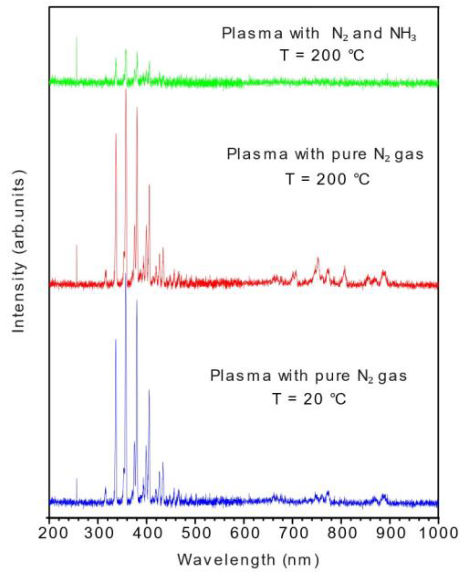
Figure 3 shows optical spectra of the nitrogen plasma generated between the electrodes inside the reactor with parameters used during the growth of samples. Measurements are shown for 20 and 200 °C for pure nitrogen (blue and red lines) and when ammonia with a flow of 80 mL/min was added in the chamber (green lines). At higher temperatures, the chamber was protected by an isolating shield, which prevented optical measurements. The plasma spectrum shows peaks in the range of 300–500 nm related to the transitions of the N
2 s positive system (2PS) overlapping with N
2+ first negative system (1NS) originating from the transition between the excited states and the ground state of molecular ion N
2+ [
27]. Electronic transitions in the region of 500–900 nm are related to the first positive system (1PS) of N
2 [
28]. The 1PS lines become more intense at 200 °C. We also observed at this temperature a weak sharp line at ~746.6 nm, which might correspond to the excited nitrogen atom transition at 746.83 nm.
When the ammonia gas was added, the intensities of the transition peaks decrease as can be seen in
Figure 3 for the plasma spectrum shown by the green line. In this case, the spectrum was dominated mainly by the 2PS transitions, while no additional lines were observed, although the transition at 746.6 nm was still present in the spectrum. We also observed a sharp peak at ~256.6 nm in all measured plasma spectra. The origin of this peak has not yet been identified; however, it is not related to the response function of the instrument, but to some unknown species in the plasma.
First, the HVPE growth of GaN layers at a low temperature of ~600 °C was performed without and with plasma generation. The thickness of the layers increased from 0.17 µm to 0.5 µm, which means a significant increase in the growth rate from ~0.6 µm/h to 2 µm/h by activation of ammonia using the plasma source. The deposition in this particular case was done directly on a sapphire substrate to avoid any influence on the layer properties from the MOVPE GaN templates. When growth is performed on sapphire, the growth rate is not constant and is lower before coalescence.
Using the GaN templates, the growth rate at ~600 °C increases to ~4–5 µm/h for the samples produced with ammonia activated by plasma, while attempts to grow GaN layers without plasma generation resulted in much lower growth rates of ~1.2 µm/h.
SEM measurements confirmed that the estimation of thickness from the weight gives a reasonable average value. For the sample in
Figure 4a, the HVPE layer thickness determined from the weight measurements was 0.96 µm, and from the SEM image was 0.95 µm.
Figure 4b shows a thickness map of a layer grown at 620 °C on a GaN template. For this layer, the average thickness of ~1.6 µm was determined from the weight measurements, which correlates with the thickness map, where the variation in thickness was obtained in the range of 1.3–1.7 µm. There is a gradient in the thickness over the sample (~25%) in the direction of the gas flow. Thus, for scaling up the process and deposition of larger areas, the system requires rotation of the sample and/or higher carrier gas flows. The roughness is ~14 nm for the root mean square (RMS) as estimated from AFM measurements in
Figure 4c.
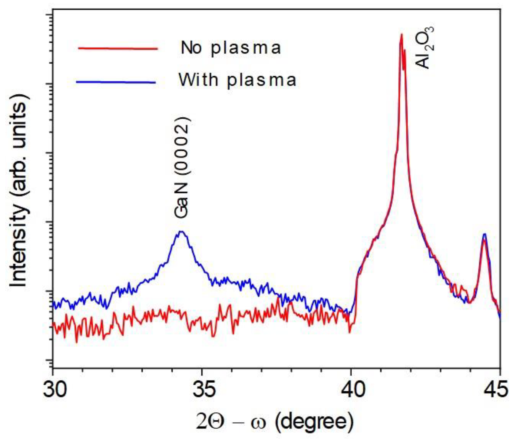
The structural quality of the GaN layers grown directly on sapphire was examined by XRD (see
Figure 5). The GaN layer grown with plasma generation shows a reflection peak from the (0002) plane and, thus, an alignment to the c-axis, while the sample grown without ammonia activation shows only a sapphire-related peak.
We have investigated the possibility of indium incorporation in GaN using the PA-HVPE process with different temperatures of the boat with metallic indium, with different HCl flows over the boat with indium. The process was also studied using growth temperatures of 570 and 620 °C. The XRD patterns measured for the symmetric (0002) reflection are shown in
Figure 6a for samples grown at 620 °C at three different temperatures of the metallic indium. The dominating diffraction peak is related to GaN, which also involves a reflection from the GaN template. Therefore, to distinguish signals from the HVPE layers and the MOVPE GaN template, grazing incidence XRD (GIXRD) 2θ scans with an incident angle of 0.5 degrees were acquired (
Figure 6b). Clearly, for the samples grown at different temperatures of the metallic indium, the XRD peak position shifts towards lower angles, which indicates the incorporation of indium in GaN. Note that the thickness of all layers was ~1 µm, which means that the layers can be considered to be fully relaxed [
25]. In this case, the lattice constant
c can be determined from the X-ray (0002) peak position according to the Bragg law and the indium molar fraction x can be calculated from Vegard’s law:
To estimate the indium concentration in the layers from XRD data, we have used values of 5.702 and 5.185 Å for the lattice parameter
c of InN and GaN, respectively [
29]. The obtained x values are plotted in the inset of
Figure 6b for different growth parameters. The highest indium concentration of ~8% was obtained for the medium boat temperature of ~320 °C and HCl flow of 10 mL/min. However, the XRD method to assess indium composition in InGaN depends on the lattice parameters, which have a spread of values according to the literature [
29], which can arise to inaccuracies. The rocking curves are rather broad with full widths at half maximum (FWHM) of ~0.1 and ~0.16 degrees for (0002) GaN and InGaN reflections, respectively (see
Figure 6c), which indicates structural imperfections. This is an additional problem contributing to the determination of lattice parameters and, thus, to correctly estimating In content from XRD measurements. Nevertheless, GIXRD has been shown as a feasible technique to study InGaN films with various In% on Si substrate [
30].
Furthermore, SIMS analysis shows that, although indium indeed incorporates in the HVPE layers at 620 °C, the estimated concentration was lower than that obtained from XRD data. The depth profiles of indium content for samples grown at 620 °C with HCl flows of 5 and 10 mL/min and with the ammonia activated by plasma are shown in
Figure 7a in the linear scale. For comparison, the indium concentration profile is also plotted for the layer grown with the same parameters but without plasma generation in
Figure 7b. Clearly, the growth rate is twice as high with plasma-assisted growth. The activated ammonia concentration is higher after the plasma source and that gives rise to a higher growth rate of GaN. At the same time, plasma has a negative effect on indium concentration because plasma simultaneously activates chlorine-containing species. The relatively poor bonding ability of In compared to Ga in InGaN means that In can be more easily etched by the highly reactive plasma-activated chlorine-containing species and that will result in a lower In concentration [
31,
32]. In addition, it is also known that the growth of InGaN does not occur when InCl is used since the equilibrium constant of the reaction between InCl and NH
3 is small [
33]. Since the InCl
3 in our system is passed through the plasma, we cannot rule out that some of the In precursors are decomposed to InCl. Thus, to improve the incorporation of In in the layers, the precursors InCl
3 and GaCl should bypass the plasma.
The band gap shift caused by different concentrations of indium in the InGaN layers grown using plasma-activated ammonia can be observed in transmission measurements. Then, the optical band gap can be estimated from the absorption coefficient α. For the direct band gap semiconductors α is related to the band gap energy
Eg as follows:
where
E is the photon energy. Graphs of
α2E2 as a function of photon energy in the vicinity of the band edge are shown in
Figure 8a for samples grown with different HCl flows through the boat with indium. The reference spectrum for the GaN template is also shown in the inset. The shift in the absorption edge is clearly seen in
Figure 8b for the samples grown using different temperatures of the indium melt. The energy of the band gap can be estimated by extrapolating the linear part of
α2E2 to zero as indicated in
Figure 8a by dashed lines. The extracted values of
Eg are plotted in
Figure 9a,b for the same samples as in
Figure 8. Note, the optical band energy of 3.396 eV estimated for the GaN template is slightly higher than the 3.39 eV for relaxed GaN, which is common for layers under compression when grown on sapphire [
34].
The energy of the bandgap for alloy In
xGa
1 − xN can be approximated by Vegard’s law:
which allows the calculation of the indium composition x. Using the bandgap energy of 3.39 and 0.7 eV for GaN and InN [
25], respectively, and the InGaN bandgap energy from the absorption data, we have determined that the indium concentration does not exceed 3% in the layers grown with plasma-activated ammonia. Taking into account nonlinearity in the InGaN band gap with bowing parameter in the range between ~1.3 and 3.8 eV [
35,
36], the indium concentration can be lower. This result correlates well with the data obtained by the SIMS analysis. Indium concentrations determined by different techniques are collected in
Table 1. The discrepancy in the determination of indium content has several causes. First, the estimation of indium fraction by SIMS can give an error due to the matrix effect as SIMS is mainly used for the determination of the concentrations of impurities [
37]. Second, the extraction of lattice constant
c from the XRD patterns can be also inaccurate due to broad XRD peaks and material imperfection. Thus, there is a moderate overestimation in In content determined by GIXRD compared to absorption spectra. Similar observations have also been reported when comparing In% determined by various techniques [
30].
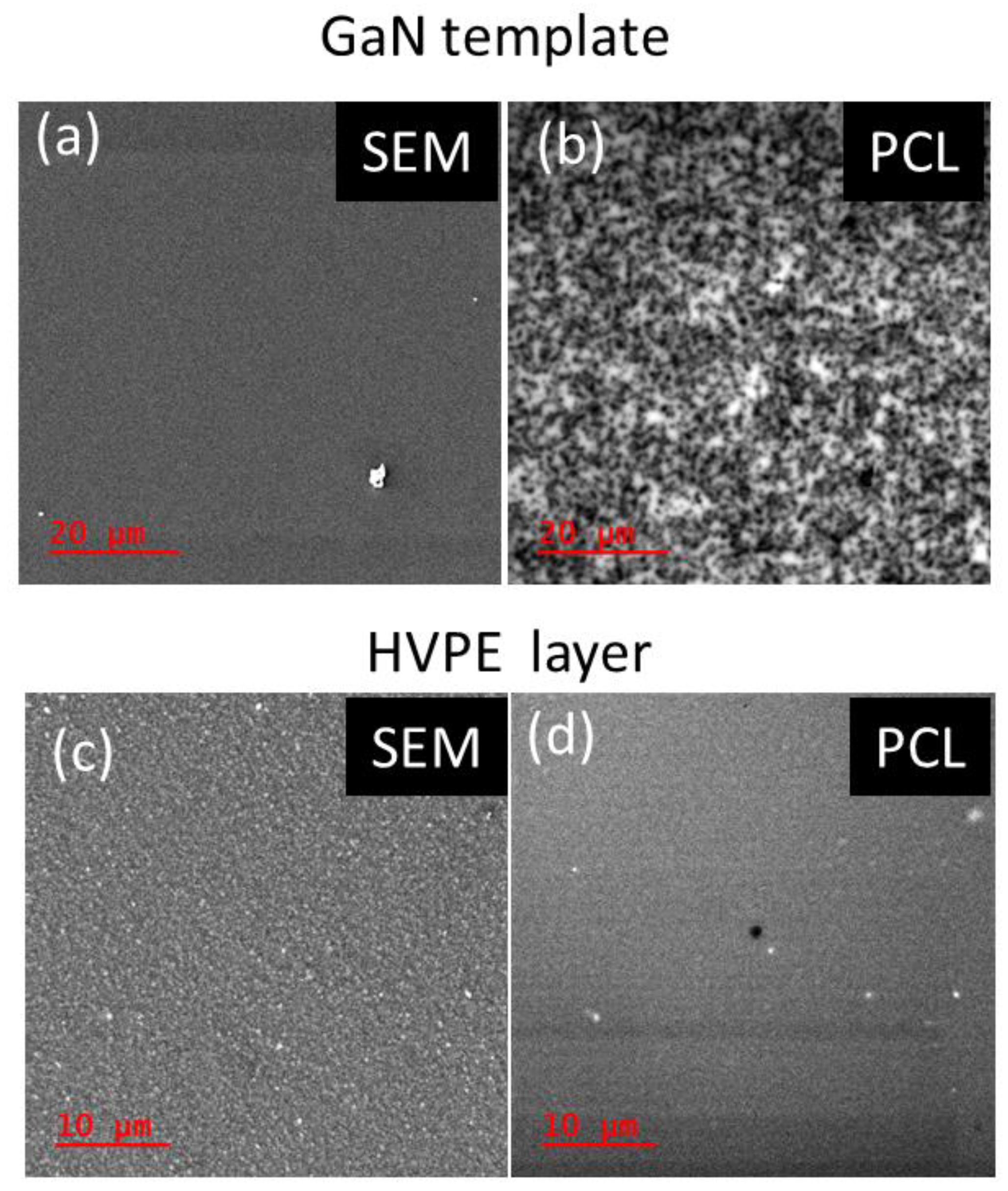
The emission properties have been studied by low-temperature CL simultaneously with SEM measurements. The morphology of the studied layers produced with plasma generation shows a rougher surface compared to the MOVPE GaN layer (template) (see
Figure 10a,c). At the same time, panchromatic CL (PCL) images at 5 K demonstrate that threading dislocations observed as dark spots in the image for the GaN template (
Figure 10b) are likely overgrown during the HVPE process judging from the PCL image, which demonstrates uniform contrast (
Figure 10d). A similar tendency to overgrow threading dislocations has been observed previously in HVPE GaN layers [
38]. However, the uniform contrast in
Figure 10d can be also caused by the presence of strong nonradiative centers over the entire InGaN layer, which will prevent the decoration of threading dislocations.
Examples of CL spectra measured at 5 K for the samples grown with three different process parameters are shown in
Figure 11. The reference CL spectrum for the GaN template is shown by the dashed line. CL spectra for all studied samples grown by using plasma-activated ammonia are dominated by defect luminescence. Increasing the HCl flow over the indium melt at a boat temperature of 320 °C results in the shift of the maximum of the defect luminescence to the lower photon energies for the samples grown at 570 °C (
Figure 11a). The influence of the indium boat temperature on the luminescence is also noticeable as shown for the layer grown at 620 °C with a constant HCl flow of 5 mL/min (
Figure 11b). CL spectra measured at different temperature for the layer grown with a constant HCl flow of 10 mL/min through the indium boat is presented in
Figure 11c. The ratio of the integrated intensities for the defect emission at 5 K and room temperature is ~2.5. The layer shows rather uniform emission properties with the same peak position independently of the point of acquisition as shown in
Figure 11d. Conversely, for different samples, the shift of the CL band maximum correlates with the increased concentration of indium precursor and with indium content determined by XRD. Similar luminescence was observed for plasma-assisted MBE InGaN samples, where the emission shift was assigned to the increasing indium content [
39]. In our case, however, the observed CL shift can hardly be attributed to the narrowing of the band gap of In
xGa
1−xN with increasing x, as the variation of the optical band gap does not exceed 30 meV, while the shift of the CL bands is more than 300 meV and ranged between 2.2 eV and 1.85 eV. The observed emissions will be, thus, considered as related to defect luminescence in GaN, known as yellow (YL) and red (RL) bands. Similar RL has been observed in HVPE GaN samples but it is not so common for MOVPE GaN [
40]. Although the position of the RL bands is around 1.8 eV, it can be caused by different defects with different properties, and the nature of the RL band is yet to be revealed. The YL1 band with the maximum at 2.2 eV is better studied and associated recently with a carbon-related defect (C
N) rather than defects involving Ga vacancy [
40]. YL1 is typical for MOVPE GaN layers where metal-organics are used as Ga precursor. In HVPE samples, the carbon concentration is usually very low. While YL1 is not pronounced in the undoped HVPE GaN, it appears under doping with carbon impurity [
41]. Here, using graphite plasma electrodes for ammonia activation, carbon species can be produced, which explains the strong YL1 emission. The observed shift in the emission to red wavelengths and the enhancement in the RL band are correlated with an increased concentration of indium precursor (i.e., InCl or InCl
3). Considering that RL is typical for HVPE-grown GaN, our observation may indicate that the origin of the RL band is related to the chlorine-containing impurities.


