Article

Ultrathin Rare-Earth-Doped MoS2 Crystalline Films Prepared with Magnetron Sputtering and Ar + H2 Post-Annealing

1
School of Physics, Beijing Institute of Technology, Beijing 100081, China
2
Key Lab for Advanced Materials Processing Technology of Ministry of Education, School of Materials Science and Engineering, Tsinghua University, Beijing 100084, China
3
Physics Department, University of Oslo, N-0316 Oslo, Norway
*
Author to whom correspondence should be addressed.
Crystals 2023, 13(2), 308; https://doi.org/10.3390/cryst13020308
Submission received: 12 January 2023 / Revised: 2 February 2023 / Accepted: 8 February 2023 / Published: 13 February 2023
(This article belongs to the Special Issue Rare Earths-Doped Materials (Volume II))

Abstract

:
In this work, we propose a method to prepare large-area, crystalline ultrathin rare-earth (RE, i.e., Eu, Yb, Er and Tb)-doped MoS2 thin films, using magnetron sputtering and subsequent Ar + H2 annealing. The film thickness of as-deposited samples varied from 60 to 100 nm, and decreases to be below 10 nm after annealing at 550 °C for 30 min. X-ray diffraction and Raman spectra analysis revealed that the sample films were crystallized after the annealing, which resulted in a MoS2 crystallite size of about 4–5 nm. X-ray photoelectron spectroscopy indicated that most of the RE ions existed in the films in trivalent states. The optical bandgap of the RE-doped MoS2 samples decreased from 1.6 eV (undoped) to 1.3 eV (Eu-doped) in the UV-vis absorption spectra. Electrical measurements showed that the electrical resistance decreased from 9.13 MΩ (undoped) to 0.34 MΩ (Yb-doped), the carrier density increased by one to two orders of magnitude and the carrier mobility decreased from 5.4 cm2/V·s (undoped) to 0.65 cm2/V·s (Yb-doped). The sign of the Hall coefficients indicated that the undoped MoS2 and the Yb-, Tb- and Er-doped MoS2 samples were n-type semiconductors, while the Eu-doped sample showed p-type characteristics. This study may be helpful to broaden the photoelectronic applications of these two-dimensional materials.

1. Introduction

In recent years, two-dimensional (2D) materials have attracted enormous interest for their potential applications in optoelectronic and nanoelectronic devices [1,2,3,4,5,6]. Compared to the zero-energy bandgaps of graphene materials, transition metal dichalcogenides (TMDs) such as molybdenum disulfide (MoS2) have considerable bandgaps, varying from 1.2 eV (bulk) to 1.8 eV (monolayer) [7]. Atomically thin (i.e., monolayer and few-layer) MoS2 variants have unique electronic structure and are recognized as potential materials for the next generation of photoelectronic devices. For example, monolayers of MoS2 have displayed large current on/off ratios (>108), high effective mobility of up to 1000 cm2/(V·s) and high photoresponsivity (880 A/W @532 nm irradiation) [8,9,10], while few-layer MoS2 examples have adjustable bandgaps with large exciton-binding energies and surface charge density, making them widely used in fabricating field-effect transistor-based gas sensors, photodetectors, photocatalyst devices and so on [11,12,13,14,15].
Doping is an effective method to modify the photonic properties of MoS2. Rare-earth (RE) ions have unique 4f electronic transitions, including the f-d interconfigurational and f-f intraconfigurational transitions. Doping of MoS2 with RE ions may enhance absorption and emission of near-IR photons [16,17], in which the energy transfer between the host and the RE ions can be mediated through intrinsic defect states within the MoS2. For example, down-conversion (DC) in the NIR region and up-conversion (UC) in the visible red region were realized in an Er3+-doped MoS2 system [18]. Sm-doping of MoS2 has significantly improved the electrical performance of monolayer MoS2-based field effect transistors [19] and demonstrated to be an effective material for improving photocatalytic hydrogen evolution with the assistance of Co [20]. In addition, CeO2-MoS2 nanocomposites have enhanced visible-light photocatalytic activity compared to those of bare MoS2 and CeO2 [21].
Various techniques and technologies have been adopted to fabricate monolayer/few-layer MoS2 or ultrathin MoS2 films, such as mechanical exfoliation [22], liquid exfoliation [23], the electrochemical lithiation process [24], chemical vapor deposition (CVD) [25], physical vapor deposition (PVD), atomic layer deposition (ALD) [26] and so on. Among them, methods of mechanical exfoliation and CVD are suitable to produce high-quality single- or few-layer MoS2 films but have the drawbacks of poor yields and difficulty in scale-up. Methods of PVD such as thermal evaporation [27] and pulsed laser deposition [16] have also been reported as reliable methods for single/few-MoS2-layer deposition, with potential to scale up to full wafer size. In particular, magnetron sputtering techniques were adopted to fabricate single/few-layer MoS2 films with or without RE doping [28,29,30,31]. The crystalline structure and properties of sputter-grown MoS2 films strongly depend on the deposition conditions, such as substrate temperature, working gas pressure and substrate materials [28]. For example, as-grown semiconducting (002) textured 2H-MoS2 could take the form of nanocrystalline (3–10 nm grain size) films at substrate temperatures higher than 350 °C or amorphous films when deposited at room temperature [11]. Through analyzing successful deposition of MoS2 thin films, one can believe that the main obstacle for large-area, sputtered and high-quality MoS2 films is possibly the difficulty of disorder control during film deposition, and this could hopefully be controlled through optimizing process parameters [29]. Among these, substrate temperature during RF sputtering of MoS2 has been reported to yield significantly improved crystallinity of MoS2 films when increased from 250 °C [28] up to 400 °C [30]. Postdeposition annealing of room-temperature-grown films in vacuum [29], N2 [31] or argon [32], or using a high-power pulsed laser [11], is an alternative choice to improve the crystallinity of MoS2 thin films.
Therefore, in this work, we deposited ultrathin MoS2 and RE-doped MoS2 films using magnetron sputtering and improved the crystallinity of these films using post-deposition annealing in Ar + 10% H2. The structural, optical and electrical properties of these films were investigated with respect to various RE doping. The present results indicate that this fabrication technology can be promisingly used to fabricate higher-quality MoS2 films for application in a wide variety of electronic and optoelectronic devices.

2. Experimental Details

The ultrathin MoS2 films and RE-doped MoS2 films were deposited on SiO2 (300 nm)/Si or sapphire substrates via magnetron-sputtering different composite targets for different RE dopants. Before sputtering, the substrates were ultrasonically cleaned sequentially in acetone, ethanol and deionized water. The base vacuum pressure was about 2.3 × 10⁻⁴ Pa and the vacuum chamber was heated to 100 °C before the deposition. During the sputtering, the working gas ambience was argon with a flow rate of 25.0 sccm, and the gas pressure was about 1.0 Pa. For the deposition of MoS2 films, the composite target was a pure MoS2 target with a purity of 99.99% and two small sulphur (S) platelets (purity: 99.9999%; about Φ3 mm × 1 mm) placed on the surface of the MoS2 target to make up for the loss of S during the sputtering. For the deposition of erbium (Er)-doped MoS2 (MoS2 + Er) films, small, metal Er platelets (purity: 99.99%) were placed on the MoS2 target together with the two S platelets. For the deposition of europium (Eu)-doped MoS2 (MoS2 + Eu) films, an EuS powder with a purity of 99.95% was placed on the surface of the MoS2 target together with the S platelets. For the depositions of terbium (Tb)- and ytterbium (Yb)-doped MoS2 (MoS2 + Tb or MoS2 + Yb) films, large MoS2 blocks, together with two S platelets, were placed on a metal Tb or Yb target, each with a purity of 99.99%. In all cases, radio frequency power (120 W) was applied to the composite targets, and the deposition time was fixed to five minutes. The substrates were rotated with a speed of 20 rpm during the depositions to obtain lateral uniformity.
After the depositions, the thicknesses of the films were measured with a surface profilometer (Alpha-step) and were found to vary in a range of 60–100 nm. Then, all of the films with their substrates were cleaved into small pieces and annealed in an Al2O3 tube furnace flowing Ar + 10.0%H2 at 550 °C for 30 min. The rise and fall of the temperature were precisely controlled. For comparison, some of the samples were annealed in high-purity N2 (99.999%) at identical temperatures. The structures of the samples were examined using X-ray diffraction (XRD) (Bruker D8 Advance). The Raman spectra were obtained with a homemade instrument including a HORIBA 550 spectrometer, and the laser excitation wavelength was 532 nm. The surface morphologies of the samples were observed with scanning electron microscopy (SEM, JSM-7500F), while the crystallinities of the samples were studied using transmission electron microscopy (TEM, Thermo Fisher Scientific Talos F200X). The chemical state of the RE elements in the annealed MoS2 samples were examined with X-ray photoelectron spectroscopy (XPS), using a Thermo ESCALAB 250XI system with monochromatic Al Kα X-ray radiation (150 W). The UV-visible experiment was carried out with a Tu-1901 UV-vis spectrometer to determine the optical bandgaps of the annealed MoS2 and RE-doped MoS2 samples. The current–voltage (I-V) characteristics of the samples were measured with a current source meter (Keithley Model 2400). The electrical properties of the annealed films (i.e., carrier concentration, mobility and Hall coefficient) were measured using a Hall Effect instrument (Nanometric Company, Accent HL 5500PC Hall system) applied with a magnetic field of 0.514 T. All measurements were performed at room temperature.

3. Results and Discussion

3.1. XRD Study

The structures of the samples were investigated with XRD analysis. Figure 1a shows the diffraction patterns of the MoS2 samples deposited on the SiO2/Si substrate and then annealed at 550 °C for 30 min in N2 and Ar + 10% H2 ambience, respectively. As a comparison, the XRD spectrum of the SiO2/Si substrate after 550 °C annealing in the Ar + H2 ambience is also plotted. It can be seen that for the MoS2 sample annealed in N2, there are three broad bands (2θ = 10–20°, 25–35° and 35–50°) present on the spectrum, similar to those of the SiO2/Si substrate. Two diffraction peaks, at 2θ = 26.7° and 38.7°, are also present, corresponding to the diffractions of the (0 2 1) and (1 3 1) planes of MoO3, according to Jade PDF No. 65-7675 and PDF No. 35-0609, which means the MoS2 sample was partially oxidized during the annealing in N2. This result is different from that reported by Wong et al. [31] for 450 °C annealing in N2, which improved the crystallinity of a MoS2 layer. Here, the oxidation was not intentional; we speculate that this may be due to the annealing conditions not being ideal. However, for the MoS2 sample annealed in Ar + H2 ambience, there is a dominant diffraction peak present on the spectrum, with a peak position at 2θ = 14.52°, which is close to the diffraction of the (0 0 3) plane of MoS2 (PDF No. 17-0744, 2θ = 14.533°) and/or the diffraction of the (0 0 2) plane of MoS2 (PDF No. 65-1951, 2θ = 14.397°). No statistically significant diffraction peak of Mo oxide was detected in the spectrum. Overall, the MoS2 film can be considered well-crystallized. From the Scherrer formula,
D = K λ B c o s θ
We can obtain the size of the MoS2 nanocrystals. In Equation (1), K is the Scherrer constant, 0.89; λ is the X-ray wavelength, 0.154056 nm; B is the width of the (002) diffraction peak, corrected for the system widening; and θ is the Bragg diffraction angle. The inset of Figure 1a compares the XRD spectra of the MoS2 samples as deposited (A.D.) or annealed at 400 °C, 500 °C and 550 °C; the size of the MoS2 nanocrystallites increased from 2.6 nm (400 °C) to 3.2 nm (500 °C) and 4.7 nm (550 °C), respectively. With further increasing of the annealing temperature to 600 °C or higher, the diffraction patterns became weak and even disappeared due to the MoS2 film evaporating rapidly. Hereby, 550 °C annealing in Ar + 10% H2 is an optimized post-deposition annealing condition that can significantly improve the crystallinity of MoS2 films.
Figure 1b shows the XRD spectra of the RE-doped MoS2 samples deposited on the SiO2/Si substrate. The samples were annealed at 550 °C for 30 min in Ar + 10% H2 ambience. The XRD spectra of the A.D. and 550 °C annealed MoS2 samples are also plotted for comparison. The diffraction pattern of the A.D. MoS2 sample is broad, with a peak position of amorphous nature at around 2θ = 13.0°. After the annealing, similar diffraction patterns were present on the spectra of the RE (i.e., Yb, Tb, Er, Eu)-doped MoS2 samples, while their dominant peak positions shifted slightly to lower angles (2θ = 14.33° (Yb), 14.44° (Tb), 14.37° (Er) and 14.41° (Eu)) compared to that of the undoped MoS2 (2θ = 14.52°). This infers that doping expands the lattice constant that would occur from RE ions entering the MoS2 lattice. Figure 1c shows the XRD spectra of the samples deposited on the Al2O3 substrate and then annealed at 550 °C in Ar + H2. The XRD spectrum of the Al2O3 substrate is also plotted for comparison. Again, there is a major diffraction peak, with a peak position at around 2θ = 14.54°, present on the spectrum of the MoS2 sample, and the peak position of the dominant peak for the RE-doped samples shifts slightly to lower angles (2θ = 14.29° (Yb), 14.52° (Tb), 14.45° (Er) and 14.50° (Eu)) compared to that of the undoped MoS2. The broad peak in the range of 2θ = 16–30° of the spectra could be from the diffraction of the Al2O3 substrate. As a rough estimation of the quality of the annealed films, we compared the average size of MoS2 nanoparticles in the samples, as plotted in Figure 1d. These sizes were in the range of 4–5 nm when either substrate was used, but the crystal sizes in the samples deposited on the Si/SiO2 substrate were slightly smaller than those deposited on the Al2O3 substrate after identical annealing.

3.2. Raman Study

Figure 2a,b show the Raman spectra of the MoS2 and RE-doped MoS2 samples deposited on the SiO2/Si and the Al2O3 substrates, respectively, after 550 °C annealing in Ar + H2 gas ambience. Both of the spectra have two dominant peaks: E 2 g 1 and A1g. E 2 g 1 represents the shear vibration mode within the MoS2 plane, while A1g is the vertical vibration mode between the layers of MoS2. It is known that when the thickness (in layers) of MoS2 decreases, due to the Van der Waals forces between the layers being strengthened, the peak position of E 2 g 1 will blue-shift (wave-number increase), while the peak position of A1g red-shifts (wave-number decrease). The separation between the E 2 g 1 and the A1g peaks can be used to estimate the thickness (layer number) of MoS2 films [7,32,33], albeit some authors believe that this method is effective only when the number of MoS2 layers is under five [34]. Figure 2c shows the separations (ΔK) for the samples derived from Figure 2a,b. ΔK is larger for the samples deposited on the Al2O3 substrate than those deposited on the SiO2/Si substrate after identical annealing, which means the former had thicker films. We considered the formula ΔK = 25.8 − 8.4/N [33], where N is the number of MoS2 layers, to determine the thickness of the annealed samples. The value of ΔK varied from 23.8 cm−1 to 24.8 cm−1 for the samples deposited on the SiO2/Si substrate. That indicates a film thickness of five to nine layers of MoS2, while ΔK varied in the range of 24.4 cm−1 to 25.6 cm−1 for the samples deposited on the Al2O3 substrate, which means the thickness of the sample films could have been larger than six layers of MoS2. Although the Raman analysis may have underestimated the film thickness of the samples compared to the XRD analysis in Figure 1d (suppose that the distance between MoS2 layers is about 0.62 nm), the films’ thickness had indeed been decreased greatly, from 60–100 nm to below 10 nm after the annealing thinning. Figure 2d compares the full widths at half maximum (FWHMs) of the A1g peaks of the samples deposited on the Al2O3 and the SiO2/Si substrates. Except for that of the Tb-doped MoS2 sample (MoS2Tb), the widths of the A1g peaks of the samples deposited on the Al2O3 substrate were larger than those of the samples deposited on the SiO2/Si substrate. Further investigation is needed to study the effects of substrate on the film quality, especially after annealing in Ar + H2 ambience.

3.3. SEM Study

We performed SEM observations to investigate the annealing effects on the structures of the samples. Figure 3a shows the surface morphology of the A.D. MoS2 sample deposited on the SiO2/Si substrate. The sample film was made up of tiny nanoparticles with sizes varying from several to dozens of nanometers. Figure 3b shows that after annealing at 550 °C in Ar + 10%H2, a lot of nanostructures with various shapes (i.e., nanorods, nanoflakes, etc.) formed on the surface of the MoS2 film. The formation of the nanostructures was likely due to the restructuring of the MoS2 film during the annealing, where both hydrogen etching and thickness reduction of the MoS2 film took place, and the nanostructures should be MoS2-related, since no other phase formation was observed from the XRD or Raman spectra (see Figure 1 and Figure 2). Figure 3c–f show the surface morphologies of the RE-doped MoS2 samples deposited on the SiO2/Si substrate after identical annealing conditions. Again, there were different nanostructures formed on the sample surfaces, but the sizes of the nanostructures were smaller than those in Figure 3b. The reduction in the size of the nanostructures could be due to the RE doping, which limited the aggregation/growth of the MoS2 nanostructures. The MoS2 particles on the surface were pronounced for the Eu-doped MoS2 sample and had uniform, round shapes, as is shown in Figure 3d; further, the amount of nanostructures was much less for the Eu-doped case than for other RE-doped samples. This is likely due to the difference in sputtering targets used. We used EuS powders for Eu doping and pure RE metal for Er, Yb and Tb. The use of EuS powder reduced the loss of S during the annealing, thus improving the film quality.

3.4. TEM Study

The structures of the samples were further investigated with TEM observations. Figure 4a,b show cross-sectional views of the Eu-doped MoS2 sample after the 550 °C Ar + 10% H2 annealing. The thickness of the sample films was not very uniform. In most places on the film, the thickness was about 5.0 nm or less (see Figure 4a), which was in agreement with the XRD and Raman estimation (see Figure 1d and Figure 2c), while in some places, the film could be thicker. It could have been in the range of 5.5–7.4 nm, as shown in Figure 4b. Note that there are dark regions between the film and the SiO2 substrate. High-angle annular dark-field imaging revealed that Eu accumulation occurred in these regions as well as on the film surface. Similar phenomena were observed in our RE-doped ZnO work after higher-temperature (700 °C) annealing [35]. This means Eu ions diffused toward the film/SiO2 interface and the film surface during the annealing. To further examine the crystallinity of the films, we performed plan-view TEM observation using wet-transfer of the films onto the TEM grid for the samples deposited on the SiO2/Si substrate [36]. Figure 4c shows a high-resolution TEM image of the MoS2 sample. Clear lattice fringes with lattice spacing of 0.27 nm, which corresponds to the (1 0 1) plane [37] or to the (1 0 0) plane [38] of the crystalline MoS2 phase, could be found at the edge of the film. From our XRD analysis (see Figure 1), we believe that the clear lattice fringes were likely from the (1 0 0) plane of the MoS2 phase. Figure 4d shows the diffraction pattern of the sample. Several bright diffraction rings are present in the image, indicating the multicrystalline nature of the film. From Figure 4c,d, we can conclude that the sample film was well-crystallized after annealing.

3.5. XPS Study

The chemical states of the atoms in the MoS2 and RE-doped MoS2 samples were examined using XPS. Figure 5 shows the XPS spectra for the samples deposited on the SiO2/Si substrate after annealing at 550 °C in Ar + 10% H2. The binding energy scale was calibrated with the carbon peak (C-1s) at 284.6 eV as reference. Figure 5a displays the core-level spectra of S 2p for the annealed samples. These spectra could be curve-fitted using two Gaussian peaks with peak positions at around 162.15 eV and 163.25 eV, corresponding to 2p3/2 and 2p1/2 of S2−, respectively [37]. Note that the peak position of the S2− signal for the Eu + MoS2 sample is shifted slightly toward lower energies. Figure 5b shows the core-level spectra of Mo 3d and S 2s. These spectra could be curve-fitted with four Gaussian peaks; the peak at 226.5 eV corresponds to 2s for S2− [37] and the peaks appearing at 229.3 eV and 232.5 eV can be attributed to the doublet Mo 3d5/2 and Mo 3d3/2 orbitals, respectively [30] (which agrees with the binding energies of Mo4+ for MoS2 chemical states), while the peak at 236 eV likely corresponds to Mo6+ 3d3/2 (which agrees with the binding energies of MoO3 [11]). Obviously, the area percentage of Mo4+ was much larger than that of Mo6+, which means that most parts of the samples were made up of MoS2 rather than MoO3. Whether there was a peak at around 232 eV from the Mo+63d5/2 [11] is uncertain.
From the XPS analysis, the concentrations of Yb and Eu in the doped samples were estimated to be 2.28 at.% and 1.21 at.%, respectively. The percentages of Er and Tb in the samples are not available, as their concentrations were below the detection limit of the XPS instrument. Regarding the chemical states of the RE ions in the samples, Figure 5c shows the Yb 4d core-level spectrum for the Yb-doped MoS2 sample. This spectrum could be curve-fitted using six Gaussian peaks with peak energies at 185.6, 188.6, 192.5, 199.3, 206.8 and 212.3 eV. These peaks indicate that most of the Yb ions were in a trivalent state in the Yb-doped MoS2 sample [39]. Figure 5d shows the Er 4d core-level spectrum for the Er-doped MoS2 sample. This spectrum has a statistically significant peak at about 172.45 eV, while the shoulder in the range of 168–170 eV is not evident. The profile of this spectrum indicates that the Er ions were also in a trivalent state [19]. Figure 5e is the Eu 4d core-level spectrum for the Eu-doped MoS2 sample. Here, the spectrum could be curve-fitted with two Gaussian peaks with peak energies at 136.75 eV and 142.45 eV. These two peaks can be attributed to the doublet Eu 4d5/2 and 4d3/2 orbitals, respectively, where most of the Eu ions were in a trivalent state. Figure 5f shows the Tb 3d core-level spectrum for the Tb-doped MoS2 sample. The peaks at 1240.35 eV and 1286.05 eV are attributed to the doublet Tb 3d5/2 and 3d3/2 orbits, respectively, while the peak at 1234.55 eV is possibly attributed to Auger electrons from Mo MN1. Haldar et al. [37] observed large energy shifts (varying from 0.66 eV to 2.23 eV) after Eu- and Tb-ion-codoping of MoS2 and attributed the shifts to the replacement of Mo (IV) in the lattice structure with Eu3+ and Tb3+ ions. However, the energy shifts here is much less than 0.2 eV for the 2s peak of S2−.

3.6. UV-Vis Spectra

In general, the bandgap of a semiconductor and the concentration and mobility of carriers are the three major factors that determine the practical applications of a semiconductor. Herein, we performed UV-vis absorption measurements to estimate the optical bandgaps of the MoS2 and RE-doped MoS2 samples deposited on double-polished sapphire substrates. Figure 6a shows the normalized absorption spectra for the samples after annealing at 550 °C in Ar + 10% H2. There are three characteristic absorption bands on each of the spectra; one is in the range of 200–300 nm, the second band has a peak at around 430 nm and the third band is in the range of 600–700 nm. From these absorption bands, we can infer that the MoS2 samples had few-layer structure with 2H configuration [40,41]. Note that the overall shapes of the curves were preserved, but there are differences. The measured differences could be attributed to both photon scattering and photon absorption. We will study these differences between the samples in more detail in the future. Here, we remark that from the literature, it has been argued that octahedral crystal field distortion of RE ions perturbs structural continuity of films and contributes to Rayleigh-scale scattering, and charge transfer between RE states and host MoS2 states have been reported [16]. From the absorption spectra, we evaluated the optical bandgaps of the samples according to the Tauc relation [42,43]:
α h ν 1 / n = A ( h ν E g )
where A is a constant, α is the absorption coefficient of the samples, Eg is the optical bandgap of the samples, h ν is photon energy and n is 2 for an indirect semiconductor, which is appropriate for ultrathin MoS2 samples. Then, the optical bandgap was found via extrapolating the linear section to the h ν axis. As is shown in Figure 6b, the Eg of the MoS2 sample deposited on the Al2O3 substrate is about 1.56 eV, the Eg values for the RE-doped MoS2 samples have different reductions and the Eu-doped MoS2 sample has the smallest bandgap, at 1.31 eV. The bandgaps of MoS2 films are normally dependent on the thicknesses of the films as well as the RE doping level. From the Raman analysis (Figure 2c), the thickness of the Eu-doped MoS2 sample film is the thinnest among the samples. Therefore, the decrease in Eg was likely mainly due to additional energy levels existing in the bandgaps caused either by the RE ions or by defects after RE doping. Note that the thicknesses of the samples deposited on the Al2O3 substrate are relatively thicker than those deposited on the SiO2/Si substrate (see Figure 1d and Figure 2c). Therefore, the bandgaps of the samples deposited on the SiO2/Si substrate should be larger than those deposited on the Al2O3 substrates if they follow the same thickness trend reported by others [44].

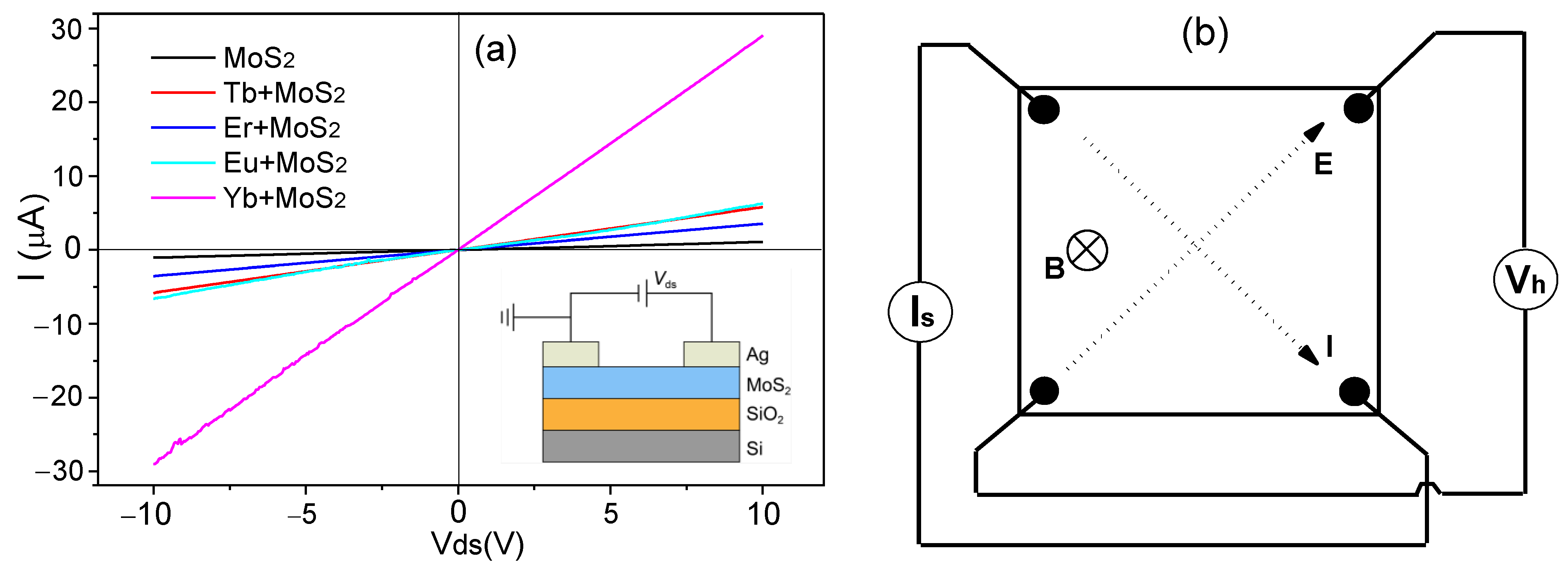
3.7. Electrical Properties

Figure 7a shows the I-V curves of the samples deposited on the SiO2/Si substrate after the annealing at 550 °C in Ar + 10% H2. The inset in Figure 7a is a schematic drawing of the sample in a circuit for I-V measurement (since no gate bias was applied to the device during the measurement, the gate electrode and its connections are not plotted). It can be seen that with applied bias, the electrical currents of the samples increased linearly (both forward and reverse) from 0 to 10 V, which means the samples had good Ohmic contacts and linear characteristics. The sheet resistance (Rs) of the film of the MoS2 sample was about 9.13 MΩ, while the resistance of the REs-doped samples was significantly smaller, especially for the Tb-doped MoS2 sample (0.34 MΩ). Similar phenomena were reported by Shi et al. [45] after Eu-doping of MoS2 film.
The carrier density (n), the electric mobility (μ) and the Hall coefficients (RH) of the samples were measured using a standard Hall effect setup with the geometry shown schematically in Figure 7b, and the measured data are given in Table 1. The majority of carriers in the undoped MoS2 sample were electrons with a density (n) of 6.17 × 10¹⁶/cm3. After RE (Yb, Tb and Er) doping, the n values of the respective samples increased by one or two orders of magnitude compared to the undoped one, and for the Eu-doped MoS2 sample, the majority of carriers were holes with a density of 1.44 × 1018 cm−3. The carrier mobility (μ) of the MoS2 did decrease with the RE doping. The mobility (μ) for the undoped MoS2 sample was 5.38 cm2/V·s, but was considerably smaller especially for the Yb3+ (0.653 cm2/V·s) and Er3+ (0.801 cm2/V·s) doping. This reduced μ was likely due to the increased scattering of carriers via the RE impurities and defects. The Hall coefficient (RH) (here, RHs is the sheet Hall coefficient) was calculated using the formula R H s = V h d I s B , where Vh is the Hall voltage as shown in Figure 7b, Is is the electrical current flowing through the sample film, B is 0.514 T and d is the thickness of the sample film. The signed value of RHs for the undoped MoS2 sample was −1.01 × 10⁴ (m2/C), and it increased to −54.3 (Yb3+), −860 (Tb3+) and −357 (Er3+) m2/C after RE-ion doping. Notably, the sign of RHs for the Eu-doped MoS2 sample was positive, which indicates a p-type semiconductor nature for the Eu-doped MoS2 sample. This is possibly tied to the first-principle calculation results of Maijdet et al. [46] on the change of MoS2 energy band structure via Eu doping. It was reported that the Mo-4d S-3p states that made up the top of the valence band of MoS2 became extended over a larger energy range, and the top of the valence band thus became unoccupied, as is typical for a p-type material. In this case, Eu had the lowest atomic number among the RE atoms we tested, and the Eu-4f band was below the Fermi level. The p-type doping could also have been due to sulphur interstitials being introduced in the MoS2 upon sputtering [47], since both EuS powder and S platelets were placed on the surface of the MoS2 target. We compared our results with some other groups’ electrical measurements, also shown in Table 1. One can see that the μ of our undoped MoS2 sample is larger than that of Ref. [11], also deposited via magnetron sputtering, but is much lower than those in Refs. [45,48], grown with the CVD method, although they have similar carrier densities (Ns).

4. Summary

In this work, we studied the structural, electrical and optical properties of RE-doped MoS2 films prepared using magnetron sputtering and subsequent 550 °C annealing in Ar + 10% H2. XRD and Raman spectra analysis indicated that the samples were crystallized with film thickness below 10 nm. XPS analysis indicated that most of the RE ions existed in a trivalent state in the films. The UV-vis absorption measurement indicated that compared to undoped MoS2 films, the optical bandgaps decreased from 1.57 to 1.31 eV after RE doping. The I-V measurements indicate that the electrical resistance and the mobility of the doped films decreased significantly, while the carrier density increased by one to two orders of magnitude. The sign of the Hall voltage indicates that the undoped and the Yb-, Tb- and Er-doped MoS2 samples were n-type semiconductors, while the Eu-doped MoS2 samples showed p-type characteristics. This study may be helpful to broaden the optoelectronic applications of these two-dimensional materials.

Author Contributions

Conceptualization, C.H.; methodology, C.H.; formal analysis, H.W. and T.G.F.; investigation, X.W., C.Z., G.W. and Y.L.; resources, M.Z.; writing—original draft preparation, C.H.; writing—review and editing, T.G.F.; supervision, C.H.; project administration, C.H.; funding acquisition, C.H. All authors have read and agreed to the published version of the manuscript.

Funding

This work is supported by the National Natural Science Foundation of China, No. 61775016.

Data Availability Statement

Data are contained within the article.

Acknowledgments

The authors wish to acknowledge the National Natural Science Foundation of China for the financial support.

Conflicts of Interest

The authors declare no conflict of interest.

References

  1. Wang, Q.H.; Kalantar-Zadeh, K.; Kis, A.; Coleman, J.N.; Strano, M.S.; Michael, S. Electronics and optoelectronics of two-dimensional transition metal dichalcogenides. Nat. Nanotechol. 2012, 7, 699. [Google Scholar] [CrossRef] [PubMed]
  2. Wang, X.M.; Xia, F.N. Stacked 2D materials shed light. Nat. Mater. 2015, 14, 264. [Google Scholar] [CrossRef]
  3. Lin, Z.; Liu, Y.; Halim, U.; Ding, M.; Liu, Y.; Wang, Y.; Jia, C.; Chen, P.; Duan, X.; Wang, C.; et al. Solution-processable 2D semiconductors for high-performance large-area electronics. Nature 2018, 562, 254. [Google Scholar] [CrossRef] [PubMed]
  4. Lin, X.; Yang, W.; Wang, K.; Zhao, W. Two-dimensional spintronics for low-power electronics. Nat. Electron. 2019, 2, 274. [Google Scholar] [CrossRef]
  5. Chen, P.; Han, W.; Zhao, M.; Su, J.W.; Li, Z.X.; Li, D.Y.; Pi, L.J.; Zhou, Z.; Zhai, T.Y. Recent advances in 2D rare earth materials. Adv. Funct. Mater. 2020, 31, 2008790. [Google Scholar] [CrossRef]
  6. Tong, L.; Huang, X.; Wang, P.; Ye, L.; Peng, M.; An, L.; Sun, Q.; Zhang, Y.; Yang, G.; Li, Z.; et al. Stable mid-infrared polarization imaging based on quasi-2D tellurium at room temperature. Nat. Commun. 2020, 11, 2308. [Google Scholar] [CrossRef]
  7. See for Example, MoS2 Materials, Physics, and Devices, Lecture Notes in Nanoscale Science and Technology; Wang, Z.M. (Ed.) Springer: Berlin/Heidelberg, Germany, 2014; Volume 21. [Google Scholar] [CrossRef]
  8. Baugher, B.W.H.; Churchill, H.O.H.; Yang, Y.F.; Jarillo-Herrero, P. Intrinsic electronic transport properties of high-quality monolayer and bilayer MoS2. Nano Lett. 2013, 13, 4212. [Google Scholar] [CrossRef]
  9. Duan, X.D.; Wang, C.; Pan, A.L.; Yu, R.Q.; Duan, X.F. Two-dimensional transition metal dichalcogenides as atomically thin semiconductors: Opportunities and challenges. Chem. Soc. Rev. 2015, 44, 8859. [Google Scholar] [CrossRef]
  10. Lopez-Sanchez, O.; Lembke, D.; Kayci, M.; Radenovic, A.; Kis, A. Ultrasensitive photodectors based on monolayer MoS2. Nat. Nanotechol. 2013, 8, 497. [Google Scholar] [CrossRef]
  11. Sirota, B.; Glavin, N.; Voevodin, A.A. Room temperature magnetron sputtering and laser annealing of ultrathin MoS2 for flexible transistor. Vacuum 2019, 160, 133. [Google Scholar] [CrossRef]
  12. Li, H.; Yin, Z.; He, Q.; Li, H.; Huang, X.; Lu, G.; Farm, D.W.H.; Tok, A.I.Y.; Zhang, Q.; Zhang, H. Fabrication of single- and multilayer MoS2 film-based field-effect transistors for sensing NO at room temperature. Small 2012, 8, 63. [Google Scholar] [CrossRef] [PubMed]
  13. Late, D.J.; Huang, Y.-K.; Liu, B.; Acharya, J.; Shirodkar, S.N.; Luo, J.; Yan, A.; Charles, D.; Waghmare, U.V.; Dravid, V.P.; et al. Sensing behavior of atomically thin-layered MoS2 transistors. ACS Nano 2013, 7, 4879. [Google Scholar] [CrossRef] [PubMed]
  14. Yu, Y.; Huang, S.-Y.; Li, Y.; Steinmann, S.N.; Yang, W.; Cao, L. Layer-dependent electrocatalysis of MoS2 for hydrogen evolution. Nano Lett. 2014, 14, 553. [Google Scholar] [CrossRef] [PubMed]
  15. Kim, S.; Konar, A.; Hwang, W.S.; Lee, J.H.; Lee, J.; Yang, J.; Jung, C.; Kim, H.; Yoo, J.B.; Choi, J.Y.; et al. High-mobility and low-power thin film transistors based on multilayer MoS2 crystals. Nat. Commun. 2012, 3, 1011. [Google Scholar] [CrossRef]
  16. Maddi, C.; Aswin, J.R.; Scott, A.; Aslam, Z.; Willneff, E.; Adarsh, K.N.V.D.; Jha, A. Structural, spectroscopic, and excitonic dynamic characterization in atomically thin Yb3+-doped MoS2 fabricated by femtosecond pulsed laser deposition. Adv. Optical. Mater. 2019, 7, 1900753. [Google Scholar] [CrossRef]
  17. Splendiani, A.; Sun, L.; Zhang, Y.; Li, T.; Kim, J.; Chim, C.-Y.; Galli, G.; Wang, F. Emerging photoluminescence in Monolayer MoS2. Nano Lett. 2010, 10, 1271. [Google Scholar] [CrossRef] [PubMed]
  18. Bai, G.X.; Yuan, S.G.; Zhao, Y.D.; Yang, Z.B.; Choi, S.Y.; Chai, Y.; Yu, S.F.; Lau, S.P.; Hao, J.H. 2D layered materials of rare-earth Er-doped MoS2 with NIR-to-NIR down-and up-conversion photoluminescence. Adv. Mater. 2016, 28, 7472. [Google Scholar] [CrossRef]
  19. Li, S.J.; Tian, S.D.; Yao, Y.; He, M.; Chen, L.; Zhang, Y.; Zhai, J.Y. Enhanced electrical performance of monolayer MoS2 with rare earth element Sm doping. Nanomaterials. 2021, 11, 769. [Google Scholar] [CrossRef]
  20. Yu, H.; Xu, J.; Guo, H.; Li, Y.R.; Liu, Z.Y.; Jin, Z.L. Synergistic effect of rare earth metal Sm oxides and Co1−xS on sheet structure MoS2 for photocatalytic hydrogen evolution. RSC Adv. 2017, 7, 56417. [Google Scholar] [CrossRef] [Green Version]
  21. Wang, H.G.; Wen, F.F.; Li, X.Y.; Gan, X.R.; Yang, Y.N.; Chen, P.; Zhang, Y. Cerium-doped MoS2 nanostructures: Efficient visible photocatalysis for Cr(VI) removal. Sep. Purif. Technol. 2016, 170, 190. [Google Scholar] [CrossRef]
  22. Magda, G.Z.; Peto, J.; Dobrik, G.; Hwang, C.; Biro, L.P.; Tapaszto, L. Exfoliation of large-area transition metal chalcogenide single layers. Sci. Rep. 2015, 5, 14714. [Google Scholar] [CrossRef] [PubMed]
  23. Coleman, J.N.; Lotya, M.; O’Neill, A.; Bergin, S.D.; King, P.J.; Khan, U.; Young, K.; Gaucher, A.; De, S.; Smith, R.J.; et al. Two-dimensional nanosheets produced by liquid exfoliation of layered materials. Science 2011, 331, 568. [Google Scholar] [CrossRef]
  24. Zeng, Z.Y.; Yin, Z.Y.; Huang, X.; Li, H.; He, Q.Y.; Lu, G.; Boey, F.; Zhang, H. Single-layer semiconducting nanosheets: High-yield preparation and device fabrication. Angew. Chem. Int. Ed. 2011, 50, 11093. [Google Scholar] [CrossRef]
  25. Shi, Y.; Li, H.N.; Li, L.J. Recent advances in controlled synthesis of two-dimensional transition metal dichalcogenides via vapor deposition techniques. Chem. Soc. Rev. 2015, 44, 2744. [Google Scholar] [CrossRef]
  26. Pyeon, J.J.; Kim, S.H.; Jeong, D.S.; Baek, S.H.; Kang, C.Y.; Kim, J.S.; Kim, S.K. Wafer-scale growth of MoS2 thin films by atomic layer deposition. Nanoscale 2016, 8, 10792. [Google Scholar] [CrossRef]
  27. Wu, S.F.; Huang, C.M.; Aivazian, G.; Ross, J.S.; Cobden, D.H.; Xu, X.D. Vapor-Solid Growth of High Optical Quality MoS2 Monolayers with Near-Unity Valley Polarization. ACS Nano 2013, 7, 2768. [Google Scholar] [CrossRef]
  28. Belikov, A.I.; Phyo, K.Z.; Kalinin, V.N.; Semochkin, A.I. Electronic and optical properties of MoS2 thin films deposited by magnetron sputtering studying. Proc. SPIE 2018, 11022, 110221F-1. [Google Scholar]
  29. Singh, R.; Tripathi, S. Structural and optical properties of few-layer MoS2 thin films grown on various substrates using RF sputtering process. J. Mater. Sci. Mater. Electron. 2019, 30, 7665. [Google Scholar] [CrossRef]
  30. Zhong, W.; Deng, S.B.; Wang, K.; Li, G.J.; Li, G.Y.; Chen, R.S.; Kwok, H.-S. Feasible route for a large area few-layer MoS2 with magnetron sputtering. Nanomaterials 2018, 8, 590. [Google Scholar] [CrossRef] [PubMed]
  31. Wong, W.C.; Ng, S.M.; Wong, H.F.; Cheng, W.F.; Mak, C.L.; Leung, C.W. Effect of post-annealing on sputtered MoS2 films. Solid-State Electron. 2017, 138, 62. [Google Scholar] [CrossRef]
  32. Li, X.L.; Han, W.P.; Wu, J.B.; Qiao, X.F.; Zhang, J.; Tan, P.H. Layer-number dependent optical properties of 2D materials and their application for thickness determination. Adv. Funct. Mater. 2017, 27, 1604468. [Google Scholar] [CrossRef]
  33. Li, X.L.; Qiao, X.; Han, W.-P.; Zhang, X.; Tan, Q.-H.; Chen, T.; Tan, P.-H. Determining layer number of two-dimensional flakes of transition-metal dichalcogenides by the Raman intensity from substrates. Nanotechnology 2016, 27, 145704. [Google Scholar] [CrossRef] [PubMed]
  34. Lu, X.; Utama, M.I.B.; Zhang, J.; Zhao, Y.; Xiong, Q. Layer-by-layer thinning of MoS2 by thermal annealing. Nanoscale 2013, 5, 8904. [Google Scholar] [CrossRef]
  35. Zhang, L.; Heng, C.L.; Zhao, C.N.; Su, W.Y.; Gao, Y.K.; Yin, P.G.; Finstad, T.G. On the structure and ultraviolet emission of terbium doped zinc oxide thin films on silicon after high temperature treatment. Results Phys. 2022, 32, 105121. [Google Scholar] [CrossRef]
  36. Huang, J.; Yang, L.; Liu, D.; Chen, J.J.; Fu, Q.; Xiong, Y.J.; Lin, F.; Xiang, B. Large-area synthesis of monolayer WSe2 on SiO2/Si substrate and its device applications. Nanoscale 2015, 7, 4193. [Google Scholar] [CrossRef]
  37. Haldar, D.; Ghosh, A.; Bose, S.; Mondal, S.; Ghorai, U.K.; Saha, S.K. Defect induced photoluminescence in MoS2 quantum dots and effect of Eu3+/Tb3+ co-doping towards efficient white light emission. Opt. Mater. 2018, 79, 12. [Google Scholar] [CrossRef]
  38. Ji, Q.Q.; Zhang, Y.F.; Gao, T.; Zhang, Y.; Ma, D.L.; Liu, M.X.; Chen, Y.B.; Qiao, X.F.; Tan, P.-H.; Kan, M.; et al. Epitaxial monolayer MoS2 on Mica with novel photoluminescence. Nano Lett. 2013, 13, 3870. [Google Scholar] [CrossRef]
  39. Ohno, Y. XPS studies of the intermediate valence state of Yb in (YbS)1.25CrS2. J. Electron Spectro. Relat. Phenom. 2008, 165, 1. [Google Scholar] [CrossRef]
  40. Vikraman, D.; Akbar, K.; Hussain, S.; Yoo, G.; Jang, J.-Y.; Chun, S.-H.; Jung, J.W.; Park, H.J. Direct synthesis of thickness-tunable MoS2 quantum dot thin layers: Optical, structural and electrical properties and their application to hydrogen evolution. Nano Energy 2017, 35, 101. [Google Scholar] [CrossRef]
  41. Eda, G.; Yamaguchi, H.; Voiry, D.; Fujita, T.; Chen, M.W.; Chhowalla, M. Photoluminescence from chemically exfoliated MoS2. Nano Lett. 2011, 11, 5111. [Google Scholar] [CrossRef]
  42. Tauc, J. Optical properties and electronic structure of amorphous Ge and Si. Mater. Res. Bull. 1968, 3, 37. [Google Scholar] [CrossRef]
  43. Mott, N.F.; Davis, E.A. Electronic Processes in Non-Crystalline Materials; Clarendon Press: Oxford, UK, 1979; ISBN 0-19-851288-0. [Google Scholar]
  44. Zhu, J.; Wu, J.; Sun, Y.; Huang, J.; Xia, Y.; Wang, H.; Wang, H.; Wang, Y.; Yi, Q.; Zou, G. Thickness-dependent bandgap tunable molybdenum disulfide films for optoelectronics. RSC Adv. 2016, 6, 110604. [Google Scholar] [CrossRef]
  45. Shi, W.L.; Li, Z.C.; Wang, L.; Wu, S.Y.; Zhang, G.N.; Meng, M.F.; Ma, X.Y. Photoelectric characteristics of rare earth element Eu-doped MoS2 thin films. Opt. Commun. 2018, 406, 50. [Google Scholar] [CrossRef]
  46. Majid, A.; Imtiaz, A.; Yoshiya, M. A density functional theory study of electronic and magnetic properties of rare earth doped monolayered molybdenum disulphide. J. Appl. Phys. 2016, 120, 142124. [Google Scholar] [CrossRef]
  47. Tao, J.G.; Chai, J.W.; Lu, X.; Wong, L.M.; Wong, T.I.; Pan, J.S.; Xiong, Q.H.; Chi, D.Z.; Wang, S.J. Growth of wafer-scale MoS2 monolayer by magnetron sputtering. Nanoscale 2015, 7, 2497. [Google Scholar] [CrossRef]
  48. Meng, M.F.; Ma, X.Y. Improving the photoelectric characteristics of MoS2 thin films by doping rare earth element erbium. Nanoscale Res. Lett. 2016, 11, 513. [Google Scholar] [CrossRef] [PubMed] [Green Version]
Figure 1. (a) The XRD spectra of the MoS2 samples deposited on SiO2/Si substrate after annealing at 550 °C for 30 min in N2 and Ar + 10% H2 ambience. (b,c) The XRD spectra of the RE-doped MoS2 samples deposited on the SiO2/Si substrate or the Al2O3 substrate and then annealed at 550 °C for 30 min in Ar + 10% H2 ambience. (d) A comparison of the average size of MoS2 nanoparticles in the samples.
Crystals 13 00308 g001
Figure 2. (a,b) The Raman spectra of the MoS2 and RE-doped MoS2 samples deposited on SiO2/Si and Al2O3 substrates, respectively, after 550 °C annealing in Ar + H2 gas ambience. (c) The separations (ΔK) between the E 2 g 1 and the A1g peaks for the samples. (d) The FWHMs of the A1g peaks of the samples deposited on the Al2O3 and the SiO2/Si substrates.
Crystals 13 00308 g002
Figure 3. Surface morphologies of the samples deposited on SiO2/Si substrate. (a) A.D. MoS2 and (b) MoS2 after the 550 °C annealing in Ar + H2 gas ambience. (cf) The SEM images of the RE (Er, Eu, Tb, Yb)-doped MoS2 samples after identical annealing.
Crystals 13 00308 g003
Figure 4. (a,b) Cross-sectional views of Eu-doped MoS2 samples after the 550 °C Ar + 10% H2 annealing. (c) HRTEM image of the MoS2 sample and (d) the sample’s diffraction pattern.
Crystals 13 00308 g004
Figure 5. The XPS spectra and deconvolutions for the samples deposited on SiO2/Si substrate after annealing at 550 °C in Ar + 10% H2. (a) S 2p (b) Mo 3d and S 2s, (c) Yb 4d for the Yb-doped MoS2, (d) Er 4d for the Er-doped MoS2, (e) Eu 4d for the Eu-doped MoS2 and (f) Tb 3d for the Tb-doped MoS2 sample.
Crystals 13 00308 g005
Figure 6. (a) Normalized absorption spectra of the samples deposited on Al2O3 substrates after annealing at 550 °C in Ar + 10% H2. (b) Tauc plot of the spectra, where the bandgaps of the samples were obtained via extrapolating the linear section to the hν axis.
Crystals 13 00308 g006
Figure 7. (a) The I–V curves of the samples deposited on SiO2/Si substrate after annealing at 550 °C in Ar + 10% H2. The inset in Figure 7a is a schematic drawing of the sample in a circuit for I–V measurement. (b) A standard Hall effect setup to measure the carrier density (n), the electric mobility (μ) and the Hall coefficients (RH) of the samples.
Crystals 13 00308 g007
Table 1. The electrical parameters of the films after 550 °C annealing in Ar + H2.
SampleN (cm−3)Ns (cm−2)μ (cm2/V-s)RHs (m2/C)RH (m3/C)
MoS2This work: −6.17 × 10¹⁶This work: −6.17 × 10¹⁰;
[42]: 1.55 × 10¹¹
This work: 5.38;
[11]: 0.024; [42]: 643;
[45]: 3996
This work: −1.01 × 10⁴[42]: 3.93;
[45]: 19.05
MoS2 + YbThis work: −1.15 × 10¹⁹ This work: −1.15 × 10¹³This work: 0.65This work: −54.3
MoS2 + TbThis work: −7.26 × 10¹⁷This work: −7.26 × 10¹¹This work: 2.74This work: −860
MoS2 + ErThis work: −1.75 × 10¹⁸This work: −1.75 × 10¹²This work: 0.80;
[45]: 5547
This work: −357[45]: 458.1
MoS2 + EuThis work: +1.44 × 10¹⁸This work: +1.44 × 10¹²;
[42]: 6.93 × 10¹¹
This work: 2.64;
[42]: 4950
This work: +433[42]: 21.33
Disclaimer/Publisher’s Note: The statements, opinions and data contained in all publications are solely those of the individual author(s) and contributor(s) and not of MDPI and/or the editor(s). MDPI and/or the editor(s) disclaim responsibility for any injury to people or property resulting from any ideas, methods, instructions or products referred to in the content.

