Article

Study on the Surface Structure of N-Doped 4H-SiC Homoepitaxial Layer Dependence on the Growth Temperature and C/Si Ratio Deposited by CVD

1
Institute of Wide Bandgap Semiconductors and Future Lighting, Academy for Engineering & Technology, Fudan University, Shanghai 200433, China
2
Shanghai Research Center for Silicon Carbide Power Devices Engineering & Technology, Fudan University, Shanghai 200433, China
3
Institute of Wide Bandgap Semiconductor Materials and Devices, Research Institute of Fudan University in Ningbo, Ningbo 315327, China
4
Department of Equipment Research for Wide Bandgap Semiconductor, Jihua Laboratory, Foshan 528200, China
*
Authors to whom correspondence should be addressed.
Crystals 2023, 13(2), 193; https://doi.org/10.3390/cryst13020193
Submission received: 28 December 2022 / Revised: 13 January 2023 / Accepted: 17 January 2023 / Published: 21 January 2023
(This article belongs to the Special Issue Semiconductor Material Growth, Characterization, and Simulation)

Abstract

:
The quality of the N-doped 4H-SiC homoepitaxial layers grown via hot-wall horizontal chemical vapor deposition (CVD) was evaluated at various C/Si ratios (1.0–1.2) and growth temperatures (1570–1630 °C). The microstructure and morphology of the epilayers were studied through a comparative analysis of the AFM patterns under different growth conditions. X-ray photoelectron spectroscopy and Raman spectroscopy revealed the quality of the 4H-SiC epilayers and the amount of N-doping. It was found that an increase in the C/Si ratio enabled obtaining a quite smooth epitaxial layer surface. Moreover, only the 4H-SiC crystal type was distinguished in the epilayers. In addition, the epitaxial quality was gradually improved, and the amount of defect-related C-C bonds significantly dropped from 38.7% to 17.4% as the N doping content decreased from 35.3% to 28.0%. An increase in the growth temperature made the epitaxial layer surface smoother (the corresponding RMS value was ~0.186 nm). According to the Raman spectroscopy data, the 4H-SiC forbidden mode E1(TO) in the epilayers was curbed at a higher C/Si ratio and growth temperature, obtaining a significant enhancement in epitaxial quality. At the same time, more N dopants were inserted into the epilayers with increasing temperature, which was opposite to increasing the C/Si ratio. This work definitively shows that the increase in the C/Si ratio and growth temperature can directly enhance the quality of the 4H-SiC epilayers and pave the way for their large-scale fabrication in high-power semiconductor devices.

1. Introduction

Silicon carbide (SiC) is characterized by a robust crystal structure, high-temperature resistance, outstanding conductivity, and favorable chemical stability [1,2,3,4]. In particular, its impressive conductive properties make SiC widely used in the semiconductor field, especially in electronic power devices. Meanwhile, tuning the content of impurities can change the electrical properties of silicon carbides. For example, n-type semiconductors are produced via the intentional introduction of nitrogen [5]. For instance, nearly 250 polytype isomers of SiC single crystals have been reported to date, of which the most common are the 3C, 4H, and 6H structures [6,7,8,9]. Compared with the other two types, the 3C-SiC configuration is unstable, making it difficult to grow large 3C-SiC ingots at a reasonable rate [8,9]. The intrinsic carrier concentration and electron mobility of the 4H-SiC are much higher than those of the 6H-SiC. Excessive electron mobility can result in a higher current density or a lower on-resistance with the same current density [10,11]. Moreover, the switching speed of the 4H VDMOS is slower than that of the 6H-SiC. As such, the 4H-SiC is suitable for the development of power devices.
In recent years, the 4H-SiC bulk single crystals have been extensively developed, and those of 6 inches have been put into industrial production. However, there are inevitable structural and surface defects in the substrate, which reduce the withstand voltage and carrier mobility of the material, greatly weakening the device’s performance [12,13,14,15,16,17,18,19,20]. To decrease the defect density, high-quality SiC epitaxial layers are often designed, which makes the whole plane flatter and hinders the emergence of defects, thereby ensuring the performance of appliances [21,22]. Generally, the epitaxial growth of other semiconductor materials such as silicon [23], sapphire [24], and titanium carbide [25] for cinnamon carbide only obtains 3C-SiC. Moreover, the large lattice mismatch between the layers and different coefficients of thermal expansion are conducive to the appearance of multiple defects. Therefore, using SiC single crystals as the substrates for homogeneous epitaxial growth has become a hot topic. At present, the preparation methods of SiC epitaxial films mainly include physical vapor transport (PVT) [26], liquid phase epitaxy (LPE) [27], sputtering, pulsed laser deposition (PLD) [28], molecular beam epitaxy (MBE) [29], and chemical vapor deposition (CVD) [30]. Among them, CVD is considered the most convenient epi-wafer deposition method for large-scale production owing to its relatively low growth temperature, good film uniformity, and easy-to-control growth process. The growth mechanism and key processes including the C/Si ratio [31], Cl/Si ratio [32,33,34,35], pressure [36,37], main hydrogen flow ratio [38], growth temperature [39,40], etc., of the epitaxial single-crystal 4H-SiC substrates are the basis for the growth of device-level epitaxial materials. By changing the temperature, the pressure of the growth process, and the proportion of the C2H4 and TCS (SiHCl3) to grow the carbon and silicon, the quality control of the 4H-SiC epitaxial layer can be achieved, thus reducing the macroscopic defect density, reducing the surface roughness, and improving the thickness and doping uniformity. There have been numerous types of research on advanced epitaxial technology. Hassan et al. [41] developed an over 100 µm/h growth rate process on 4-inch diameter wafers using chlorinated growth, which enabled them to obtain extremely smooth epilayers (RMS < 2 nm) with a very low surface defect density and high uniformity of thickness and doping. Lee et al. [40] produced 4H-SiC homoepitaxial layers onto 4°-off-axis Si-face and C-face substrates. According to the results, the high-quality and defect-free epilayers were obtained within a relatively low temperature range of 1320–1440 °C on the Si-face substrates and at 1500 °C on the C-face substrates at a low source flow rate of 5–10 sccm (the best result of the RMS roughness was 0.2–0.3 nm at a temperature of 1440 °C and flow rate of 10 sccm). Tsuchida et al. [42] developed a single-wafer vertical-type epitaxial reactor for 4-inch diameter wafers, which realized high-speed wafer rotation, thus greatly enhancing the growth rates and the uniformity of thickness and doping, as well as rather a smooth surface (RMS = 0.21 nm). High-quality epitaxial wafers are the basis of high-performance power devices. Therefore, exploring the technique for enhancing the epitaxial quality is a matter of great importance.
In the present study, emphasis is placed on the influence of the C/Si ratio and growth temperature on the quality of the SiC epilayer grown using CVD. These comparative experiments were conducted to comprehensively analyze the effects of the growth process on the chemical composition and microstructure of the epilayers. A series of characterization methods were utilized for surface analysis, namely, X-ray spectroscopy (XPS), atomic force microscopy (AFM), and Raman spectroscopy. Specifically, the evolution of the epilayers’ microstructure, polytype, and surface morphology was monitored. The surface chemistry analysis of the intrinsic defects was performed by the C 1 s of the XPS spectra. The comparative study revealed the internal relationship between the process parameters and the material properties, thus providing an in-depth understanding of the epitaxial growth mechanism with the aim of improving the quality of the epilayers in industrial production.

2. Experimental Procedures

2.1. Sample Preparation

4H-SiC homoepitaxial layers were grown on 4°-off-axis 4H-SiC Si-face substrates using a homemade low-pressure horizontal hot-wall chemical vapor deposition (CVD) setup equipped with an active gas injection system that allowed the H2, C2H4, TCS, and N2 flows to be modulated along the central main circuit and the adjacent side circuits. Before reaching the growth temperature in the reactor, the SiC substrates were etched in situ in an H2 atmosphere for 10 min. Then, accompanied by the H2 carrier gas at the total flux of 120 slm, the precursors (C2H4 and TCS) were introduced into the reaction chamber in a certain proportion, which determined the C/Si ratio. The growth pressure and the growth temperature were set to 100 mbar and 1570–1630 °C, respectively. The flux of the dopant N2 source for highly doped (~1017 cm−3) n-type SiC epilayers was maintained at 250 sccm. According to the above process parameters, five groups of comparative experiments were conducted. The C/Si ratios and growth temperatures are listed in Table 1.

2.2. Characterization

The prepared epilayers were analyzed by various characterization methods. The root mean square roughness (RMS) values and topography mapping were determined using a Bruker Dimension Icon AFM system with 1 µm × 1 µm scans. The polytype structure of the SiC epilayers was investigated at room temperature via backscattering Raman spectroscopy in the wavenumber range of 500–1200 cm−1 by means of a LabRAM HR (HORIBA, Tokyo, Japan)Raman spectrometer paired with an Ar+ laser (532 nm). The XPS (SPECS) measurements were carried out to characterize the surface chemical composition of the epilayers.

3. Results and Discussion

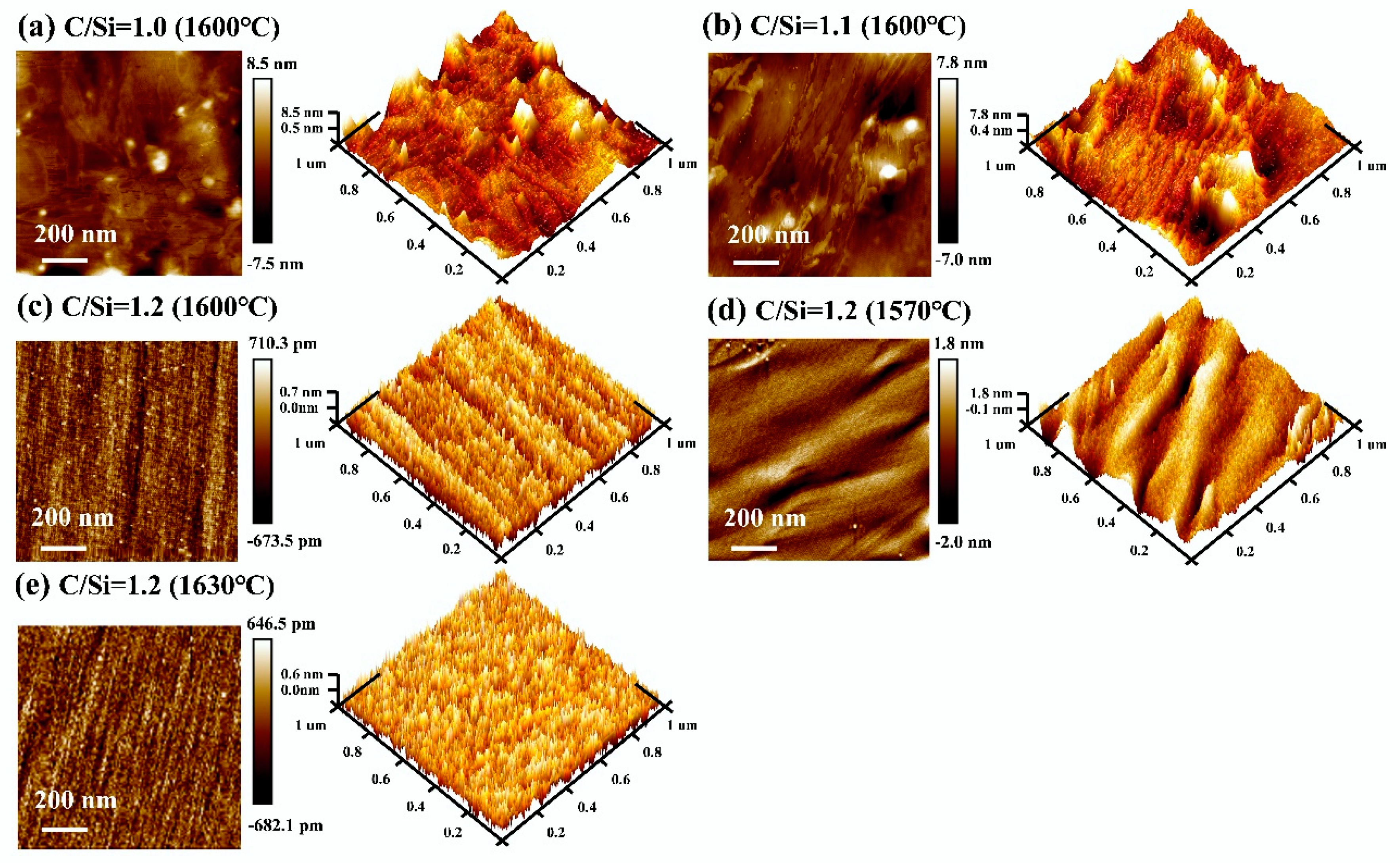
3.1. The Surface Morphology of the N-Doped 4H-SiC Epilayers

To directly observe the microstructure evolution of the N-doped 4H-SiC epilayers grown under different conditions, AFM mapping was conducted. Figure 1 depicts the 2D and 3D surface morphology images of the 4H-SiC homoepitaxial layers. The grain distributions of the different growth parameters were evaluated, and the root mean square (RMS) values are listed in Table 1. Figure 1a–c show the typical AFM images of the as-grown 4H-SiC homoepitaxial layers with the uniform increase in the C/Si ratio at 1600 °C. At C/Si = 1.0, small sporadic distribution grains appeared. As the ratio increased, the volume of 4H-SiC grains increased gradually on the surface of the epilayers and was distributed along the steps, which vividly and intuitively proved the combination of island-like and step-flow growth modes in the 4H-SiC homoepitaxial growth. Meanwhile, the crystallinity and surface quality of the 4H-SiC epilayers were relatively poor. By further increasing the C/Si ratio, the grains entirely covered the epilayers, forming a perfectly flat surface. According to Table 1, when the C/Si ratio increased from 1.0 to 1.2, the RMS values decreased monotonically from 1.91 to 0.194 nm. Therefore, the 4H-SiC epitaxial growth strongly depended on the C/Si ratio. In addition, the growth temperature (GT) is an essential factor causing microchanges in the surface morphology [39,41]. Figure 1c–e display the surface topography of the epilayers within the temperature range of 1570–1630 °C at the same C/Si ratio (1.2), revealing the correlation between the growth temperatures and the morphology of the epitaxial layer. The coexistence of the step-flow and island-like growth modes was evident from Figure 1d, and relatively large grains were formed on the surface at GT = 1570 °C. As the growth temperature increased, the surface atoms gained enough energy to migrate and enhance the nucleation. Thus, quite a flat surface could be obtained at higher temperatures. In particular, the value of the RMS was 0.186 nm at GT = 1630 °C.

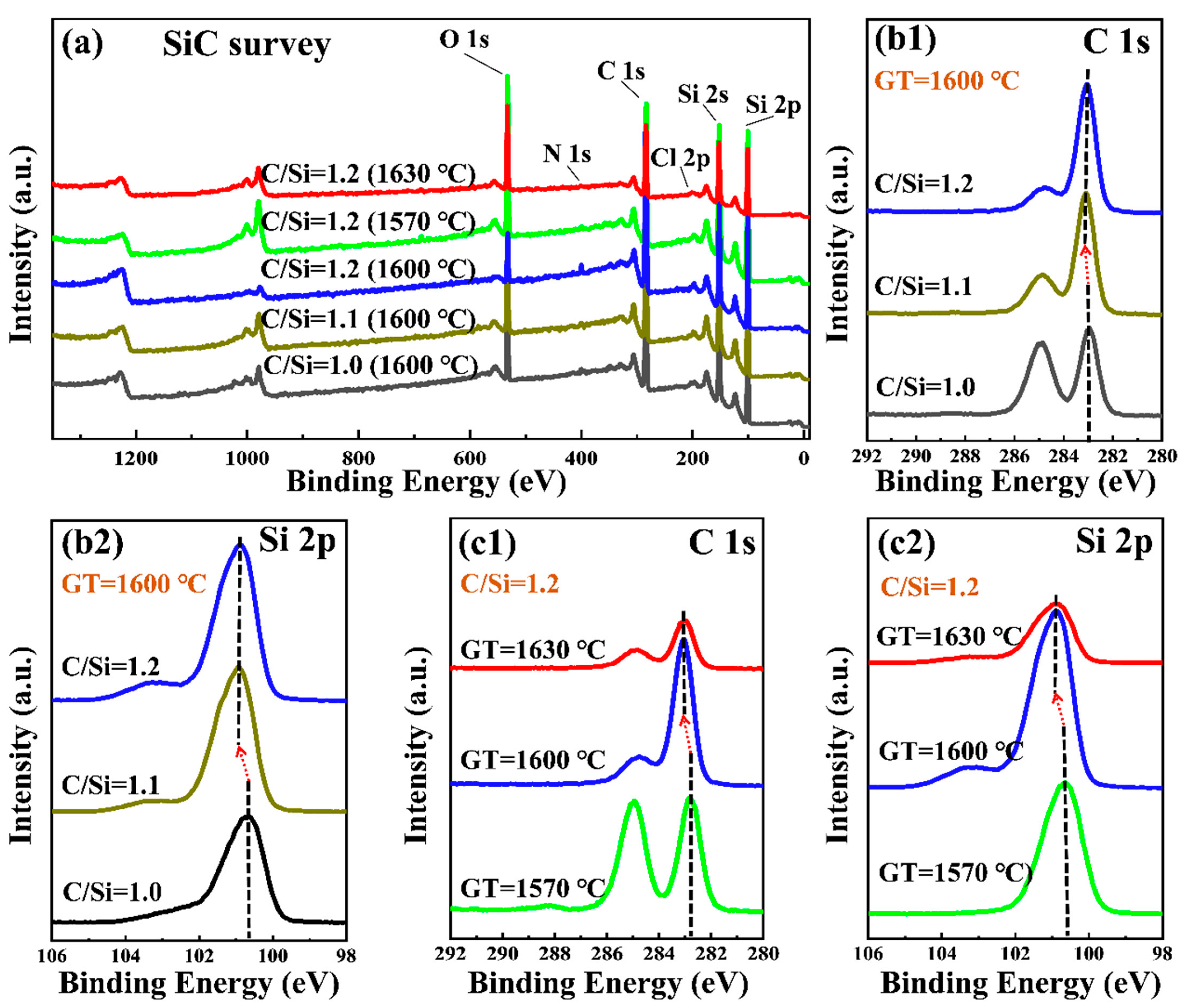
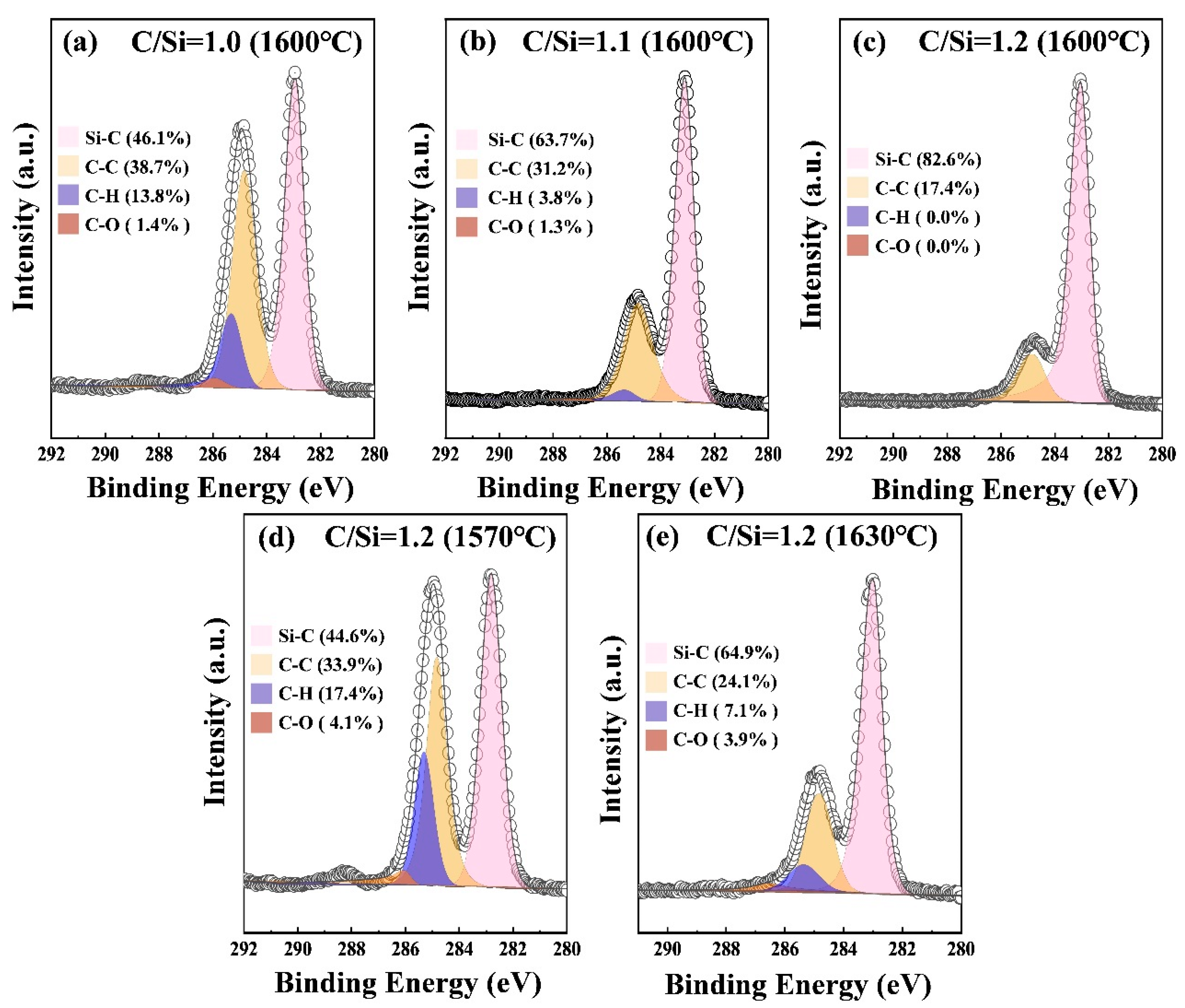
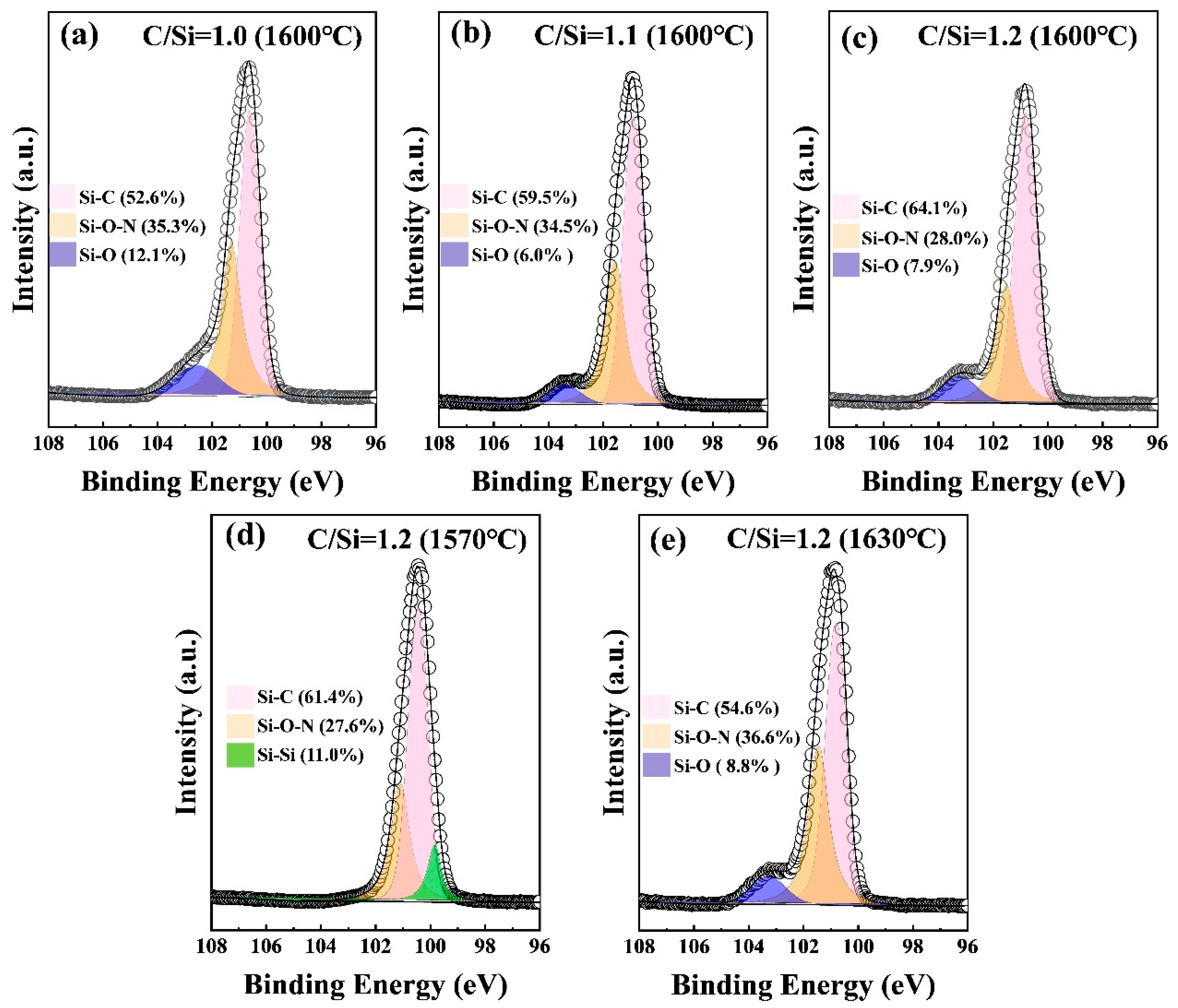
3.2. Chemical Composition Analysis

To gain a better insight into the elemental composition and defects of the N-doped 4H-SiC epilayers, XPS measurements were performed. The survey XPS spectra (Figure 2a) disclosed the presence of elemental C, O, Si, and N on the epilayer surface. The detailed atomic proportion is summarized in Table 2. To quantitatively investigate the influence of the C/Si ratio and growth temperature on the chemical properties of the 4H-SiC epilayers in detail, high-resolution C 1s and Si 2p spectra were further acquired. Figure 3 depicts the C 1 s core-level XPS curve fitting using mixed Gaussian and Lorentzian line shapes after subtracting a Shirley background. In addition to the major Si-C bond, several contaminants including C-C, C-H, and C-O bonds were detected as well [43,44,45]. After curve fitting, all the XPS spectra were calibrated with respect to the C-C peak at 284.8 eV.
As seen from Figure 3 and Figure 4, the proportions of the Si-C bonds in both the C 1 s and Si 2p spectra tended to rise with an increase in the C/Si ratio, meaning the continuous formation of SiC in the epilayers. The existence of the C-C bonds was ascribed to defects [42,46,47]. Moreover, according to Figure 3a–c, the amount of surface-dominant C-C contaminant species decreased with the increase in the C/Si ratio. In Figure 4a–c, the amount of dopant-related Si-O-N bonds tended to have lower proportions as the C/Si ratio increased. This was due to the gradually weakening N-site competition with the increasing C/Si ratio [48], which corresponded to the results in Table 2. Moreover, there were few O atoms (Statistics in Table 2) on the surface at 1570 °C, which was evident from the disappearance of the Si-O bond related peak near 103.0 eV [49]. The band attributed to the Si-Si bonds was identified at 99.8 eV, which indicated the presence of scarce Si droplets on the surface at relatively low temperatures [50]. With the increase in the O contents at higher temperature (as shown in Table 2), the Si-O bonds increased, while the Si-Si bonds disappeared. In addition, according to Figure 3c–d and Figure 4c–d, the proportions of the Si-C bonds in the C 1 s and Si 2p spectra increased at the temperatures of 1570–1600 °C, while they decreased at higher temperatures. A significant increase in the amount of Si-C bonds at the beginning indicated that the formation of SiC was dominant at this stage. However, once the temperature reached 1630 °C, the quantity of the Si-C bonds decreased from 62.8% to 54.6%. So, more N impurities occupied the C sites (NC) while releasing abundant vacancies in SiC [51,52]. Therefore, the reduction in number of Si-C bonds could be reasonably clarified at the higher growth temperatures.
In addition, the C 1 s and Si 2p peak positions both shifted in a regular manner under different growth parameters (shown with red dotted arrows and black dashed lines in Figure 2b,c). The existence of the C-C bonds was attributed to defects, which often induce a certain deviation of the binding energy [53]. With the increase in the C/Si ratio from 1.0 to 1.2, the quantities of C-C bonds were found to be 38.7%, 31.2%, and 17.4%, respectively. The decrease in the defect-related C-C bonds generally results in a slight shift toward the higher binding energies, which was consistent with the movement of the C 1 s and Si 2p spectra in Figure 2b1,b2. With the increase in the growth temperature from 1570 °C to 1630 °C, the proportions of the C-C bonds decreased from 33.9% to 17.4% and then increased to 24.1%. Therefore, a slight shift occurred in the binding energies of the C 1 s and Si 2p spectra, as shown in Figure 2c1,c2.

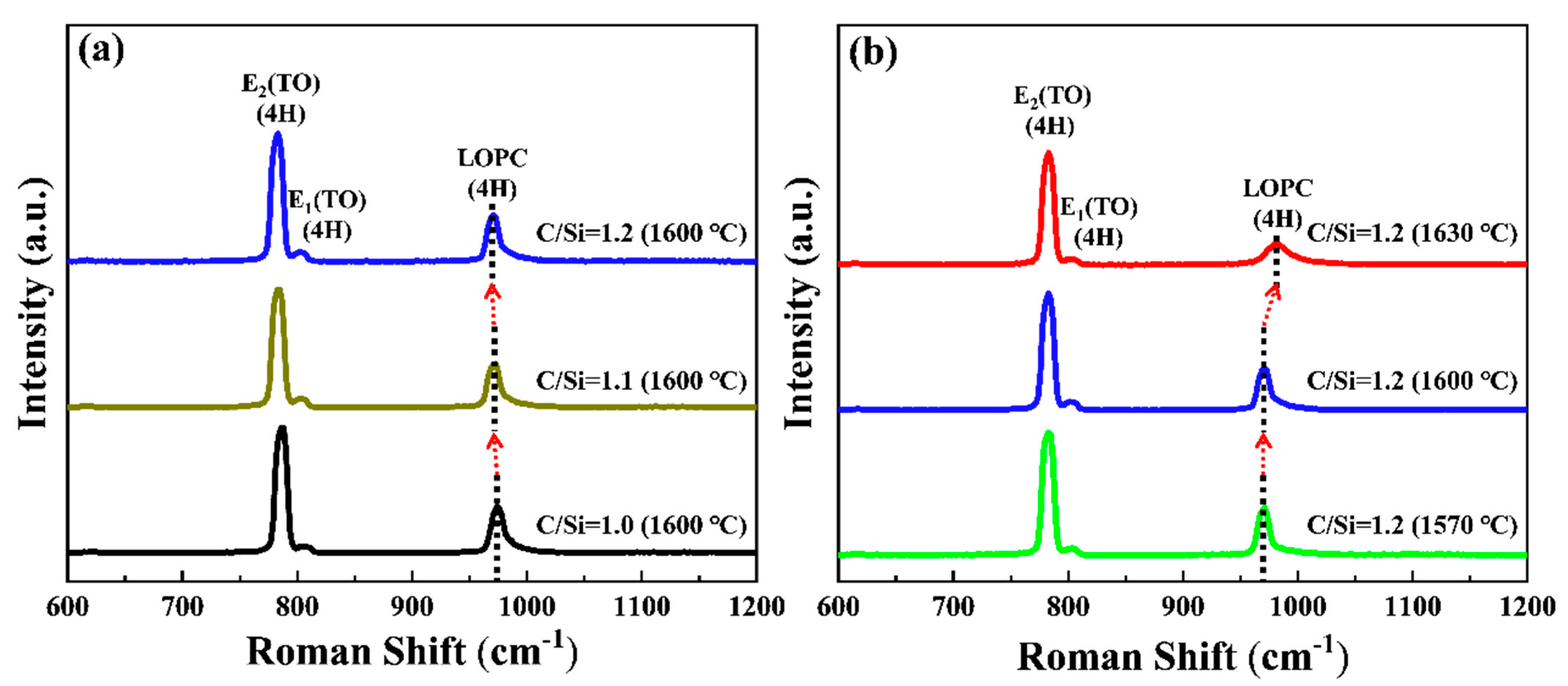
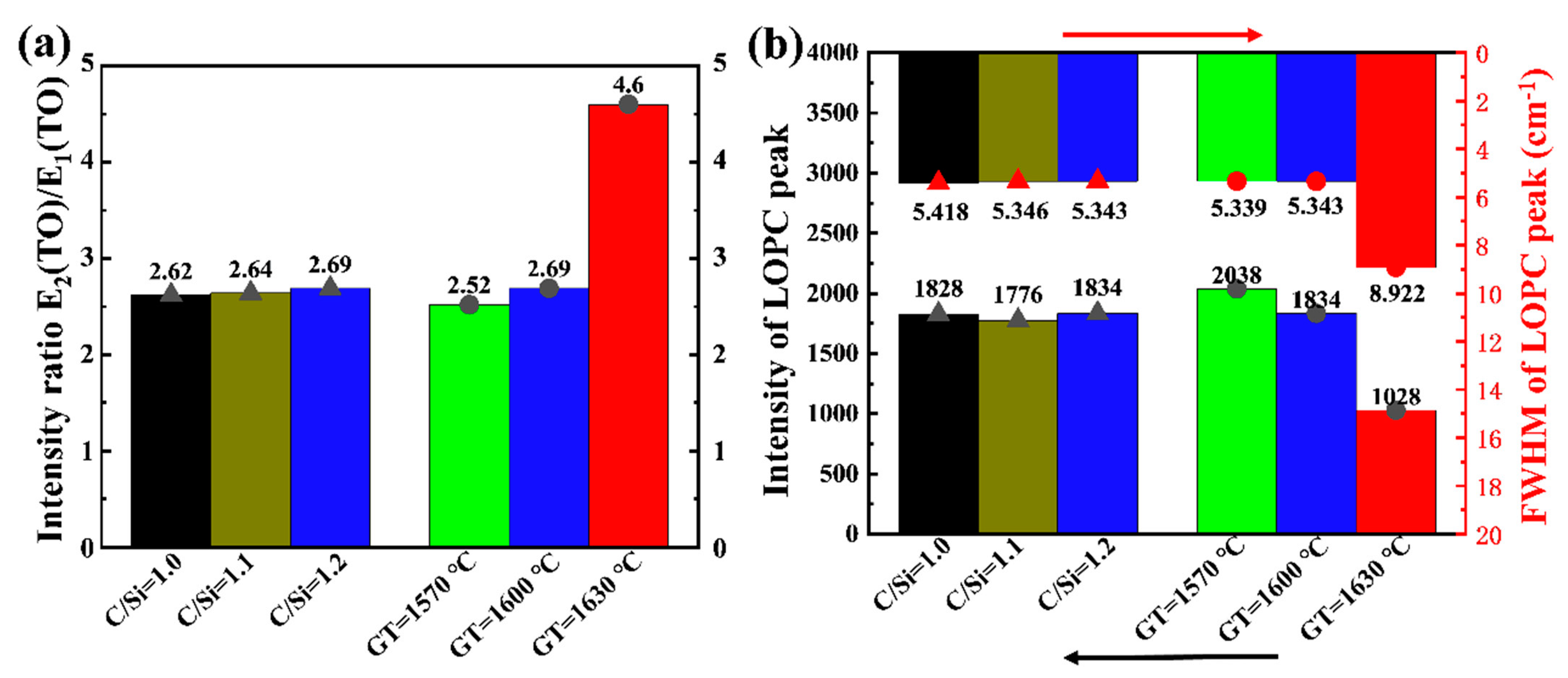
3.3. Polytype Control

To confirm the polytypes of the five 4H-SiC epilayers, the Raman measurements were conducted at a 532 nm laser excitation wavelength. As shown in Figure 5, three relatively strong Raman peaks were distinguished in the epitaxial layers in the range of 600–1200 cm−1. Among them, the first two peaks were assigned to transversal (TO) optic modes [54]. The other peak at 970 cm−1 was ascribed to the longitudinal phonon–plasmon coupling (LOPC) mode [46]. It is worth mentioning that for the 4H-SiC, the E1(TO) mode is forbidden by the Raman selection rules [55,56]. Since the El (TO) and E2(TO) modes come from lattice vibrations in different directions, they can reflect the degree of crystal orientation irregularities. Therefore, the E2(TO)/E1(TO) intensity ratio is considered the indicator of the crystal quality of the epilayers [56]. Specifically, a higher intensity ratio means fewer defects and better crystal quality. In Figure 6a, the intensity ratio rose with the increase in the C/Si ratio and the growth temperature, which indicated the improvement in the quality of the 4H-SiC epilayers. In general, the LOPC peak is related to the dopant concentration [57]. In particular, the large dopant content is conducive to the interaction between atoms and crystal cells. With the increase in the doping concentration, the phonons increase, and the scattering probability increases, but the phonon lifetime decreases. In this work, as the C/Si ratio increased, there was a slight redshift in the LOPC peaks (see Figure 5a). This corresponded to the gradual decrease in the N dopant concentration, as discussed above. In contrast, more prominent features emerged with the increase in the growth temperature. For example, the LOPC peaks became wider (their FWHM varied between 5.339 and 8.922 cm−1 in Figure 6b and moved toward the higher frequencies in Figure 5b). The scattering field intensity decrease is shown in Figure 6b. All these characteristics at higher growth temperatures demonstrated the increase in the N doping concentration. The scattering field intensity decrease is shown in Figure 6b. These results confirm the aforementioned XPS analysis.

4. Conclusions

In this work, N-doped 4H-SiC homoepitaxial layers were deposited using CVD at various growth temperatures and C/Si ratios. The influence of the C/Si ratio and growth temperature on the quality of epilayers was investigated via AFM, XPS, and Raman spectroscopy. It was found that the micromorphology strongly depended on the C/Si ratio and growth temperature. As the C/Si increased from 1.0 to 1.2, the value of the RMS decreased dramatically from 6.06 to 0.238 nm. In addition, the flatness of the surface was improved (RMS~0.217 nm) by increasing the growth temperature from 1570 to 1630°C. According to the XPS analysis, with the increase in the C/Si ratio, the amount of defect-related C-C bonds decreased significantly from 38.7% to 17.4%, simultaneously inducing SiC nucleation. In terms of the relationship between the temperature and the epitaxial quality, the higher temperature promoted the formation of the Si-C species but concurrently generated more vacancies due to the enhancement of the N doping efficiency. As for the polytypes, only 4H-SiC species were detected without any other crystal forms in the epilayers. The E2(TO)/E1(TO) intensity ratio increased with the increase in the C/Si ratio and growth temperature, implying the improvement in the epilayer quality. In addition, according to the shift in the LOPC peaks, the change in the N-doping concentration was consistent with the XPS data. Therefore, this report, on the one hand, provides a deeper understanding of the epitaxial growth physical mechanism and some theoretical support for the subsequent control of defects and doping concentration. On the other hand, it strives to extend the application of SiC in the field of power electronics.

Author Contributions

Z.T.: Methodology, Data curation, Writing—original draft, Formal analysis. L.G.: Validation, Investigation, Formal analysis, Data curation. H.M.: Conceptualization, Supervision, Funding acquisition, Project administration, Writing—review and editing. K.D.: Validation, Investigation. Q.L.: Supervision, Resources. N.Z.: Investigation, Writing—review and editing. J.H.: Data curation, Writing—review and editing. J.F.: Project administration, Investigation, Supervision. All authors have read and agreed to the published version of the manuscript.

Funding

This research was funded by National Natural Science Foundation of China (No.11804055 and 52275559), Science and Technology Innovation Plan of Shanghai Science and Technology Innovation Plan of Shanghai Science and Technology Commission (No. 21DZ1100800, 20501110700, and 20501110702), Taiyuan Science and Technology Development Funds (Jie Bang Gua Shuai Program). The APC was funded by Taiyuan Science and Technology Development Funds (Jie Bang Gua Shuai Program).

Data Availability Statement

The data that support the findings of this study are available from the corresponding author, H.M, upon reasonable request.

Acknowledgments

This work was supported by the National Natural Science Foundation of China (No. 11804055 and 52275559), the Science and Technology Innovation Plan of the Shanghai Science and Technology Commission (No. 21DZ1100800, 20501110700, and 20501110702), and the Taiyuan Science and Technology Development Funds (Jie Bang Gua Shuai Program).

Conflicts of Interest

The authors declare that they have no known competing financial interests or personal relationships that could have appeared to influence the work reported in this paper.

References

  1. Pensl, G. Electrical and optical characterization of SiC. Physica B 1993, 185, 264–283. [Google Scholar] [CrossRef]
  2. Misra, A.K. Chemical Compatibility Issues Related to Use of Copper as an Interfacial Layer for SiC Fiber Reinforced Ti3Al+Nb Composite. NASA Contractor Report; NASA: Washington, DC, USA, 1991. [Google Scholar]
  3. Casady, J.B.; Johnson, R.W. Status of silicon carbide (SIC) as a wlde-bandgap semiconductor for high-temperature applications: A review. Solid-State Electron. 1996, 39, 1409–1422. [Google Scholar] [CrossRef]
  4. Mantooth, H.A.; Peng, K.; Santi, E.; Hudgins, J.L. Modeling of Wide Bandgap Power Semiconductor Devices—Part I. IEEE Trans. Electron Devices 2014, 62, 423–433. [Google Scholar] [CrossRef]
  5. Li, S.; Li, J.; Su, Q.; Liu, X.; Zhao, H.; Ding, M. Enhanced n-type conductivity of 6H-SiC nanowires by nitrogen doping. Micro Nano Lett. 2019, 14, 999–1002. [Google Scholar]
  6. Presser, V.; Nickel, K.G. Silica on Silicon Carbide. Crit. Rev. Solid State Mater. Sci. 2008, 33, 1–99. [Google Scholar] [CrossRef]
  7. Okamoto, M.; Kosugi, R.; Nakashima, S.; Nakashima, S.; Fukuda, K.; Arai, K. Deep UV excitation Raman spectroscopy of homoepitaxial 4H-SiC films grown by microwave plasma chemical vapor deposition. Materials Science Forum 2004, 457, 629–632. [Google Scholar] [CrossRef]
  8. Leone, S.; Beyer, F.; Henry, A.; Kordina, O.; Janzén, E. Chloride-based CVD of 3C-SiC epitaxial layers on 6H(0001) SiC. Phys. Status Solidi (RRL)—Rapid Res. Lett. 2010, 4, 305–307. [Google Scholar] [CrossRef]
  9. Soueidan, M.; Ferro, G. A Vapor–Liquid–Solid Mechanism for Growing 3C-SiC Single-Domain Layers on 6H-SiC(0001). Adv. Funct. Mater. 2006, 16, 975–979. [Google Scholar] [CrossRef]
  10. Gao, Y.Q.; Zhang, H.Y.; Zong, Y.M.; Wang, H.H.; Guo, J.Q.; Raghothamachar, B.; Dudley, M.; Wang, X.J. 150 mm 4H-SiC Substrate with Low Defect Density. Mater. Sci. Forum 2016, 858, 41–44. [Google Scholar] [CrossRef]
  11. Liu, B.; Sun, G.-S.; Liu, X.-F.; Zhang, F.; Dong, L.; Zheng, L.; Yan, G.-G.; Liu, S.-B.; Zhao, W.-S.; Wang., L.; et al. Fast Homoepitaxial Growth of 4H-SiC Films on 4° off-Axis Substrates in a SiH4-C2H4-H2 System. Chin. Phys. Lett. 2013, 30, 128101. [Google Scholar] [CrossRef]
  12. Philip, G.; Neudeck, A.P. Performance Limiting Micropipe Defects in Silicon Carbide Wafers. IEEE Electron. Device Lett. 1994, 15, 63–65. [Google Scholar]
  13. Kamata, I.; Zhang, X.; Tsuchida, H. Photoluminescence of Frank-type defects on the basal plane in 4H–SiC epilayers. Appl. Phys. Lett. 2010, 97, 172107. [Google Scholar] [CrossRef]
  14. Song, H.; Rana, T.; Sudarshan, T.S. Investigations of defect evolution and basal plane dislocation elimination in CVD epitaxial growth of silicon carbide on eutectic etched epilayers. J. Cryst. Growth 2011, 320, 95–102. [Google Scholar] [CrossRef]
  15. Wada, K.; Terao, T.; Miyase, T.; Hori, T.; Doi, H.; Furumai, M. High-Quality 6-inch SiC Epitaxial Wafer “EpiEra”. Electronics 2018, 87, 54–58. [Google Scholar]
  16. Feng, G.; Suda, J.; Kimoto, T. Characterization of major in-grown stacking faults in 4H-SiC epilayers. Phys. B: Condens. Matter 2009, 404, 4745–4748. [Google Scholar] [CrossRef]
  17. Konstantinov, A.O.; Hallin, C.; Pecz, B.; Kordina, O.; Janzen, E. The mechanism for cubic SiC formation on off-oriented substrates. J. Cryst. Growth 1997, 178, 495–504. [Google Scholar] [CrossRef]
  18. Lendenmann, H.; Bergman, P.; Dahlquist, F.; Hallin, C. Degradation in SiC Bipolar Devices: Sources and Consequences of Electrically Active Dislocations in SiC. Mater. Sci. Forum 2003, 433, 901–906. [Google Scholar] [CrossRef]
  19. Senzaki, J.; Shimozato, A.; Kajima, K.; Aryoshi, K.; Kojima, T.; Harada, S.; Okumura, H. Electrical Properties of MOS Structures on 4H-SiC (11-20) Face. Mater. Sci. Forum 2013, 740, 621–624. [Google Scholar] [CrossRef]
  20. Han, S.Y.; Kim, N.K.; Kim, E.D.; Lee, J.L. Effects of Interfacial Reactions on Electrical Properties of Ni Ohmic Contacts on n-Type 4H-SiC. Mater. Sci. Forum 2002, 389, 897–900. [Google Scholar] [CrossRef]
  21. Spera, M.; Corso, D.; Di Franco, S.; Greco, G.; Severino, A.; Fiorenza, P.; Giannazzo, F.; Roccaforte, F. Effect of high temperature annealing (T > 1650 °C) on the morphological and electrical properties of p-type implanted 4H-SiC layers. Mater. Sci. Semicond. Process. 2019, 93, 274–279. [Google Scholar] [CrossRef] [Green Version]
  22. Rupp, R.; Makarov, Y.N.; Behner, H.; Wiedenhofer, A. Silicon Carbide Epitaxy in a Vertical CVD Reactor: Experimental Results and Numerical Process Simulation. Phys. Status Solidi 1997, 202, 281–304. [Google Scholar] [CrossRef]
  23. Li, J.; Zhao, Y.; Liu, X.; Sun, G.; Wang, L.; Zhao, W.; Luo, M.; Zeng, Y.; Li, J. Fast Epitaxy of 3C-SiC Grown on Si Substrate. Chin. Inst. Electron. 2007, 28, 218–220. [Google Scholar]
  24. Sun, G.S.; Li, J.M.; Luo, M.C.; Zhu, S.R.; Wang, L.; Zhang, F.F.; Lin, L.Y. Epitaxial growth of SiC on complex substrates. J. Cryst. Growth 2001, 227, 811–815. [Google Scholar] [CrossRef]
  25. Chaudhuri, J.; Thokala, R.; Edgar, J.H.; Sywe, B.S. Sywe X-ray double crystal and X-ray topographic characterization of silicon carbide thin films on silicon, titanium carbide, 6H-silicon carbide, and aluminum nitride/sapphire substrates. Thin Solid Film. 1996, 274, 23–30. [Google Scholar] [CrossRef]
  26. Khlebnikov, Y.; Khlebnikov, I.; Parker, M.; Sudarshan, T.S. Local epitaxy and lateral epitaxial overgrowth of SiC. J. Cryst. Growth 2001, 233, 112–120. [Google Scholar] [CrossRef]
  27. Syrkin, A.; Dmitriev, V.; Kovalenkov, O.; Bauman, D.; Crofton, J. Liquid-Phase Epitaxial Growth of Heavily Doped Al p-Type Contact Layers for SiC Devices and Resulting Ohmic Contacts. Mater. Sci. Forum 2002, 389, 291–294. [Google Scholar] [CrossRef]
  28. Schlaf, M.; Sands, D.; Key, P.H. Optical characterisation of pulsed laser deposited SiC films. Appl. Surf. Sci. 2000, 154, 83–88. [Google Scholar] [CrossRef]
  29. Komatz, M.; Matsuishi, K.; Hong, S.K.; Yao, T. Homoepitaxial SiC deposition by MBE with Si and monomethlysilane. Phys. Status Solidi C 2006, 3, 571–574. [Google Scholar] [CrossRef]
  30. Chen, Y.; Kimoto, T.; Takeuchi, Y.; Malhan, K.R.; Matsunami, H. Homoepitaxy of 4H-SiC on Trenched (0001) Si Face Substrates by Chemical Vapor Deposition. Jpn. J. Appl. Phys. 2004, 43, 4105–4109. [Google Scholar] [CrossRef]
  31. Yan, G.G.; He, Y.W.; Shen, Z.W.; Cui, Y.X.; Li, J.T.; Zhao, W.S.; Wang, L.; Liu, X.F.; Zhang, F.; Sun, G.S.; et al. Effect of C/Si ratio on growth of 4H-SiC epitaxial layers on on-axis and 4° off-axis substrates. J. Cryst. Growth 2020, 531, 125362. [Google Scholar] [CrossRef]
  32. Leone, S.; Pedersen, H.; Henry, A.; Kordina, O.; Janzén, E. Thick homoepitaxial layers grown on on-axis Si-face 6H- and 4H-SiC substrates with HCl addition. J. Cryst. Growth 2009, 312, 24–32. [Google Scholar] [CrossRef]
  33. Kotamraju, S.; Krishnan, B.; Melnychuk, G.; Koshka, Y. Low-temperature homoepitaxial growth of 4H–SiC with CH3Cl and SiCl4 precursors. J. Cryst. Growth 2010, 312, 645–650. [Google Scholar] [CrossRef]
  34. Liu, X.F.; Yan, G.G.; Liu, B.; Shen, Z.W.; Wen, Z.X.; Chen, J.; Zhao, W.S.; Zhang, F.; Sun, G.S.; Zeng, Y.P. Process optimization for homoepitaxial growth of thick 4H-SiC films via hydrogen chloride chemical vapor deposition. J. Cryst. Growth 2018, 504, 7–12. [Google Scholar] [CrossRef]
  35. Li, Z.; Ju, T.; Niu, Y. Study on the Chloride-based 4H-SiC Epi-layer. Smart Grid. 2016, 4, 649–652. [Google Scholar]
  36. Christopher, S.; Roper, C.C.; Roger, T. Howe, and Roya Maboudian. Silicon Carbide Thin Films using 1,3-Disilabutane Single Precursor for MEMS Applications—A Review. ECS Trans. 2006, 3, 267–280. [Google Scholar]
  37. Zhang, T.; Li, Y.; Feng, Q.; Zhang, Y.; Ning, J.; Zhang, C.; Zhang, J.; Hao, Y. Effects of growth pressure on the characteristics of the β-Ga2O3 thin films deposited on (0001) sapphire substrates. Mater. Sci. Semicond. Process. 2021, 123, 105572. [Google Scholar] [CrossRef]
  38. Li, Y.; Zhao, Z.; Zhu, Z.; Li, Z. Aluminum doping property in SiC epilayers grown at high growth rate using chloride-based CVD. J. Mater. Sci. Mater. Electron. 2015, 26, 2338–2342. [Google Scholar] [CrossRef]
  39. Niu, Y.; Tang, X.; Sang, L.; Li, Y.; Kong, L.; Tian, L.; Tian, H.; Wu, P.; Jia, R.; Yang, F.; et al. The influence of temperature on the silicon droplet evolution in the homoepitaxial growth of 4H-SiC. J. Cryst. Growth 2018, 504, 37–40. [Google Scholar] [CrossRef]
  40. Lee, H.; Kim, H.; Seo, H.S.; Lee, D.; Kim, C.; Lee, S.; Kang, H.; Heo, J.; Kim, H.J. Comparative Study of 4H-SiC Epitaxial Layers Grown on 4° Off-Axis Si- and C-Face Substrates Using Bistrimethylsilylmethane Precursor. ECS J. Solid State Sci. Technol. 2015, 4, N89–N95. [Google Scholar] [CrossRef]
  41. Hassan, J.; Bae, H.T.; Lilja, L.; Farkas, I.; Kim, I.; Stenberg, P.; Sun, J.; Kordina, O.; Bergman, J.P.; Ha, S.; et al. Fast Growth Rate Epitaxy on 4° Off-Cut 4-Inch Diameter 4H-SiC Wafers. Mater. Sci. Forum 2014, 778, 179–182. [Google Scholar] [CrossRef]
  42. Tsuchida, H.; Kamata, I.; Miyazawa, T.; Ito, M.; Zhang, X.; Nagano, M. Recent advances in 4H-SiC epitaxy for high-voltage power devices. Mater. Sci. Semicond. Process. 2018, 78, 2–12. [Google Scholar] [CrossRef]
  43. Pan, J.S.; Wee, A.T.S.; Huan, C.H.A.; Tan, H.S.; Tan, K.L. Argon incorporation and silicon carbide formation during low energy argon-ion bombardment of Si(100). J. Appl. Phys. 1996, 79, 2934–2941. [Google Scholar] [CrossRef]
  44. Zinovev, A.V.; Elam, J.W.; Moore, J.F.; Hryn, J.N.; Auciello, O.; Carlisle, J.A.; Pellin, M.P. Coating of SiC surface by thin carbon films using the carbide-derived carbon process. Thin Solid Film. 2004, 469, 135–141. [Google Scholar] [CrossRef]
  45. Chen, X.; Wang, X.; Fang, D. A review on C1s XPS-spectra for some kinds of carbon materials. Fuller. Nanotub. Carbon Nanostructures 2020, 28, 1048–1058. [Google Scholar] [CrossRef]
  46. Feng, Z.C.; Rohatgi, A.; Tin, C.C.; Hu, R.; Wee, A.T.S.; Se, K.P. Structural, Optical, and Surface Science Studies of 4H-SiC Epilayers Grown by Low Pressure Chemical Vapor Deposition. J. Electron. Mater. 1996, 25, 917–923. [Google Scholar] [CrossRef]
  47. Zhu, X.; Lee, H.D.; Feng, T.; Ahyi, A.C.; Mastrogiovanni, D.; Wan, A.; Garfunkel, E.; Williams, J.R.; Gustafsson, T.; Feldman, C. Structure and stoichiometry of (0001) 4H–SiC/oxide interface. Appl. Phys. Lett. 2010, 97, 071908. [Google Scholar] [CrossRef]
  48. Larkin, D.J.; Neudeck, P.G.; Powell, J.A.; Matus, L.G. Site-competition epitaxy for superior silicon carbide electronics. Appl. Phys. Lett. 1994, 65, 1659–1661. [Google Scholar] [CrossRef]
  49. Jensen, H.; Soloviev, A.; Li, Z.; Søgaard, E.G. XPS and FTIR investigation of the surface properties of different prepared titania nano-powders. Appl. Surf. Sci. 2005, 246, 239–249. [Google Scholar] [CrossRef]
  50. Wang, R.J.; Bhat, I.; Chow, T.P. In Situ Etching of SiC Wafers in a CVD System Using Oxygen as the Source. Mater. Sci. Forum 2002, 389, 303–306. [Google Scholar] [CrossRef]
  51. Bockstedte, M.; Mattausch, A.; Pankratov, O. Solubility of nitrogen and phosphorus in 4H-SiC: A theoretical study. Appl. Phys. Lett. 2004, 85, 58–60. [Google Scholar] [CrossRef]
  52. Dou, Y.-K.; Li, J.-B.; Fang, X.-Y.; Jin, H.-B.; Cao, M.-S. The enhanced polarization relaxation and excellent high-temperature dielectric properties of N-doped SiC. Appl. Phys. Lett. 2014, 104, 052102. [Google Scholar] [CrossRef]
  53. Matsushima, N.; Yamauchi, J. First-principles X-ray photoelectron spectroscopy binding energy shift calculation for boron and aluminum defects in 3C-silicon carbide. Jpn. J. Appl. Phys. 2019, 58, 031001. [Google Scholar] [CrossRef]
  54. Huang, K.; Jia, Q.; You, T.; Zhang, S.; Lin, J.; Zhang, R.; Zhou, M.; Yu, W.; Zhang, B.; Ou, X.; et al. Defect formation in MeV H + implanted GaN and 4H-SiC investigated by cross-sectional Raman spectroscopy. Nucl. Instrum. Methods Phys. Res. Sect. B Beam Interact. Mater. At. 2017, 406, 656–661. [Google Scholar] [CrossRef]
  55. Beechem, T.E.; Saltonstall, C.B.; Gilbert, T.; Matson, J.; Ugwu, F.; Kasica, R.; Bezares, F.J.; Valentine, J.; Caldwell, J.D. Influence of spatial dispersion on spectral tuning of phonon-polaritons. Phys. Rev. B 2019, 100, 205419. [Google Scholar] [CrossRef]
  56. Wan, L.; Zhao, D.; Wang, F.; Xu, G.; Lin, T.; Tin, C.-C.; Feng, Z.; Feng, Z.C. Quality evaluation of homopetaxial 4H-SiC thin films by a Raman scattering study of forbidden modes. Opt. Mater. Express 2017, 8, 119–127. [Google Scholar] [CrossRef]
  57. Harima, H.; Nakashima, S.I.; Uemura, T. Raman scattering from anisotropic LO-phonon–plasmon–coupled mode inn-type 4H– and 6H–SiC. J. Appl. Phys. 1995, 78, 1996–2005. [Google Scholar] [CrossRef]
Figure 1. 2D and 3D AFM images displaying the morphology of the N−doped 4H−SiC epilayers grown at different C/Si ratios and temperatures: (a) C/Si = 1.0, GT = 1600 °C; (b) C/Si = 1.1, GT = 1600 °C; (c) C/Si = 1.2, GT = 1600 °C; (d) C/Si = 1.2, GT = 1570 °C; (e) C/Si = 1.2, GT = 1630 °C.
Crystals 13 00193 g001
Figure 2. (a) The survey XPS spectra of the five N−doped 4H−SiC samples; high-resolution C 1 s and Si 2p spectra at different (b1,b2) C/Si ratios and (c1,c2) growth temperatures, respectively.
Crystals 13 00193 g002
Figure 3. C 1s core−level and corresponding deconvoluted spectra of the N−doped 4H−SiC epilayers grown at different C/Si ratios and temperatures: (a) C/Si = 1.0, GT = 1600 °C; (b) C/Si = 1.1, GT = 1600 °C; (c) C/Si = 1.2, GT = 1600 °C; (d) C/Si = 1.2, GT = 1570 °C; (e) C/Si = 1.2, GT = 1630 °C.
Crystals 13 00193 g003
Figure 4. Si 2p core−level and corresponding deconvoluted spectra of the N−doped 4H−SiC epilayers grown at different C/Si ratios and temperatures: (a) C/Si = 1.0, GT = 1600 °C; (b) C/Si = 1.1, GT = 1600 °C; (c) C/Si = 1.2, GT = 1600 °C; (d) C/Si = 1.2, GT = 1570 °C; (e) C/Si = 1.2, GT = 1630 °C.
Crystals 13 00193 g004
Figure 5. The Raman spectra reveal the TO and LO phonon modes in the five N−doped 4H−SiC epilayers grown under different (a) C/Si ratios and (b) temperatures.
Crystals 13 00193 g005
Figure 6. The Raman peak characteristics of the N-doped 4H−SiC epilayers grown at different C/Si ratios and temperatures: (a) E2(TO)/E1(TO) intensity ratios; (b) intensity and FWHM of the LOPC peaks.
Crystals 13 00193 g006
Table 1. H-SiC homoepitaxy growth process parameters and the corresponding RMS values.
Growth Temperature (°C)C/Si RatioRMS (nm)
16001.01.91
16001.11.84
16001.20.194
15701.20.521
16301.20.186
Table 2. Atomic ratios of the O, Si, C, and N elements on the five N-doped 4H-SiC epilayers, determined via XPS.
Element1.0 (1600 °C)1.1 (1600 °C)1.2 (1600 °C)1.2 (1570 °C)1.2 (1630 °C)
O17.0913.6712.385.1414.06
Si43.6039.1435.3140.5941.02
C37.1145.5051.0153.3143.35
N2.201.691.300.961.57
Total100100100100100
Disclaimer/Publisher’s Note: The statements, opinions and data contained in all publications are solely those of the individual author(s) and contributor(s) and not of MDPI and/or the editor(s). MDPI and/or the editor(s) disclaim responsibility for any injury to people or property resulting from any ideas, methods, instructions or products referred to in the content.

