Article

Thickness Nanoarchitectonics with Edge-Enhanced Raman, Polarization Raman, Optoelectronic Properties of GaS Nanosheets Devices

1
Department of Criminal Science and Technology, Department of Foundation Course, Hunan Police College, Changsha 410138, China
2
School of Physics and Electronics, Synergetic Innovation Center for Quantum Effects and Application, Key Laboratory of Low-Dimensional Quantum Structures and Quantum Control of Ministry of Education, Key Laboratory for Matter Microstructure and Function of Hunan Province and Institute of Interdisciplinary Studies, Hunan Normal University, Changsha 410081, China
3
School of Physics, Electronictechnology and Intelligent Manufacturing, Huaihua University, Huaihua 418008, China
4
Department Chem & Biochem, California State University Los Angeles, Los Angeles, CA 90032, USA
5
School of Mathematics, Computer Science and Engineering, University of London, London EC1V 0HB, UK
6
Department of Electrical and Computer Engineering, The University of Texas at San Antonio, San Antonio, TX 78249, USA
*
Authors to whom correspondence should be addressed.
Crystals 2023, 13(10), 1506; https://doi.org/10.3390/cryst13101506
Submission received: 14 August 2023 / Revised: 3 October 2023 / Accepted: 8 October 2023 / Published: 17 October 2023
(This article belongs to the Special Issue Raman Scattering in Optical Crystals (Volume II))

Abstract

:
Here, we report on using chemical vapor deposition to generate three kinds of gallium sulfide nanosheets, with thicknesses of approximately 10, 40, and 170 nm. Next, we performed Raman imaging analysis on these nanosheets to evaluate their properties. The 10 nm GaS nanosheets exhibited a nearly equal distribution of Raman imaging intensity, whereas the 40 and 170 nm GaS nanosheets exhibited an inclination toward the edges with higher Raman intensity. When the polarization of the laser was changed, the intensity of Raman imaging of the 10 nm thick GaS nanosheets remained consistent when illuminated with a 532 nm laser. Notably, a greater Raman intensity was discernible at the edges of the 40 and 170 nm GaS nanosheets. Three distinct GaS nanosheet devices with different film thicknesses were fabricated, and their photocurrents were recorded. The devices were exposed to light of 455 nm wavelength. The GaS nanosheet devices with film thicknesses of 40 and 170 nm exhibited a positive photoresponse even though the photocurrents were fairly low. In contrast, the GaS nanosheet device with a film thickness of 10 nm had a considerable current without light, even though it had a weak reaction to light. This study reveals the different spatial patterns of Raman imaging with GaS thickness, the wavelength of excitation light, and polarization. Remarkably, the I-V diagram revealed a higher dark-field current of 800 nA in the device with a GaS nanosheet thickness of approximately 10 nm, when using a voltage of 1.5 V and a laser of 445 nm wavelength. These findings are comparable with those theretical pretictions in the existing literature. In conclusion, the observation above could serve as a catalyst for future exploration into photocatalysis, electrochemical hydrogen production through water splitting, energy storage, nonlinear optics, gas sensing, and ultraviolet selective photodetectors of GaS nanosheet-based photodetectors.

1. Introduction

There has been an increasing scholarly focus on examining binary or ternary monolayers composed of group III-VI sulfur-group compounds (GaX, X = S, Se, Te) [1,2,3,4,5,6,7]. In recent times, these materials have garnered attention because of their potential applications in significant domains, primarily owing to their band gap falling within the near-infrared to ultraviolet spectrum range [8,9,10,11]. Specifically, GaS is a semiconductor with a wide, indirect band gap. Experimental studies have reported varying values for the band gap, ranging from 2.34 to 2.62 eV [12,13,14,15,16,17], depending on the deposition process used. Additionally, bilayer GaS has been shown to have an indirect band gap of 3.02 eV [18], while monolayer GaS has a reported indirect band gap of 3.33 eV [19]. The current increased attention towards GaS can be attributed to its use in many applications, such as photocatalysis [6], electrochemical hydrogen generation through water splitting [20], energy storage [21], nonlinear optics [22], gas sensing [23], and ultraviolet selective photodetectors [24,25].
GaS holds significant prominence as a semiconductor within the III–VI group of compounds belonging to the sulfur genus [26,27,28,29]. The structural arrangement of GaS is characterized by a hexagonal lattice in which repeating units of S–Ga–S layers are present [30,31,32,33]. These layers are composed of hexagonal Ga3S3 rings in Figure 1e,f [31,32,33]. Each S-chalcogen atom is sp3 hybridized, with three of the sp3 orbitals forming Ga–S bonds; the remaining S-chalcogenide orbital is occupied by lone-pair electrons forming vdW interactions between layers, respectively [34].
The scientific community has shown significant interest in two-dimensional (2D) materials, due to their promising physical features and possible scientific applications. Nanodevices using 2D materials provide the advantage of circumventing the constraints imposed by Moore’s law, which predicts the continued miniaturization of electronic devices [31,32,33]. Furthermore, these nanodevices have promising potential for use in electronic devices characterized by a high mobility, large area coverage, and cost-effectiveness [35,36]. For example, graphene, a 2D substance, is presently the subject of extensive academic research because of its exceptional electrical, magnetic, optical, and mechanical characteristics [37,38,39,40].
Single- or few-layer transition metal sulfur compounds are currently the subject of extensive research and represent a prominent area of interest among two-dimensional (2D) materials [41,42,43,44,45,46]. These features play a crucial role in various domains, such as optoelectronic devices, electronic sensors, and nonlinear optical applications. One example involves the use of few-layer GaS nanosheets as the foundation for photodetectors, which possess distinctive characteristics, including rapid switching, prompt reaction times, and commendable optical responsivity [9,31]. The electrical, optical, and mechanical properties of layered GaS exhibit significant anisotropy [8,32,33].
Furthermore, a study has documented the phenomenon of thickness-dependent Raman spectroscopy, where the Raman scattering intensity of GaS decreased as its thickness decreased [34]. Even with the significance of these discoveries, there is a shortage of comprehensive reports on the spatial heterogeneity of Raman images of few-layer GaS of varying thicknesses, as well as the influence of the polarization direction of the excitation source on Raman imaging [41].
Nevertheless, the absence of a band gap in layered GaS challenges its use in optoelectronic devices or optically switched micro-nano-systems. However, there is a need for further reports on photodetectors that use few-layer GaS nanosheets.
Fortunately, the successful fabrication of III–VI layer semiconductors has been achieved [47,48,49,50,51]. The predominant techniques used to acquire superior, purer materials include mechanical stripping [52,53,54], epitaxial growth [55,56,57,58], chemical vapor deposition (CVD) [59,60], and liquid phase stripping [61]. Earlier reports documented recent research endeavors on layered GaS and other transition metal chalcogenides [62,63]. These investigations focused on many aspects, including the synthesis, isolation, characterization, and comparative analysis of these materials using optical microscopy on SiO2/Si substrates [26,27,28,29,30,31]. This is highly beneficial in conducting a more comprehensive examination of their characteristics [32,33,34,35,36].
This study presents Raman scattering images of lamellar GaS sheets of varying thicknesses, ranging from approximately 10 to 150 nm. Furthermore, it investigates the changes in the spreading strength of the edge Raman signal when subjected to laser illumination at wavelengths of 532 and 633 nm. The GaS samples used in this study were of superior quality and consist solely of pure GaS nanosheets synthesized through CVD. In this study, we employed a combination of Raman spectra, Raman images, optical images, and atomic force microscopy (AFM) to investigate the impact of laser-polarized light on alterations in fringe Raman intensity. These emerging phenomena offer an avenue for further investigation into the possible applications of GaS nanosheets.
Hence, the investigation of novel photodetectors holds significant importance in advancing the field of optoelectronics. Low-dimensional materials exhibit a significant increase in specific surface area compared with their bulk counterparts, resulting in enhanced photosensitivity. Due to extensive research efforts, layered transition metal sulfide photodetectors have garnered considerable attention and use in recent years. Photodetectors composed of GaS nanosheets, when implemented on SiO2/Si and polyethyleneterephthalate substrates, exhibited photoresponses of 4.2 and 19.2 AW−1 at a wavelength of 254 nm [64]. The switching ratios of single-layer GaS nanosheets were reported to be approximately 104–105.

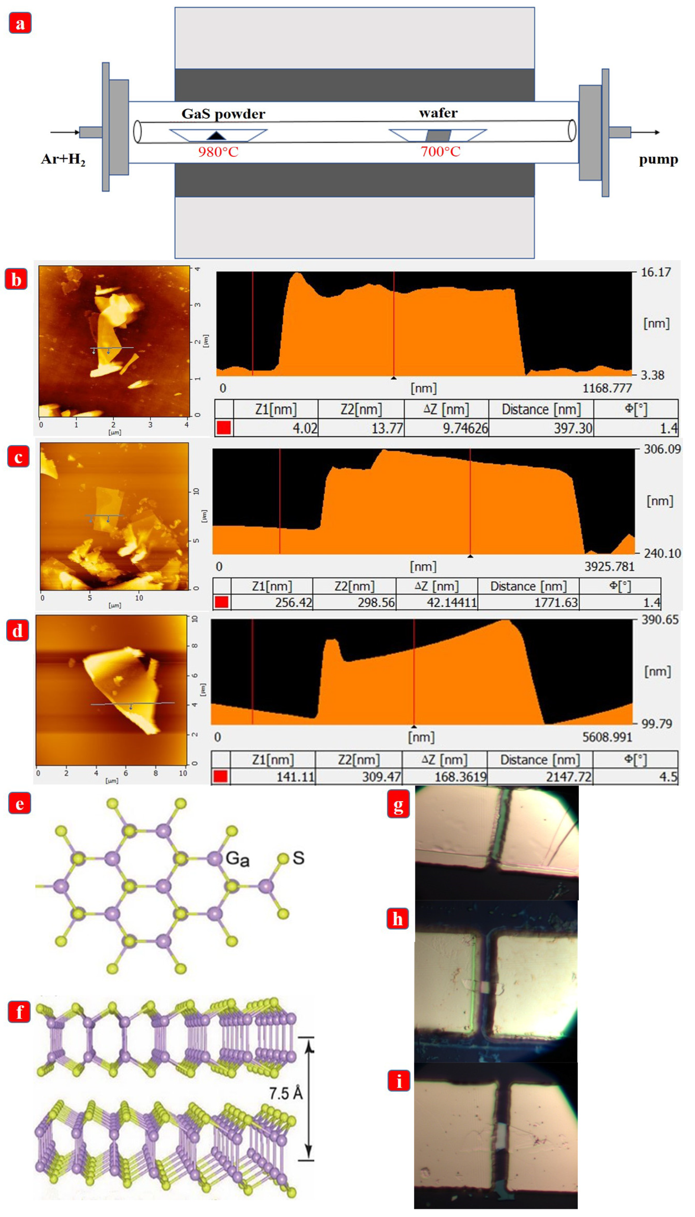
2. Experimental Sections—Preparation of Gas Nanosheets

High-quality GaS nanosheets were synthesized through CVD, using high-purity GaS powder with a purity level of 99.999%. Subsequently, these nanosheets were deposited onto a SiO2 substrate, which was characterized by an oxide layer thickness of 300 nm. Initially, a tube boiler operating at high temperatures was preheated for 2 h to establish a state of stability in the two distinct temperature zones. Then, a quartz tube was used to house a porcelain boat holding GaS powder, while another porcelain boat with a silicon substrate was positioned around 20 cm apart from the powder, as mentioned above. Next, a gas mixture comprising 100 sccm of argon and 25 sccm of hydrogen was introduced into the system. To prevent the oxidation of GaS, the reaction was conducted in a high vacuum for 2 h. The temperatures in the source and deposition substrate regions during the trials were recorded as 980 °C and 700 °C, respectively. Figure 1 shows a diagram of the GaS nanosheets fabricated using the CVD method.
Characterization of the thickness of the GaS nanosheets was performed using AFM. The lasers employed during the Raman tests had 532 and 633 nm wavelengths. The laser and collection optics were held in a fixed position during the polarization Raman experiments (Horiba LabRAM HR EVO). The polarization direction of the 532 and 633 nm lasers was manipulated by adjusting the angle of the half-wave sheet. While conducting Raman imaging tests, the sample stage underwent controlled displacement in both the x and y directions, whereas all experimental procedures were performed under ambient room-temperature conditions.
Figure 1a shows a diagram of the GaS nanosheets made using the CVD method. We obtained three thicknesses of GaS nanosheets: 10 nm in Figure 1b, 40 nm in Figure 1c, and 170 nm in Figure 1d. Shown are a top view and side view of the GaS crystal structure, showing the monolayer composed of S–Ga–Ga–S bonds and the Van der Waals interaction between layers; a thickness of 0.75 nm for a monolayer is also shown Figure 1e,f. The two-terminal devices, 1 in Figure 1g, 2 in Figure 1h, and 3 in Figure 1i, correspond to thicknesses of GaS nanosheets of 10 nm, 40 nm, and 170 nm, respectively.

3. Results and Discussion

To overcome these limitations, we employed thickness-dependent edge-enhanced Raman spectroscopy (TEER). TEER exploits the unique properties of materials with different thicknesses, such as 2D materials such as graphene or transition metal dichalcogenides, to improve the Raman signal at the edges of the materials. TEER has applications in materials science, biomedicine, and nanotechnology, and is increasingly being used to investigate the physical, chemical, and biological properties of nanomaterials.

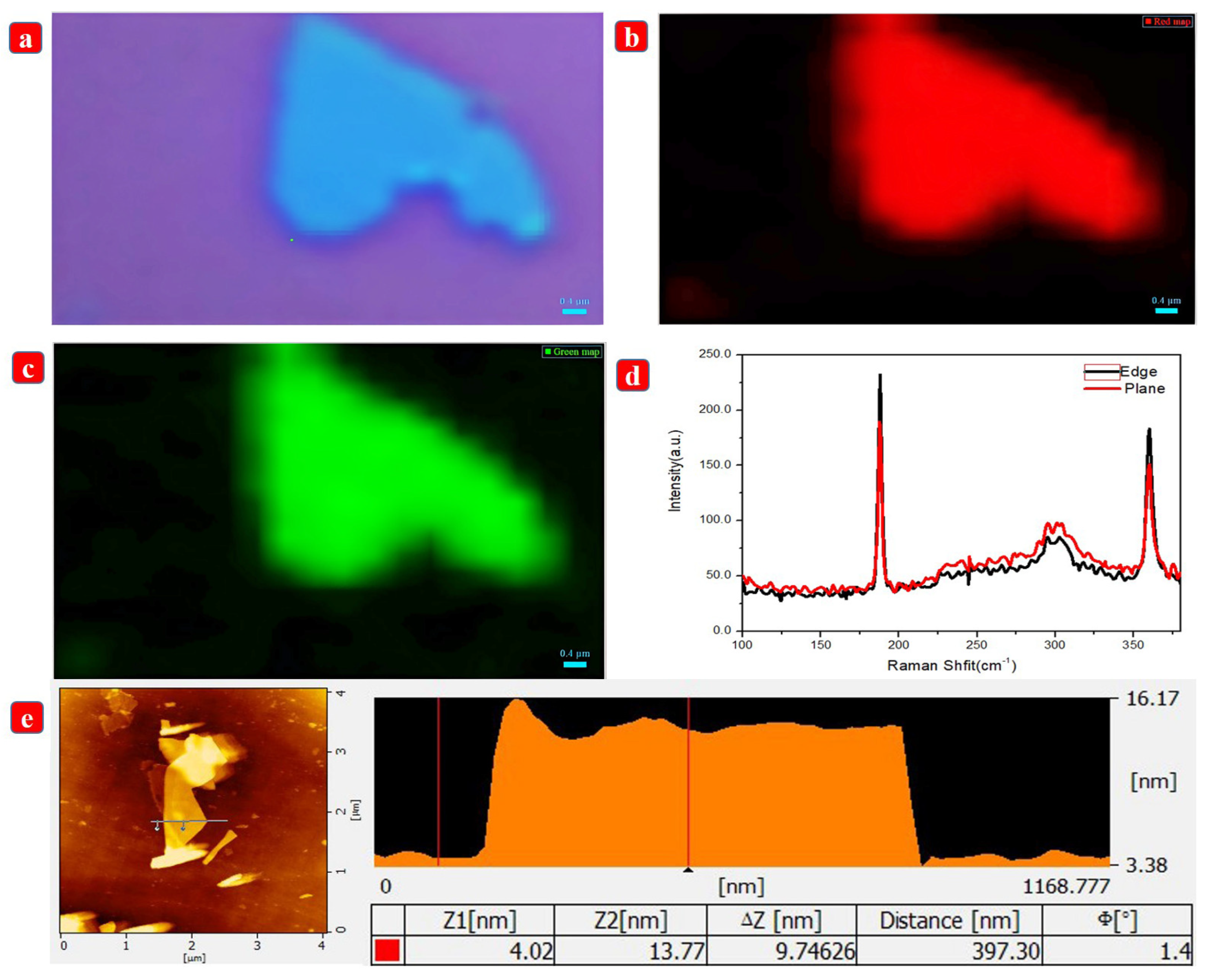
Thickness-Dependent Edge-Enhanced Raman of Gas Nanosheets

The thin GaS nanosheet depicted in Figure 2 has a thickness of approximately 10 nm, as evident from the AFM plot in Figure 2e. Figure 2a–c depict optical images, with the red and green diagrams representing the Raman peak positions at 188 and 360 cm−1, respectively. The excitation light source used for these measurements had a wavelength of 532 nm. An analysis of the Raman imaging map in Figure 2b,c reveals a uniform intensity distribution of the Raman vibration mode on the nanosheet. The intensity distribution of the Raman vibration modes on the nanosheets exhibits a homogeneous pattern. The Raman spectra depicted in Figure 2d were chosen from two distinct locations, one at the periphery and the other within the plane of the Raman imaging map. The intensities of these spectra are similar. The findings presented in this study align with those reported in previous research on GaS flakes with fewer layers [14,15,16,17].
The GaS nanosheets depicted in Figure 3 exhibit significantly greater thicknesses than those depicted in Figure 2. The thickness of these nanosheets is approximately 40 nm, as shown in the AFM image in the panel of Figure 3e. Figure 3a shows an optical image, and Figure 3b,c show Raman images at the Raman peak positions of 188 and 360 cm−1, respectively. The excitation source used had a wavelength of 532 nm. From the Raman imaging in Figure 3b,c, it can be seen that the intensity distribution of the Raman vibrational modes at the edge of the nanosheet is more pronounced than that at its plane. The provided image illustrates the Raman spectra obtained from the periphery of the Raman imaging map and any arbitrary location within the plane. The data show that the strength of the Raman vibration at the edges of the GaS nanosheets was marginally higher than that within the plane, being almost twice as much. Thus, the observed variation in the intensity distribution during Raman imaging of GaS nanosheets can be attributed to variations in their thicknesses. The electron-leaping probability of thick GaS nanosheets was enhanced because of the alteration in the lattice orientation at their edges, resulting in excellent Raman vibrational modes at these edges [18,39,40,41]. To validate this hypothesis, we used thicker GaS nanosheets for Raman analysis, while also using a 532 nm excitation light source, which generated excitement.
As shown in Figure 4a and the corresponding AFM image in Figure 4e, the GaS nanosheets exhibited a thickness of approximately 170 nm. Figure 4a shows an optical image, and the red and green figures in Figure 4b depict the Raman imaging images corresponding to Raman peaks at 188 and 360 cm−1, respectively. According to the Raman imaging figures in Figure 4b,c, the Raman vibrations at the periphery of the GaS nanosheets exhibited considerably greater intensity than those within the plane. The strength of the force in the three-dimensional space was significantly greater than that in the 2D plane. Figure 4d shows the Raman spectra obtained at the periphery of the Raman imaging map and any arbitrary location within the plane. The strength of the Raman vibration observed at the boundary of the GaS nanosheets is approximately tenfold greater than that observed within the plane. In the experiment, multiple Raman characterizations were performed on GaS samples of varying thicknesses. These results are consistent with those reported in reference [4]. The findings indicate that the thickness of GaS nanosheets is directly responsible for the observed enhancement in Raman scattering, specifically near the edges.
In Figure 2d through Figure 4d, two GaS samples with two modes, A 1 1 g and A 2 1 g , could detected at 188 and 360 cm−1, respectively. As the layer thickness drops, the intensity of the strength of the two A 1 g modes diminished dramatically. The softening of the A 1 g modes in layered materials with a decreasing number of layers was previously reported. This was observed, for example, in MoS 2 and WS 2 samples [65,66]. This effect is attributed to reducing the impact of interlayer interactions on phonon restoring forces. As the thickness of the sample decreases, surface effects have an increasing impact on the physical processes occurring in the sample. At the same time, the quality of the sample surface or effects at the sample-substrate interface may lead to the dispersion of the measured physical parameters.The behavior of the A 1 g modes with sample thickness reduction is consistent with the DFT calculations made by Rahaman et al. for a similar crystal structure of GaSe [67]. The interaction of a GaS layer with the substrate and the surface quality of the GaS layer appear to be essential elements determining the frequency values of the A 2 1 g mode of extremely thin samples and may also be responsible for the dispersion of the A 2 1 g peak locations. Furthermore, the Raman peak of a silicon substrate at 303 cm 1 influences the accuracy of the A 2 1 g mode position estimation [34,41].

4. Polarization Raman of GaS Nanosheets

To overcome these limitations, polarization Raman spectroscopy has emerged as a promising approach. By controlling the polarization of the incident and scattered light, polarization Raman spectroscopy can significantly improve the sensitivity and resolution of Raman signals. This technique exploits the anisotropic nature of molecular vibrations, allowing for more accurate detection and characterization of a sample. In addition to high-sensitivity detection, polarization Raman spectroscopy offers valuable structural information about a sample.
To advance our understanding of the correlation between the non-uniformity shown in the Raman image and the energy of laser-excited photons, as well as the polarization direction of the laser light source, we performed polarized Raman analysis of nanosheets of varying thicknesses. The nanosheets were subjected to Raman characterization using lasers with 532 and 633 nm wavelengths. The polarization direction of the incident laser light was altered in our study by adjusting the angle of the half-wave sheet. This study established the reference point for the 0 scale line on the half-wave plate as the 0 angle of the laser polarization direction. We then manipulate the half-wave plate by rotating it to achieve the desired polarization of light.
During the tests, we observed that the polarization direction of the laser only affected the intensity of the Raman vibrational modes of GaS nanosheets of a thickness of approximately 10 nm. This observation is supported by the Raman imaging plots in Figure 5b–f, as well as the Raman spectra plots in Figure 5d,g. A 532 nm laser was employed as the Raman excitation light source. Analysis of the plots in Figure 5b,c reveals that the intensity distribution of the Raman imaging maps exhibited a uniform pattern when the laser polarization direction was set at 0 . Furthermore, examination of the Raman spectra obtained from the edges of the nanosheets and any arbitrary point within the plane, as depicted in the plot in Figure 5d, demonstrates that their intensity distributions are comparable. This finding aligns with the outcomes presented in Figure 2. When the half-wave sheet was rotated at an angle of 45 , the laser light incident on the sample changed 90 relative to the 0 direction. At this point, we observed that the Raman vibrational intensity distribution remained homogeneous. However, the overall Raman intensity exhibited a slight decrease compared with that in the 0 direction, as depicted in Figure 5e–g.
The preceding findings indicate a notable amplification of Raman vibrations at the edges, as the nanosheet thickness was approximately 40 nm. Notably, nanosheets with multiple edges, such as those depicted in Figure 6a, exhibited a clear correlation between the polarization direction, excitation wavelength, and the Raman intensities at their edges. The Raman scattering for the 532 nm laser had its highest power toward the periphery, which is consistent with the observations depicted in Figure 3 and Figure 4. Nevertheless, the intensity of Raman scattering exhibited notable variations near the boundaries for specific polarization angles. The Raman imaging plots in Figure 6b,c show that the edges exhibited alternating enhancements at laser polarization angles of 0 , 60 , 90 , and 120 . This observation suggests that the enhanced Raman scattering at the edges depends on the polarization direction of the laser. Specifically, certain edges on the nanosheets exhibited significantly stronger Raman scattering in a given polarization direction compared with the other edges.
Furthermore, note that the observed phenomena of edge-enhanced Raman scattering were intricately linked to the energy of the excitation photon, explicitly referring to the wavelength of the laser employed. The Raman scattering images in Figure 6e–g show that when a 633 nm laser was used, the Raman scattering images of GaS nanosheets did not exhibit phenomena comparable to those observed when excited by a 532 nm laser at 633 nm. The Raman scattering at the edges did not have a significant enhancement effect, even when the laser polarization direction was set at 0 . The edges were significantly improved.
Therefore, apart from the above-mentioned influence of GaS nanosheet thickness, the enhancement of Raman scattering at the edges was associated with the energy of the incident photon and the polarization direction of the photon. When the nanosheet thickness was approximately 170 nm and the excitation light source was 633 nm, there was an overall reduction in the Raman scattering intensity, as seen in the GaS nanosheets. The Raman scattering images in Figure 7b,c and the Raman spectra in Figure 7d demonstrate that thicker GaS nanosheets exhibited noticeable distinctions in the polarized Raman images at the margins when subjected to 532 nm laser light. Nevertheless, note that the disparity in polarized Raman intensity between the border and surface was not substantial, particularly in the scenario where the excitation light had a wavelength of 633 nm and the angle of incidence was 0 .
These findings confirm that the Raman scattering observed in few-layer GaS nanosheets and the edge-enhancing effect observed in their polarized Raman spectra were dependent on both the thickness of the nanosheets and the energy of the incident photons used for excitation. The observed behavior could be attributed to the structural characteristics of the crystal edges, which entailed intricate interactions between electrons and photons, as well as electrons and phonons. Apart from the edge-enhanced Raman scattering identified in the samples investigated in this study, there have been previous reports regarding the aberrant behavior observed at the boundaries of 2D layered materials. The authors observed an enhancement in photoluminescence (PL) around the margins of triangular monolayer WS 2 nanosheets, as depicted in the PL photos provided (reference [37]). Various edge passivation procedures can induce alterations in the spin state of the edges of certain transition metal sulfide compounds, thereby leading to modifications in their magnetic properties at the edges [13]. Furthermore, it has been observed that an increased level of catalytic activity specifically occurs in the periphery of MoS 2 nanoparticle populations [42,43,44]. These specific events indicate that the boundaries of 2D materials significantly influence their local physicochemical properties.

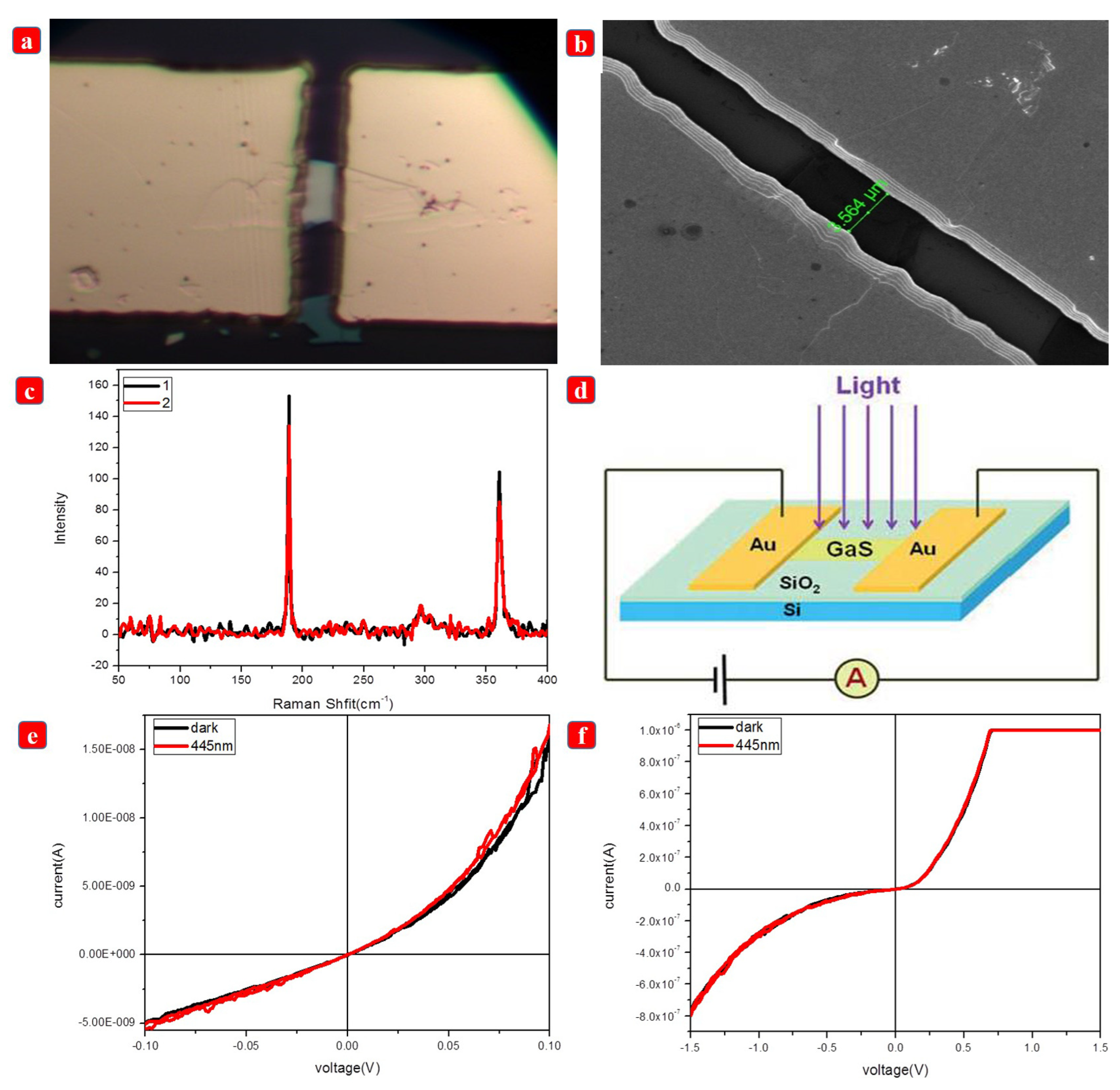
5. Optoelectronic Properties of GaS Nanosheet Devices with Different Thicknesses

Nano-solid-state devices (NSSDs) have emerged as a promising field in nanotechnology, due to their unique electronic properties and potential applications in various fields. These devices are composed of thin sheets of gas molecules, typically only a few atomic layers thick, which exhibit remarkable electronic behavior. The electronic properties of NSSDs differ significantly from those of conventional solid-state devices, making them a subject of great interest for researchers in the field.
Figure 8 shows an optical diagram of GaS two-terminal device 1, with Figure 8a showing the specific configuration. The thickness of the GaS nanosheets was approximately 170 nm. We conducted Raman imaging on the nanosheets positioned between the gold electrodes using a 532 nm laser. Based on the data shown in Figure 8b, the channel width of the device was approximately 2.1 μm. Figure 8d shows a schematic of the test device used in our study. The laser used for measuring the photocurrent had a wavelength of 455 nm. Based on the test results obtained, as shown in Figure 8e plot of I-T, the photosensitivity of the sample was highly favorable. However, note that the corresponding photocurrent was not significant. The image in Figure 8f illustrates the relationship between the photocurrent of the device and the laser power at two specific levels: 300 and 695 mW. The figure shows that there was a substantial rise in the photocurrent as the laser power increased.
Figure 9a shows an optical diagram of device 2. The thickness of the GaS nanosheets in device 2 was approximately 40 nm, as evidenced by the intensity of their Raman spectral peaks in the Raman uniform imaging plots in Figure 9c. The provided graphic illustrates that the approximate width of device 2 in Figure 9b was 3.4 μm. Figure 9d shows a graphical representation of the experiment apparatus. In the image in Figure 9e, the bottom line represents the dark current in a dark-field configuration with an applied voltage of 0.1 V. Conversely, the higher line corresponds to the photocurrent obtained when measuring the response to a 445 nm laser with a laser power of 0.695 W. The graphic illustrates the marginal rise in the current of the device upon lighting compared with the dark current. When the applied voltage was increased to 3 V under identical conditions, there was no notable alteration in the draft after lighting. This is evident when comparing the I-V plots of the dark-field current and the current during illumination, as depicted in Figure 9f.
To provide a more comprehensive examination of the effect of GaS nanosheet thickness on photocurrent, we selected the thickness of the GaS nanosheets in device 3 to be approximately 10 nm. As depicted in Figure 10a, the width of device 3 in Figure 10b was estimated to be approximately 3.5 μm. The Raman spectra in Figure 10c reveal that the Raman intensity of the sample above was lower than that of device 2. Figure 10d shows a graphical depiction of the experimental setup. Consequently, it can be inferred that the sample was a nanosheet with a reduced thickness. The dark current and photocurrent of the device were evaluated under identical conditions. The results indicated that the device exhibited limited photosensitivity. However, analysis of the I-V diagram revealed a higher dark-field current, as shown in Figure 10e, reaching a magnitude of 800 nA at an applied voltage of 1.5 V, as shown in Figure 10f. This observation suggests that the thinner GaS nanosheets possessed superior conductivity to their thicker counterparts.

6. Conclusions

In this study, we present our findings on the relationship between the thickness of few-layer GaS nanosheets and Raman scattering, as well as the polarization properties of Raman scattering. The Raman scattering intensity increased at the edges of these nanosheets as their thickness increased. Furthermore, the energy and polarization of excitation light photons significantly influenced the edge-enhanced Raman characteristics. The feature above exhibited greater prominence when nanosheets of equivalent thickness were subjected to 532 nm laser excitation instead of 633 nm laser excitation. This characterization offers a novel viewpoint on the Raman characteristics of GaS nanosheets with few layers. This is anticipated to catalyze future investigations into the possible uses of GaS and other transition metal sulfides.
In brief, the photosensitivity and conductivity of GaS nanosheet devices are significantly influenced by the thickness of GaS nanosheets. This study demonstrated the phenomenon described above through experiments conducted on GaS nanosheet devices of varying thicknesses. Specifically, three devices with different thicknesses were selected for analysis. Their values surpassed the performance of specific devices using other 2D materials. These findings could catalyze future explorations of the potential applications of GaS nanosheet-based photodetectors.

Author Contributions

Conceptualization, L.L. and Y.Z.; methodology, L.L.; validation, F.F.; formal analysis, Z.L.; investigation, Y.Z.; data curation, Z.L. and F.F.; writing-original draft preparation, Z.L., L.L. and F.F.; writing-review and editing, Y.Z. and F.Z.; project administration, Y.Z. and F.Z.; funding acquisition, F.Z. and Y.Z. All authors have read and agreed to the published version of the manuscript.

Funding

This work was supported by the National Natural Science Foundation of China (Grant No. 22175062, 21671064), the Open Project Funding of Key Laboratory of Low Dimensional Quantum Structures and Quantum Control (Grant No. QSQC2205), the Natural Science Foundation of Hunan Province of China (Grant No. 2020JJ5446, 2021JJ30232), the Scientific Research Fund of Hunan Provincial Education Department (Grant No. 19B448, 19B183), and the High-level-talent Initiation Research Fund of Hunan Police Academy (Grant No. 2021KYQD16).

Institutional Review Board Statement

Not applicable.

Informed Consent Statement

Not applicable.

Data Availability Statement

Not applicable.

Conflicts of Interest

The authors declare no conflict of interest.

References

  1. Coleman, J.N.; Lotya, M.; öNeill, A.; Bergin, S.D.; King, P.J.; Khan, U.; Young, K.; Gaucher, A.; De, H.; Smith, R.J.; et al. Two-dimensional nanosheets produced by liquid exfoliation of layered materials. Science 2011, 331, 568–571. [Google Scholar] [CrossRef]
  2. Shen, G.; Chen, D.; Chen, P.C.; Zhou, C.W. Vapor-solid growth of one-dimensional layer-structured gallium sulfide nanostructures. ACS Nano 2009, 3, 1115–1120. [Google Scholar] [CrossRef]
  3. Gutiérrez, H.R.; Perea-López, N.; Elías, A.L.; Berkdemir, A.; Wang, B.; Lv, R.; Lxoxpez-Urĺas, F.; Crespi, V.H.; Terrones, H.; Terrones, M. Extraordinary room-temperature photoluminescence in triangular WS2 monolayers. Nano Lett. 2013, 13, 3447–3454. [Google Scholar] [CrossRef] [PubMed]
  4. Méndez, B.A.R.; Lopez-Urias, F.; Terrones, M.; Terrones, H. Metallic and ferromagnetic edges in molybdenum disulfide nanoribbons. Nanotechnology 2009, 20, 325703. [Google Scholar] [CrossRef] [PubMed]
  5. Rao, C.N.R.; Sood, A.K.; Subrahmanyam, K.S.; Govindaraj, A. Graphene: The new two-dimensional nanomaterial. Angew. Chem. Int. Ed. 2009, 48, 7752–7777. [Google Scholar] [CrossRef] [PubMed]
  6. Zhang, S.; Bai, B.; Liu, J.; Zhang, J.T. Atomically dispersed catalytic sites: A new frontier for cocatalyst/photocatalyst composites toward sustainable fuel and chemical production. Catalysts 2021, 11, 1168. [Google Scholar] [CrossRef]
  7. Karvonen, L.; Säynätjoki, A.; Mehravar, S.; Rodriguez, R.D.; Hartmann, S.; Zahn, D.R.; Honkanen, S.; Norwood, R.A.; Peyghambarian, N.; Kieu, K.; et al. Investigation of second-and third-harmonic generation in few-layer gallium selenide by multiphoton microscopy. Sci. Rep. 2015, 5, 10334. [Google Scholar] [CrossRef]
  8. Cui, Y.; Peng, L.; Sun, L.; Qian, Q.; Huang, Y. Two-dimensional few-layer group-III metal monochalcogenides as effective photocatalysts for overall water splitting in the visible range. J. Mater. Chem. A 2018, 6, 22768–22777. [Google Scholar] [CrossRef]
  9. Zhuang, H.L.; Hennig, R.G. Single-Layer group-III monochalcogenide photocatalysts for water splitting. Chem. Mater. 2013, 25, 3232–3238. [Google Scholar] [CrossRef]
  10. Hu, P.; Wen, Z.; Wang, L.; Tan, P.; Xiao, K. Synthesis of few-layer GaSe nanosheets for high performance photodetectors. ACS Nano 2012, 6, 5988–5994. [Google Scholar] [CrossRef]
  11. Buscema, M.; Island, J.O.; Groenendijk, D.J.; Blanter, S.I.; Steele, G.A.; van der Zant, H.S.J.; Castellanos-Gomez, A. Photocurrent generation with two-dimensional van der Waals semiconductors. Chem. Soc. Rev. 2015, 44, 3691–3718. [Google Scholar] [CrossRef] [PubMed]
  12. Brebner, J.L. The optical absorption edge in layer structures. J. Phys. Chem. Solids 1964, 25, 1427–1433. [Google Scholar] [CrossRef]
  13. Aulich, E.; Brebner, J.L.; Mooser, E. Indirect energy gap in GaSe and GaS. Phys. Status Solidi 1969, 31, 129–131. [Google Scholar] [CrossRef]
  14. Cingolani, A.; Minafra, A.; Tantalo, P.; Paorici, C. Edge emission in GaSe and GaS. Phys. Status Solidi 1971, 4, K83–K85. [Google Scholar] [CrossRef]
  15. Adachi, S.; Hamaguchi, C. Resonant Brillouin Scattering in GaSe and GaS. J. Phys. Soc. Japan 1980, 48, 1981–1989. [Google Scholar] [CrossRef]
  16. Ho, C.H.; Lin, S.L. Optical properties of the interband transitions of layered gallium sulfide. J. Appl. Phys. 2006, 100, 083508. [Google Scholar] [CrossRef]
  17. Tverjanovich, A.; Khomenko, M.; Bereznev, S.; Fontanari, D.; Sokolov, A.; Usuki, T.; Ohara, K.; Le Coq, D.; Masselin, P.; Bychkov, E. Glassy GaS: Transparent and unusually rigid thin films for visible to mid-IR memory applications. Phys. Chem. Chem. Phys. 2020, 22, 25560–25573. [Google Scholar] [CrossRef]
  18. Carey, B.J.; Ou, J.Z.; Clark, R.M.; Berean, K.J.; Zavabeti, A.; Chesman, A.S.R.; Russo, S.P.; Lau, D.W.M.; Xu, Z.Q.; Bao, Q.; et al. Wafer-scale two-dimensional semiconductors from printed oxide skin of liquid metals. Nat. Commun. 2017, 8, 14482. [Google Scholar] [CrossRef]
  19. Jung, C.S.; Shojaei, F.; Park, K.; Oh, J.Y.; Im, H.S.; Jang, D.M.; Park, J.; Kang, H.S. Red-to-Ultraviolet emission tuning of two-dimensional gallium sulfide/selenide. ACS Nano 2015, 9, 9585–9593. [Google Scholar] [CrossRef]
  20. Harvey, A.; Backes, C.; Gholamvand, Z.; Hanlon, D.; McAteer, D.; Nerl, H.C.; McGuire, E.; Seral-Ascaso, A.; Ramasse, Q.M.; McEvoy, N.; et al. Preparation of gallium sulfide nanosheets by liquid exfoliation and their application as hydrogen evolution catalysts. Chem. Mater. 2015, 27, 3483–3493. [Google Scholar] [CrossRef]
  21. Zhang, C.; Park, S.-H.; Ronan, O.; Harvey, A.; Seral-Ascaso, A.; Lin, Z.; McEvoy, N.; Boland, C.S.; Berner, N.C.; Duesberg, G.S.; et al. Enabling flexible heterostructures for Li-Ion battery anodes based on nanotube and liquid-phase exfoliated 2D gallium chalcogenide nanosheet colloidal solutions. Small 2017, 13, 1701677. [Google Scholar] [CrossRef] [PubMed]
  22. Kato, K.; Umemura, N. Sellmeier equations for GaS and GaSe and their applications to the nonlinear optics in GaSxSe1−x. Opt. Lett. 2011, 36, 746–747. [Google Scholar] [CrossRef] [PubMed]
  23. Opoku, F.; Akoto, O.; Asare-Donkor, N.K.; Adimado, A.A. Defect-engineered two-dimensional layered gallium sulphide molecular gas sensors with ultrahigh selectivity and sensitivity. Appl. Surf. Sci. 2021, 562, 150188. [Google Scholar] [CrossRef]
  24. Cao, Y.; Cai, K.; Hu, P.; Zhao, L.; Yan, T.; Luo, W.; Zhang, X.; Wu, X.; Wang, K.; Zheng, H. Strong enhancement of photoresponsivity with shrinking the electrodes spacing in few layer GaSe photodetectors. Sci. Rep. 2015, 5, 8130. [Google Scholar] [CrossRef]
  25. Lu, Y.; Chen, J.; Chen, T.; Shu, Y.; Chang, R.J.; Sheng, Y.; Shautsova, V.; Mkhize, N.; Holdway, P.; Bhaskaran, H.; et al. Controlling defects in continuous 2D GaS films for high-Performance wavelength-tunable UV-Discriminating photodetectors. Adv. Mater. 2020, 32, 1906958. [Google Scholar] [CrossRef]
  26. Hu, Z.M.; Fei, G.T.; Zhang, L.D. Synthesis and tunable emission of Ga2S3 quantum dots. Mater. Lett. 2019, 239, 17–20. [Google Scholar] [CrossRef]
  27. Hu, P.; Wang, L.; Yoon, M.; Zhang, J.; Feng, W.; Wang, X.; Wen, Z.; Idrobo, J.C.; Miyamoto, Y.; Geohegan, D.B.; et al. Highly responsive ultrathin GaS nanosheet photodetectors on rigid and flexible substrates. Nano Lett. 2013, 13, 1649–1654. [Google Scholar] [CrossRef]
  28. Gutiérrez, Y.; Juan, D.; Dicorato, S.; Santos, G.; Duwe, M.; Thiesen, P.H.; Giangregorio, M.M.; Palumbo, F.; Hingerl, K.; Cobet, C.; et al. Layered gallium sulfide optical properties from monolayer to CVD crystalline thin films. Opt. Express 2022, 30, 27609–27622. [Google Scholar] [CrossRef]
  29. Sinha, G.; Panda, S.K.; Datta, A.; Chavan, P.G.; Shinde, D.R.; More, M.A.; Patra, A. Controlled growth of well-aligned GaS nanohornlike structures and their field emission properties. ACS Appl. Mater. Interfaces 2011, 3, 2130–2135. [Google Scholar] [CrossRef]
  30. Lei, L.; Dai, J.; Dong, H.; Geng, Y.; Cao, F.; Wang, C.; Xu, R.; Pang, F.; Liu, Z.X.; Li, F.; et al. Electronic Janus lattice and kagome-like bands in coloring-triangular MoTe2 monolayers. Nat. Commun. 2023, 14, 6320. [Google Scholar] [CrossRef]
  31. Wang, H.; Yu, L.; Lee, Y.H.; Shi, Y.; Hsu, A.; Chin, M.L.; Li, L.J.; Dubey, M.; Kong, J.; Palacios, T. Integrated circuits based on bilayer MoS2 transistors. Nano Lett. 2012, 12, 4674–4680. [Google Scholar] [CrossRef]
  32. Perkins, F.K.; Friedman, A.L.; Cobas, E.; Campbell, P.M.; Jernigan, G.G.; Jonker, B.T. Chemical vapor sensing with monolayer MoS2. Nano Lett. 2013, 13, 668–673. [Google Scholar] [CrossRef]
  33. Yin, Z.; Li, H.; Li, H.; Jiang, L.; Shi, Y.; Sun, Y.; Lu, G.; Zhang, Q.; Chen, X.; Zhang, H. Single-layer MoS2 phototransistors. ACS Nano 2012, 6, 74–80. [Google Scholar] [CrossRef] [PubMed]
  34. Dicorato, S.; Gutiérrez, Y.; Giangregorio, M.M.; Palumbo, F.; Bianco, G.V.; Losurdo, M. Interplay between thickness, defects, optical properties, and photoconductivity at the centimeter scale in layered GaS. Nanomaterials 2022, 12, 465. [Google Scholar] [CrossRef]
  35. Nicolosi, V.; Chhowalla, M.; Kanatzidis, M.G.; Strano, M.S.; Coleman, J.N. Liquid exfoliation of layered materials. Science 2013, 340, 1226419. [Google Scholar] [CrossRef]
  36. Chhowalla, M.; Shin, H.S.; Eda, G.; Li, L.J.; Loh, K.P.; Zhang, H. The chemistry of two-dimensional layered transition metal dichalcogenide nanosheets. Nat. Chem. 2013, 5, 263–275. [Google Scholar] [CrossRef]
  37. Fuhrer, M.S.; Hone, J. Measurement of mobility in dual-gated MoS2 transistors. Nat. Nanotechnol. 2013, 8, 146–147. [Google Scholar] [CrossRef] [PubMed]
  38. Novoselov, K.S.; Geim, A.K.; Morozov, S.V.; Jiang, D.; Zhang, Y.; Dubonos, S.V.; Grigorieva, I.V.; Firsov, A.A. Electric field effect in atomically thin carbon films. Science 2004, 306, 666–669. [Google Scholar] [CrossRef]
  39. Jaramillo, T.F.; Jϕrgensen, K.P.; Bonde, J.; Nielsen, J.H.; Horch, S.; Chorkendorff, I. Identification of active edge sites for electrochemical H2 evolution from MoS2 nanocatalysts. Science 2007, 317, 100–102. [Google Scholar] [CrossRef]
  40. Geim, A.K. Graphene: Status and prospects. Science 2009, 324, 1530–1534. [Google Scholar] [CrossRef]
  41. Jastrzebski, C.; Olkowska, K.; Jastrzebski, D.J.; Wierzbicki, M.; Gebicki, W.; Podsiadlo, S. Raman scattering studies on very thin layers of gallium sulfide (GaS) as a function of sample thickness and temperature. J. Phys. Condens. Matter 2019, 31, 075303. [Google Scholar] [CrossRef] [PubMed]
  42. Huang, X.; Zeng, Z.; Zhang, H. Metal dichalcogenide nanosheets: Preparation, properties and applications. Chem. Soc. Rev. 2013, 42, 1934–1946. [Google Scholar] [CrossRef] [PubMed]
  43. Zhao, Y.J.; Zhou, F. Synthesis, Evolution of Morphology, Transport Properties for Bi2Te3 Nanoplates. Crystals 2022, 12, 1668. [Google Scholar] [CrossRef]
  44. Zhao, Y.; Chen, X.; Shi, Z.; Zhou, F.; Xiang, S.; Song, K. Implementation of one-way quantum computing with a hybrid solid-state quantum system. Chin. J. Electron. 2017, 26, 27–34. [Google Scholar] [CrossRef]
  45. Chen, S.; Xiang, S.; Song, K.; Zhao, Y. Influence from cavity decay on entanglement evolution of three superconducting charge qubits coupled to a cavity. Chin. J. Electron. 2014, 23, 157–162. [Google Scholar]
  46. Tan, L.; Zhou, F.; Zhang, L.; Xiang, S.; Song, K.; Zhao, Y. High-fidelity hyperentangled cluster states of two-photon systems and their applications. Symmetry 2019, 11, 1079. [Google Scholar] [CrossRef]
  47. Zhang, H.J.; Liu, C.X.; Qi, X.L.; Dai, X.; Fang, Z.; Zhang, S.C. Topological insulators in Bi2Se3, Bi2Te3 and Sb2Te3 with a single Dirac cone on the surface. Nat. Phys. 2009, 5, 438–442. [Google Scholar] [CrossRef]
  48. Zhao, Y.J.; Fang, X.M.; Zhou, F.; Song, K.H. A scheme for realizing quantum information storage and retrieval from quantum memory based on nitrogenvacancy centers. Phys. Rev. A 2012, 86, 052325. [Google Scholar] [CrossRef]
  49. Yuan, T.; Zhou, F.; Chen, S.; Xiang, S.; Song, K.; Zhao, Y. Multipurpose quantum simulator based on a hybrid solid-state quantum device. Symmetry 2019, 11, 467. [Google Scholar] [CrossRef]
  50. Zhao, Y.; Mi, X.W.; Xiang, S.; Zhou, F.; Song, K. Entanglement dynamics of three superconducting charge qubits coupled to a cavity. Commun. Theor. Phys. 2011, 55, 775. [Google Scholar] [CrossRef]
  51. Zhou, F.; Zhao, Y.; Zhou, W.; Tang, D. Temperature-dependent raman scattering of large size hexagonal Bi2Se3 single-crystal nanosheets. Appl. Sci. 2018, 8, 1794. [Google Scholar] [CrossRef]
  52. Zhou, F.; Zhao, Y.; Zhou, W.; Tang, D. Temperature dependent raman of BiTe nanotubes. AIP Adv. 2018, 8, 125330. [Google Scholar] [CrossRef]
  53. Yang, S.; Li, Y.; Wang, X.; Huo, N.; Xia, J.B.; Li, S.S.; Li, J. High performance few-layer GaS photodetector and its unique photo-response in different gas environments. Nanoscale 2014, 6, 2582. [Google Scholar] [CrossRef] [PubMed]
  54. Zhong, W.; Liu, Y.; Yang, X.; Wang, C.; Xin, W.; Li, Y.; Liu, W.; Xu, H. Suspended few-layer GaS photodetector with sensitive fast response. Mater. Design 2021, 212, 110233. [Google Scholar] [CrossRef]
  55. Guo, Q.; Ford, G.M.; Hillhouse, H.W.; Agrawal, R. Sulfide nanocrystal inks for dense Cu(In1−xGax)(S1−ySey)2 absorber films and their photovoltaic performance. Nano Lett. 2009, 9, 3060–3065. [Google Scholar] [CrossRef]
  56. Bokova, M.; Paraskiva, A.; Kassem, M.; Bychkov, E. Raman spectra of MCl-Ga2S3-GeS2 (M = Na, K, Rb) glasses. Pure Appl. Chem. 2022, 94, 181–188. [Google Scholar] [CrossRef]
  57. Uematsu, T.; Tepakidareekul, M.; Hirano, T.; Torimoto, T.; Kuwabata, S. Facile high-yield synthesis of Ag-In-Ga-S quaternary quantum dots and coating with gallium sulfide shells for narrow band-edge emission. Chem. Mater. 2023, 35, 1094–1106. [Google Scholar] [CrossRef]
  58. Late, D.J.; Liu, B.; Luo, J.; Yan, A.; Ramakrishna Matte, H.S.S.; Grayson, M.; Rao, C.N.R.; Dravid, V.P. GaS and GaSe ultrathin layer transistors. Adv. Mater. 2012, 24, 3549–3554. [Google Scholar] [CrossRef]
  59. Schedinm, F.; Geim, A.K.; Morozov, S.V.; Hill, E.W.; Blacke, P.; Katsnelson, M.I.; Novoselov, K.S. Detection of individual gas molecules adsorbed on graphene. Nat. Mater. 2007, 6, 652–655. [Google Scholar] [CrossRef]
  60. Abderrahmane, A.; Senouci, K.; Hachemi, B.; Hachemi, B.; Ko, P.J. 2D gallium sulfide-Based 1D photonic crystal biosensor for glucose concentration detection. Materials 2023, 16, 4621. [Google Scholar] [CrossRef]
  61. Rai, J.; Gautam, S. Computational quantum chemical analysis of structural and electronic properties of functionalized gallium sulfide (GaS) nanoflakes. Mater. Today Proc. 2023, 16, 4621. [Google Scholar] [CrossRef]
  62. Zhao, Y.; Fang, X.M.; Zhou, F.; Song, K.H. Preparation of N-qubit GHZ state with a hybrid quantum system based on nitrogen-vacancy centers. Chin. Phys. Lett. 2013, 30, 050304. [Google Scholar] [CrossRef]
  63. Tan, G.J.; Zhao, L.D.; Shi, F.Y.; Doak, J.W.; Lo, S.H.; Sun, H.; Wolverton, C.; Dravid, V.P.; Uher, C.; Kanatzidis, M.G. High thermoelectric performance of p-type SnTe via a synergistic band engineering and nanostructuring approach. J. Am. Chem. Soc. 2014, 136, 7006–7017. [Google Scholar] [CrossRef] [PubMed]
  64. Abd-Elkader, O.H.; Abdelsalam, H.; Sakr, M.A.S.; Teleb, N.H.; Zhang, Q.F. Electronic and optical properties of finite gallium sulfide nano ribbons: A first-principles study. Crystals 2023, 13, 1215. [Google Scholar] [CrossRef]
  65. Berkdemir, A.; Gutiérrez, H.R.; Botello-Méndez, A.R.; Perea-López, N.; Elías, A.L.; Chia, C.I.; Wang, B.; Crespi, V.H.; López-Urías, F.; Charlier, J.C.; et al. Identification of individual and few layers of WS2 using Raman Spectroscopy. Sci. Rep. 2013, 3, 1755. [Google Scholar] [CrossRef]
  66. Li, H.; Zhang, Q.; Yap, C.C.R.; Tay, B.K.; Edwin, T.H.T.; Olivier, A.; Baillargeat, D. From bulk to monolayer MoS2: Evolution of Raman scattering. Adv. Funct. Mater. 2012, 22, 1385–1390. [Google Scholar] [CrossRef]
  67. Rahaman, M.; Bejani, M.; Salvan, G.; Lopez-Rivera, S.A.; Pulci, O.; Bechstedt, F.; Zahn, D.R. Vibrational properties of GaSe: A layer dependent study from experiments to theory. Semicond. Sci. Technol. 2018, 33, 125008. [Google Scholar] [CrossRef]
Figure 1. (a) Schematic of GaS nanosheets prepared using CVD. (b) The thickness of GaS nanosheets was approximately 10 nm from AFM. (c) The thickness of GaS nanosheets was about 40 nm from AFM. (d) The thickness of GaS nanosheets was roughly 170 nm from AFM. (e) Top view of the GaS nanosheet. (f) Side view of the GaS nanosheet. (g) Optical diagram of device 1, the thickness of the GaS nanosheet was 10 nm. (h) Optical diagram of device 2, the thickness of the GaS nanosheet was 40 nm. (i) Optical diagram of device 3, the thickness of the GaS nanosheet was 170 nm.
Crystals 13 01506 g001
Figure 2. (a) Optical picture of GaS nanosheets. (b) Imaging diagram of Raman peak position at 188 cm 1 under 532 nm laser excitation. (c) Imaging diagram of Raman peak position at 360 cm 1 under 532 nm laser excitation. (d) Raman spectra at the edge and any two points in the plane in Raman imaging plots in (b,c). (e) Thickness of GaS nanosheets was approximately 10 nm based on AFM.
Crystals 13 01506 g002
Figure 3. (a) Optical picture of GaS nanosheets. (b) Imaging image of Raman peak position at 188 cm 1 under 532 nm laser excitation. (c) Imaging diagram of Raman peak position at 360 cm 1 under 532 nm laser excitation. (d) Raman spectra at the edge and any two points in the plane in Raman imaging plots in (b,c). (e) Thickness of the GaS nanosheets was approximately 40 nm based on AFM.
Crystals 13 01506 g003
Figure 4. (a) Optical picture of GaS nanosheets. (b) Imaging of Raman peak position at 188 cm 1 under 532 nm laser excitation. (c) Imaging diagram of Raman peak position at 360 cm 1 under 532 nm laser excitation. (d) Raman spectra at the edge and any two points in the plane in Raman imaging plots in (b,c). (e) Thickness of GaS nanosheets was approximately 170 nm based on AFM.
Crystals 13 01506 g004
Figure 5. (a) Optical diagram of GaS nanosheets. (b) Imaging of Raman peak position at 188 cm 1 under 532 nm laser excitation, when the laser polarization direction was 0 . (c) Imaging of Raman peak position at 360 cm 1 when the laser polarization direction was 0 under 532 nm laser excitation. (d) Raman spectra at the edge and any two points in the plane in Raman imaging maps (b,c). (e) Raman peak position at 188 cm−1 under 532 nm laser excitation with 90 laser polarization. (f) Raman image at 360 cm 1 under 532 nm laser excitation with 90 laser polarization. (g) Raman spectra at the edge and any two points in the plane in Raman imaging diagrams (e,f).
Crystals 13 01506 g005
Figure 6. (a) Imaging of Raman peak position at 188 cm−1 under 532 nm laser excitation with laser polarization directions of a 1 = 0 , a 2 = 60 , a 3 = 90 , and a 4 = 120 . (b) Imaging of Raman peak position at 360 cm 1 under 532 nm laser excitation with laser polarization directions of b 1 = 0 , b 2 = 60 , b 3 = 90 , and b 4 = 120 . (c) Raman spectra of any two points in the Raman imaging maps (b,c) at the edge bright spot and in-plane dark spot, c 1 = 0 , c 2 = 60 , c 3 = 90 , and c 4 = 120 . (d) Raman peak position at 188 cm 1 under 633 nm laser excitation with laser polarization, d 1 = 0 , d 2 = 60 , d 3 = 90 and d 4 = 120 . (e) Imaging of Raman peak position at 360 cm 1 under 633 nm laser excitation with laser polarization, e 1 = 0 , e 2 = 60 , e 3 = 90 , and e 4 = 120 . (f) Raman spectra of any two points at the edge and at the plane in the Raman imaging diagrams (e,f) with laser polarization, g = 0 . (g) Optical diagram of GaS nanosheets.
Crystals 13 01506 g006
Figure 7. (a) Optical diagram of GaS nanosheets. (b) Imaging of Raman peak position at 188 cm 1 under 532 nm laser excitation with laser polarization, b 1 = 60 , b 2 = 120 . (c) Images of Raman peaks at 360 cm 1 under 532 nm laser excitation with laser polarization, c 1 = 60 , c 2 = 120 . (d) Raman spectra of any two points in the Raman imaging maps (b,c) at the edge bright spot and in-plane dark spot with laser polarization d 1 = 60 , d 2 = 120 . (e) Raman peak position at 188 cm 1 in the Raman imaging map under 633 nm laser excitation with laser polarization, e 1 = 60 , e 2 = 120 . (f) Raman peak at 360 cm 1 under 633 nm laser polarization, laser excitation, f 1 = 60 , f 2 = 120 . (g) Raman spectra of any two points in the Raman imaging diagrams (e,f) at the edge bright and in-plane dark spots with laser polarization, g 1 = 60 , g 2 = 120 .
Crystals 13 01506 g007
Figure 8. (a) Optical diagram of device 1. (b) Scanning electron microscopy (SEM) image of device 1. (c) Raman spectra of the edges and any point in the plane in the Raman imaging in (b). (d) Schematic of the device test model. (e) I-T plot of device 1 at 455 nm laser. (f) I-V plots of device 1 at laser powers of 300 and 695 mW.
Crystals 13 01506 g008
Figure 9. (a) Optical diagram of device 2. (b) SEM diagram of device 2. (c) Raman spectrogram of any two points in the Raman imaging plot in (b). (d) Schematic of the device test model. (e) Photocurrent plot of device 2 at 0.1 V applied voltage compared with its dark-field current. (f) Comparison of the photocurrent of device 2 with its dark-field current at 3 V applied voltage.
Crystals 13 01506 g009
Figure 10. (a) Optical diagram of device 3. (b) SEM image of device 3. (c) Raman spectra of any two points in (b). (d) Schematic of the device test model. (e) Comparison of photocurrent of device 3 with its dark-field current at 0.1 V applied voltage. (f) Comparison of photocurrent of device 3 with its dark-field current at 1.5 V applied voltage.
Crystals 13 01506 g010
Disclaimer/Publisher’s Note: The statements, opinions and data contained in all publications are solely those of the individual author(s) and contributor(s) and not of MDPI and/or the editor(s). MDPI and/or the editor(s) disclaim responsibility for any injury to people or property resulting from any ideas, methods, instructions or products referred to in the content.

