Article

Structural, Mechanical, and Piezoelectric Properties of Janus Bidimensional Monolayers

by
Abdulrahman Mallah
1,
Mourad Debbichi
2,
Mohamed Houcine Dhaou
3,* and
Bilel Bellakhdhar
4
1
Department of Chemistry, College of Science, Qassim University, Buraydah 51452, Almolaydah, Saudi Arabia
2
Laboratoire de la Matière Condensée et Nanosciences, Département de Physique, Faculté des Sciences de Monastir, Monastir 5019, Tunisia
3
Department of Physics, College of Science, Qassim University, Buraydah 51452, Almolaydah, Saudi Arabia
4
Jeddah College of Technology, Jeddah 17608, Saudi Arabia
*
Author to whom correspondence should be addressed.
Crystals 2023, 13(1), 126; https://doi.org/10.3390/cryst13010126
Submission received: 25 December 2022 / Revised: 3 January 2023 / Accepted: 6 January 2023 / Published: 10 January 2023

Abstract

:
In the present work, the noncentrosymmetric 2D ternary Janus monolayers Al 2 XX’(X/X’ = S, Se, Te and O), Si 2 XX’(X/X’ = P, As, Sb and Bi), and A 2 PAs(A = Ge, Sn and Pb) have been studied based on first-principles calculations. We find that all the monolayers exhibit in-plane d 12 , and out-of-plane d 13 piezoelectric coefficients due to the lack of reflection symmetry with respect to the central A atoms. Moreover, our calculations show that Al 2 OX(T = S, Se, Te) chalcogenide monolayers have higher absolute in-plane piezoelectric coefficients. However, the highest out-of-plane values are achieved in the Si 2 PBi monolayer, larger than those of some advanced piezoelectric materials, making them very promising transducer materials for lightweight and high-performance piezoelectric nanodevices.

1. Introduction

During the last 10 years, the study of two-dimensional (2D) materials has received a lot of attention as a result of the successful exfoliation of a graphene monolayer and the revealing of its special properties [1,2,3]. This class of materials can have significantly different, and sometimes unexpected properties compared to their bulk counterparts [4,5].
Among these, the Janus materials, which are characterized by two faces with two different local environment, have received rapidly increasing attention in recent years [6,7,8,9]. This new type of 2D material is successfully predicted by using first-principles calculations and is exfoliated mechanically from its bulk. The Janus-type two-dimensional (2D) monolayers have been studied extensively both experimentally and theoretically. They have many new physical properties that are not present in bulk structures or other conventional 2D materials. They also possess many exceptional physical properties, making them good candidates for many fields like electronics, optoelectronics, and catalysis. For instance, the potential of these stable 2D In 2 X 2 X’ (X and X’ = S, Se, and Te) for photocatalytic and piezoelectric applications have been predicted by first-principles calculations [10]. Tuan et al. have predicted by first-principles calculations a novel stable Janus group III chalcogenide monolayers Al 2 XY 2 (X/Y = S, Se, Te) suitable for applications in high-performance electronic nanodevices [8]. It has also been demonstrated by using first-principles calculations that the Janus Si 2 XY (X,Y = P, As, Sb, Bi) monolayers have the potential for applications in spintronic devices [11]. Very recently, Yungang et al. [9] demonstrated that Nb 3 SBr 7 and Ta 3 SBr 7 bilayers are promising photocatalysts for water splitting due to their experimental feasibility and their distinct characteristic such as robust coexistence of intrinsic charge separations, ultrahigh solar-to-hydrogen (STH) efficiencies, and strong absorptions.
Piezoelectricity is a particularly interesting and useful property that has attracted tremendous interest because it allows for energy conversion between electrical and mechanical energy or vice versa. The growing demands for nanoscale and diverse functional piezoelectric devices have oriented researchers to explore low-dimensional piezoelectric materials. However, the piezoelectric effect is an electromechanical interaction between stresses and strains, and polarizations and electric fields in noncentrosymmetric semiconductors and insulators [12,13,14]. It has been revealed that the lack of mirror symmetry in Janus structures has resulted in many new physical effects that are not present in symmetric structures such as the piezoelectric effect. This class of piezoelectric materials has numerous promising applications in sensors, transducers, actuators, active flexible electronics, and energy conversion devices [15,16]. As shown by Yonghu et al. [17] the coupling of topology and piezoelectricity in Janus MTeS (M = Ga and In) monolayers may offer a new platform for novel spintronic and piezotronic device applications. Additionally, the monolayer Fe 2 IX (X = Cl and Br) becomes a viable platform for multifunctional spintronic applications with a large gap and high Curie temperature, due to the combination of piezoelectricity, topology, and the ferromagnetic ordering [18]. Furthermore, the coexistence of piezoelectricity and magnetism and their interaction in 2D materials can be utilized for making piezoelectric-based multifunctional nanodevices [19,20]. Despite the existence of many works about piezoelectricity properties based on binary 2D materials, few works are down for 2D ternary. However, the search for new materials with large piezoelectric coefficients remains a challenge for nanogenerators, ultrasensitive mechanical detectors, and consumer touch-sensor applications. Here, by using the density-functional perturbation theory, we have predicted the piezoelectric coefficients of some stable Janus monolayers, including Al 2 XX’(X/X’=S, Se, Te and O), Si 2 XX’(X/X’=P, As, Sb and Bi) and A 2 PAs(A=Ge, Sn and Pb). These Janus monolayers are distinguished by the lack of mirror symmetry. We find that all the monolayers exhibit an in-plane d 12 and out-of plane d 13 piezoelectric coefficients. Our first-principles calculations show Al 2 OX(T = S, Se, Te) chalcogenide monolayers have larger absolute in-plane piezoelectric coefficients. However, the highest out-of-plane value is achieved in the Si 2 PBi monolayer, higher than those of some advanced piezoelectric materials.

2. Computational Details and Methods

Our DFT calculations are performed by using the Vienna ab initio simulation package (VASP) [21] and the projector-augmented wave method (PAW) with a cutoff energy of 600 eV. For the exchange-correlation potential, the generalized gradient approximation (GGA) within the Perdew–Burke–Ernzerhof (PBE) formalism is employed [22]. The Brillouin zone integration is sampled by using a Γ -centered 16 × 16 × 1 k-point grid. For the all Janus A 2 XX’ monolayers, a vacuum spacing higher than 20 Å along the the direction perpendicular to the plane is included to avoid interactions between two neighboring images.
Elastic stiffness was calculated, including ionic relaxations by using the finite differences method [23]. However, the piezoelectric stress coefficients were calculated by employing the density functional perturbation theory (DFPT) method [23]. For more accurate results, a dense k-point mesh 25 × 25 × 1 is used. All the structures are fully relaxed by using 10 6 eV and 10 3 eV/Å as convergence criteria for total energy and Hellmann–Feynman force, respectively. The localization of electrons in one unit cell with one monolayer is estimated by using the electron localization function (ELF) analysis, which was introduced in quantum chemistry to identify regions of space that can be associated with electron pairs [24].

3. Results and Discussion

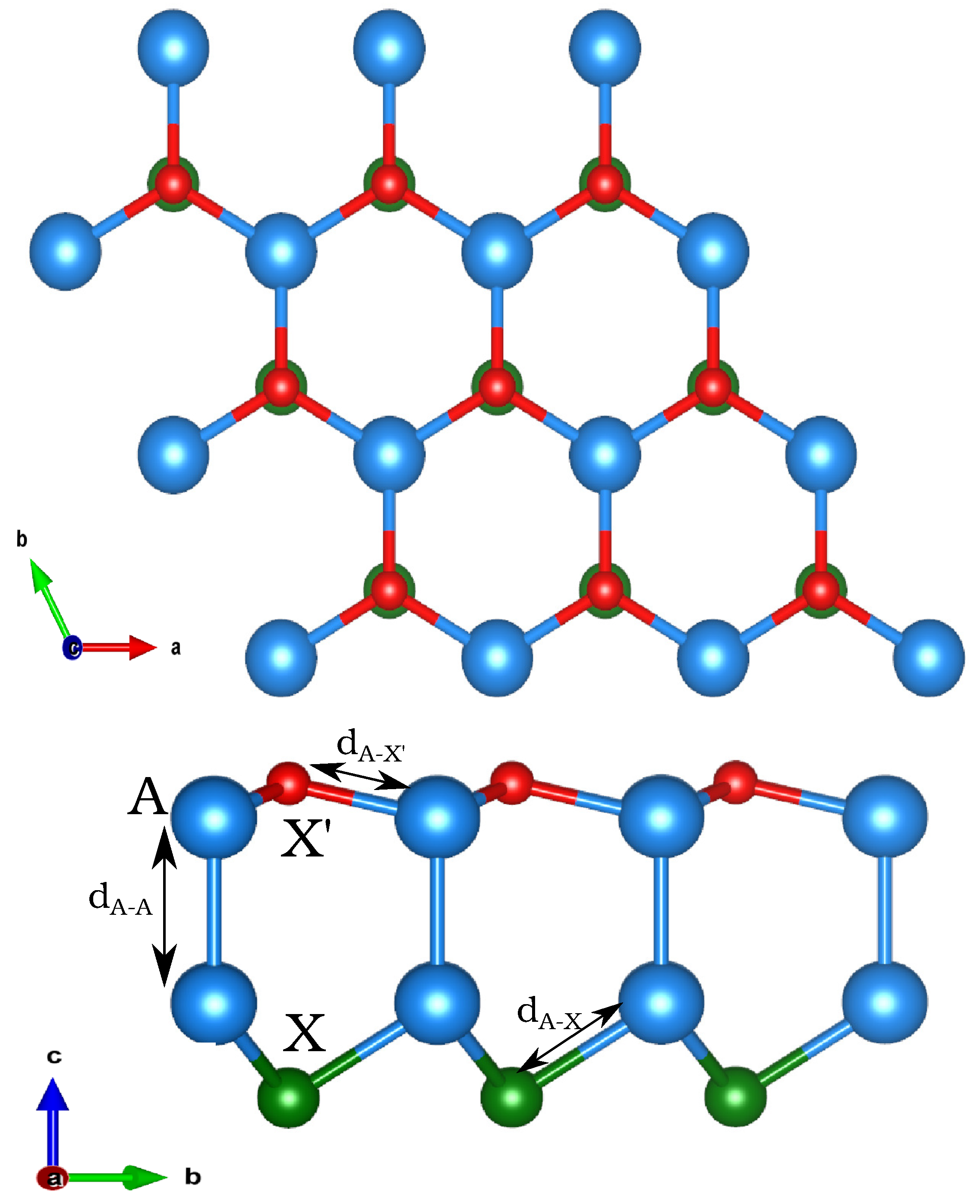
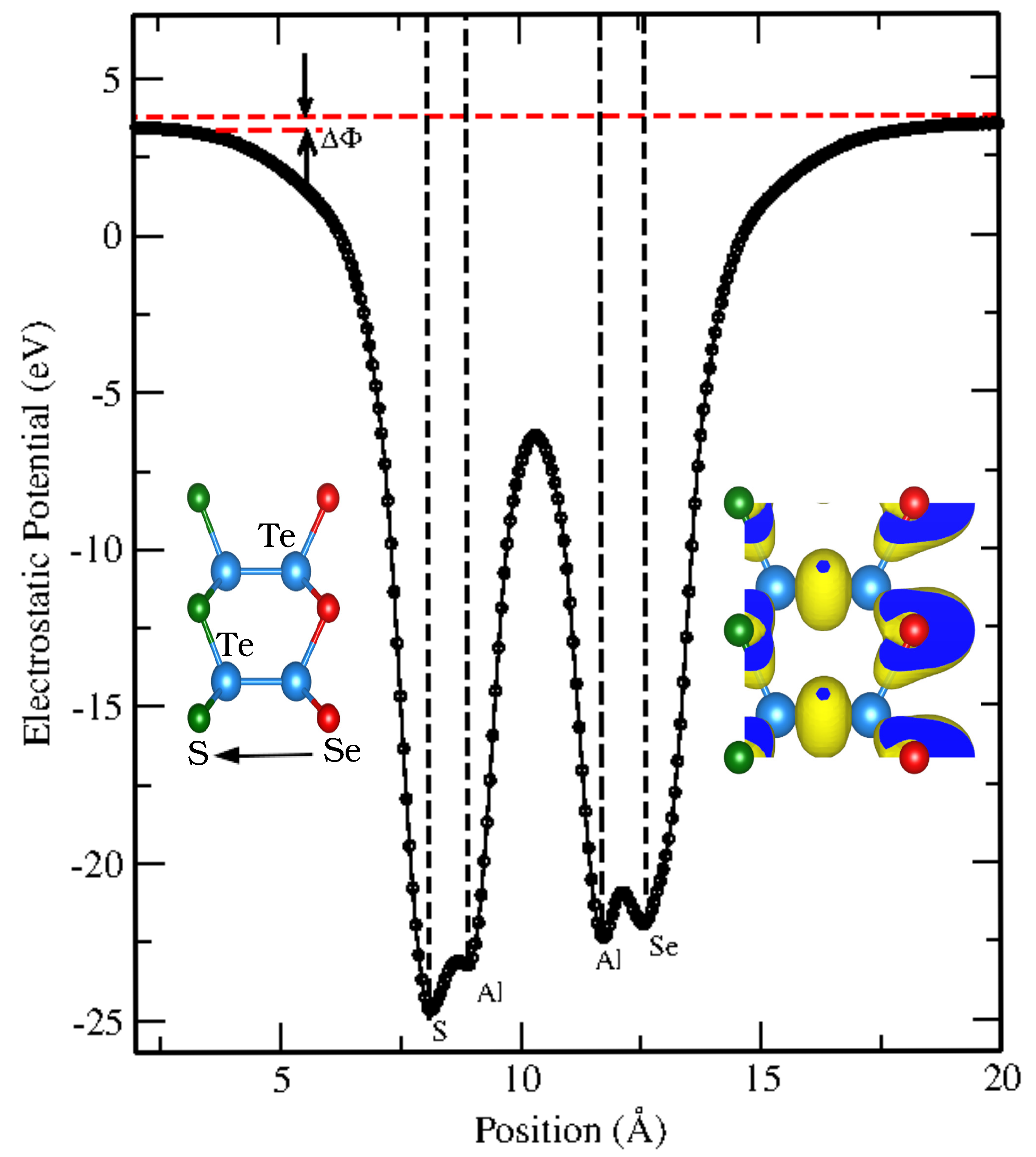
3.1. Crystal Structures and Symmetry

In this paper, 15 possible models of A 2 XX’ monolayer, including Al 2 XX’(X/X’ = S, Se, Te and O), Si 2 XX’(X/X’ = P, As, Sb and Bi) and A 2 PAs(A = Ge, Sn and Pb) are modeled. Figure 1 shows the top and side views of the optimized lattice structure of the Janus A 2 XX’ monolayers. The unit cell has a hexagonal symmetry with a C 3 v space group, and are made up of one X atom, one X’ atom, and two A atoms layers sandwiched between X and X’ atomic layers in the sequence X-A-A-X’. The absence of inversion symmetry distinguishes these monolayers from their parent binary structure.
It was proven by previous theoretical works [11,25,26,27,28] based on static energy, phonon spectrum, and ab initio molecular dynamics simulations that all the Al 2 XX’ monolayers have thermal and kinetic stability. Meanwhile, DFT calculations that use different exchange-correlation functionals, such as PBE and HSE06, have been used to report the band structures of these monolayers. The calculated structural parameters of Al 2 XX’ monolayers are listed in Table 1. The obtained results are in good agreement with the available data [11,25,26,27].

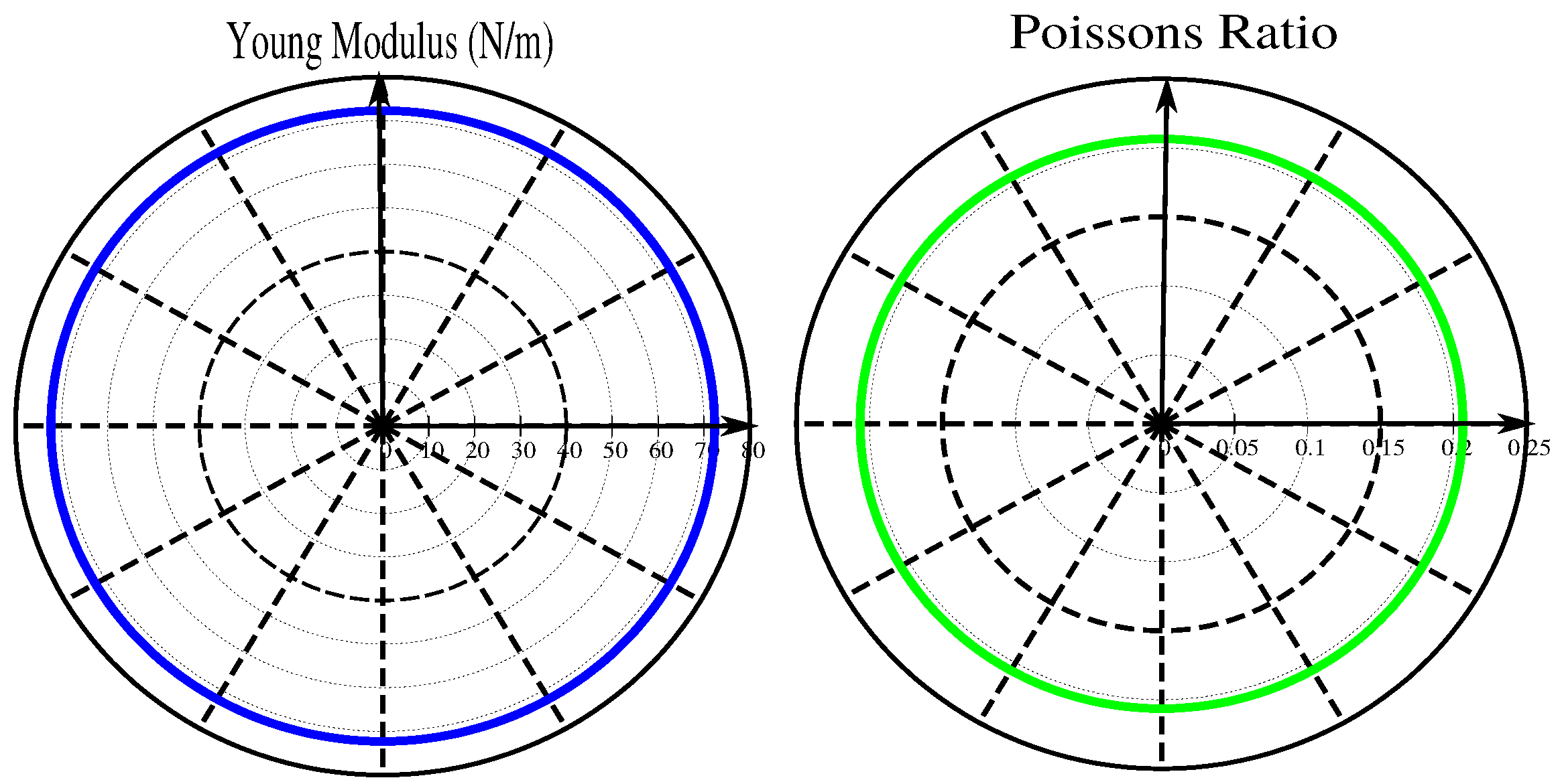
3.2. Elastic Theory and Properties

According to the symmetry group of our 2D compounds, only four elastic constants are nonzero, C 11 , C 22 , C 12 , and C 66 . Due to the symmetry of structures, we have C 11 = C 22 et C 66 = 1 2 (C 11 -C 12 ). The calculated elastic constants C i j are listed in Table 2. By checking the Born–Huang stability criteria [25]: C 11 > C 12 , C 22 > 0, C 66 > 0, and C 11 2 - C 21 2 > 0, we show that all the monolayers satisfy the stability condition.
The elastic properties of the A 2 XX’ monolayers are examined in terms of the in-plane Young modulus and the Poisson ratios. Due to hexagonal symmetry, A 2 XX’ monolayers are mechanically isotropic.
In terms of these elastic constants, the layer modulus is
γ 2 D = 1 2 ( C 11 + C 12 ) .
The angular dependence of the in-plane Poisson’s ratio ( ν 2 D ( θ ) ) and Young’s modulus (Y 2 D ( θ )) are obtained from the following formulas [1]:
ν 2 D ( θ ) = C 12 S 4 B S 2 C 2 + C 12 C 4 C 11 S 4 + A S 2 C 2 + C 22 C 4
Y 2 D ( θ ) = C 11 C 22 C 12 2 C 11 S 4 + A S 2 C 2 + C 22 C 4
where S = s i n ( θ ) , C = c o s ( θ ) , A = C 11 C 22 C 12 2 C 66 2 C 12 and B = C 11 + C 12 C 11 C 22 C 12 2 C 66 .
The orientation-dependent values for the all monolayers reveal strong isotropy of Young’s modulus as well as Poisson’s ratio. As an example, we show in Figure 2 the angular dependence of the Poisson’s ratio (a) and Young’s modulus of Al 2 SSe monolayer. We find that ν 2 D and Y 2 D plots are perfect circulars, implying that these monolayers have highly isotropic elasticity due to their 2D isotropic atomic structures. The corresponding computed values are listed in Table 2. For the all monolayers, our calculated values of the elastic stiffness are in concordance with the available data [11,25,26]. The Young’s moduli values are obviously smaller than those of other well-known 2D materials, such as graphene, hexagonal boron nitrite layer and MoS 2 [29,30,31], demonstrating their mechanical flexibility and can resist significantly to the mechanical strain. The calculated ν 2 D values of all the monolayers except Si 2 PBi are less than 0.33, which implies that these monolayers are brittle based on the Frantsevich rule [32,33].

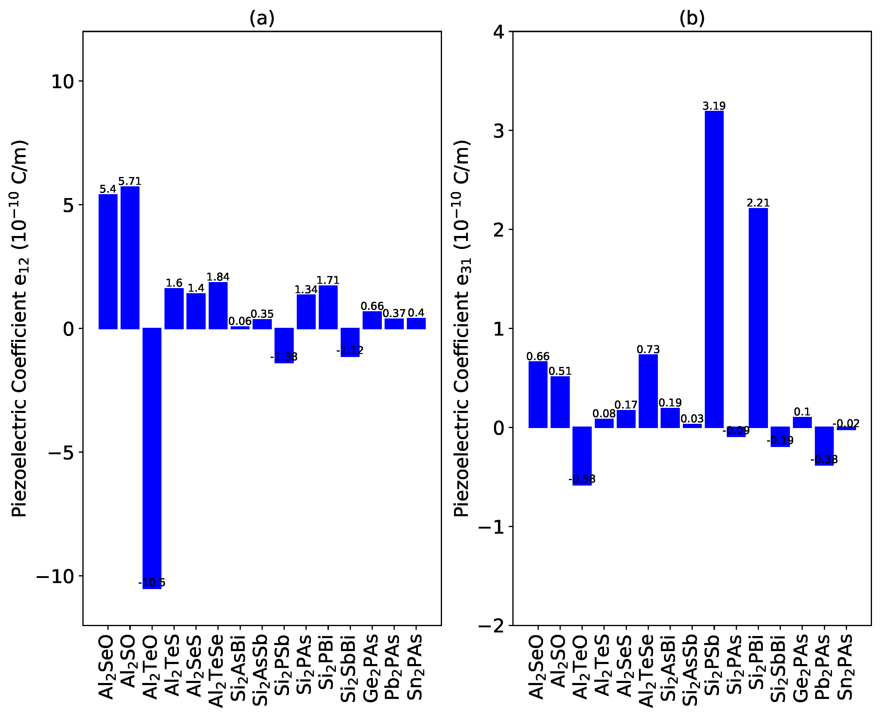
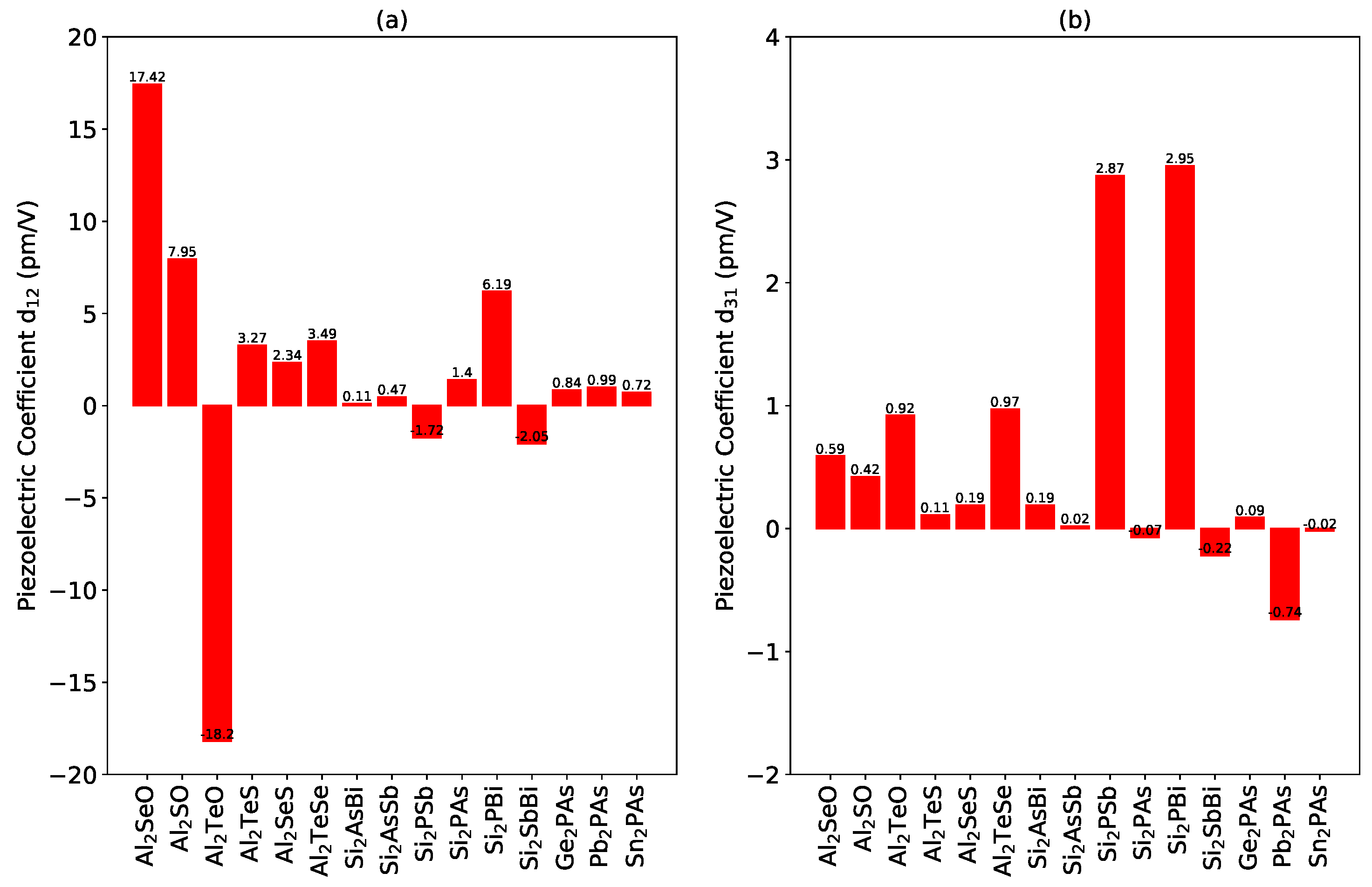
3.3. Piezoelectric Properties

In A 2 XX’, the difference in atom size and electronegativity, as well as the different bond types between Al-X (d A X ) and Al-X’(d A X ) all contribute to unequal charge distributions in the systems as shown in the inset of the Figure 3, resulting in noncentrosymmetric materials. As an example, the planar average of the electrostatic potential energy of Al 2 SSe is shown in Figure 3. As can clearly be seen, a significant potential difference between the two sides of the monolayer, reflecting the formation of an internal electric field and surface work function difference ( Δ Φ ). For the other compounds, the planar average of the electrostatic potential energy is calculated and the extracted work function difference is regrouped in Table 1, which is proportional to the magnitude of the dipole moment according to the Helmholtz equation [34].
The aforementioned properties, such as the lack of inversion symmetry and the intrinsic polar electric field, are two possible causes for the emergence of piezoelectricity in the materials. The relaxed-ion third-rank piezoelectric tensors e i j k and d i j k , which are the sum of ionic and electronic contributions, can be evaluated by
e i j k = e i j k i o n + e i j k e l c = P i ε i j
and
d i j k = d i j k i o n + d i j k e l c = P i σ i j ,
where ε i j , σ i j and P i represent the strain, stress, and polarization tensors, respectively. For 2D materials, ε i j = σ i j = 0 for i = 3 [16].
By using the Voigt notation, (1 = xx, 2 = yy, 3 = zz, 4 = yz, 5 = zx, and 6 = xy) [35]. The second-rank piezoelectric tensors e i j and d j k are related via the elastic stiffness tensor by
e i j = d i k C j k .
For our Janus monolayers the point-group symmetry belongs to 3m, and the nonzero piezoelectric stress tensors, e i j are given as
e i j = . . . . e 15 e 12 e 12 e 12 . e 15 . . e 31 e 31 e 31 . . .
For 2D materials e i j 2 D =d i k 2 D C j k , where M i j 2 D = M / l z , (M = e or d), and l z is the length of the unit cell along the z direction.
Based on Equation (6), the unique in-plane and out-of-plane piezoelectric coefficients e 12 2 D , d 12 2 D and e 31 2 D , d 31 2 D , respectively, are nonzero. The corresponding piezoelectric tensors matrix can be written as
0 0 e 12 2 D e 12 2 D e 12 2 D 0 e 31 2 D e 31 2 D 0 = 0 0 2 d 12 2 D d 12 2 D d 12 2 D 0 d 31 2 D d 31 2 D 0 × C 11 C 12 0 C 12 C 11 0 0 0 C 66 .
The d 22 and d 31 can be calculated by
d 12 2 D = e 12 2 D C 11 C 22
and
d 31 2 D = e 31 2 D C 11 + C 22 .
In the following, we use e i j and d i j instead of the e i j 2 D and d i j 2 D symbol, respectively. In this work, we adapted the relaxed-ion method, which is the sum of electronic and ionic parts to calculate the piezoelectric coefficients, which is the more reliable method compared to that of the clamped-ion one [36]. To verify the reliability of the applied method, we have first computed piezoelectric stress coefficient e 11 for 1H-MoS 2 monolayer and found a predicted value as higher as ∼2.27 × 10 10 C/m, in excellent agreement with the experimental value and the reported theoretical studies [12,37]. By using the above procedures, we derive the piezoelectric coefficients e i j of the all monolayers. The results are shown in Figure 4. More significantly, these Janus monolayers with broken mirror symmetry possess, in addition to in-plane e 12 /d 12 nonzero out-of-plane piezoelectric coefficients e 13 /d 13 . The minus sign in calculated values indicates the direction of polarization.
As shown in Figure 4a and Figure 5a for a given metal element A, the monolayers containing heavier chalcogenide atoms (Te, Se and S) have the higher in-plane piezoelectric coefficient e 12 / d 12 values. Compared with other 2D piezoelectric materials such as MoX 2 (X = S, Se, Te) and MoTO (T = S, Se, Te) with a value of 3.64–5.43 pm/V [30,38], the Janus Al 2 OX(T = S, Se, Te) chalcogenide monolayers have larger absolute in-plane piezoelectric coefficients by several folds. More noticeably, d 12 attains 18.20 and 17.42 pm/V for Al 2 TeO and Al 2 SeO monolayers, respectively, in same order of magnitude as the Janus M 2 SeX (M = Ge, Sn; X = S, Te) monolayers [13], which makes them appropriate for 2D piezoelectric sensors and nanogenerators. Some materials, such as the monolayers Al 2 TeSe and Si 2 PBi, have large d 12 values but small e 12 values because their Young’s moduli are small, limiting the amount of force applied in electric field-induced deformations.
The noncentrosymmetric crystal structure of the A 2 XX’ monolayers in the out-of-plane direction gives rise to the finite out-of-plane piezoelectric constant. For all the monolayers presented in this work, the value of the out-of-plane strain piezoelectric coefficient d 31 (Figure 5b) is about two orders of magnitude lower than the in-plane coefficient d 12 . This means that vertical piezoelectric polarization due to vertical strain is much stronger than that of the in-plane strain. But these values are still comparable to other 2D materials such as Te 2 Se, MoSTe, In 2 SSe, TiNX 0.5 Y 0.5 (X, Y = Cl, Br, F) and 1T-MX 2 (M = Zr and Hf; X = S, Se, and Te) [16,39,40]. The highest d 31 value (2.95 pm/V) is achieved in the Si 2 PBi and Si 2 PSb monolayers, higher to those of some advanced piezoelectric materials such as MoSTe, GaN wirtzite, M 2 XX’(M = Ga, In; X, X’ = S, Se, Te and X≠X’) and MM’X 2 (M, M’ = Ga, In and M’≠M; X = S, Se, Te) [16,36]. This value is also comparable to that of the Janus Te 2 Se multilayers with antiparallel orientations, CrF 1.5 I 1.5 , Sb 2 Te 2 Se, Sb 2 Se 2 Te, TePtS and TePtSe [14,16,41,42]. This significant out-of-plane piezoelectric effect would give these Janus monolayers a variety of functions in piezoelectric applications.
By comparing the d 31 of the six 2D Janus Si 2 XX’ monolayers, we conclude that the absolute value of the out-of-plane piezoelectric coefficient d 31 increases with the electronegativity difference between the atoms on both sides of the monolayer, X and X’. This finding is also valid for the Al 2 XX’ monolayers. This is understandable given that the difference in atomic sizes of X and X’ breaks the reflection symmetry along the vertical direction, resulting in vertical piezoelectric polarization, which becomes stronger when the electronegativity difference between atoms increases.

4. Conclusions

On the basis of first-principles calculations, we have systematically studied the piezoelectric properties of some Janus 2D monolayers, Al 2 XX’(X/X’ = S, Se, Te and O), Si 2 XX’(X/X’ = P, As, Sb and Bi) and A 2 PAs(A = Ge, Sn and Pb). The absence of inversion symmetry in these Janus structures gives rise to in-plane and out-of-plane piezoelectric coefficients. Our calculations, by using the DFPT method, reveal that the monolayers containing heavier chalcogenide atoms (Te, Se and S) have a higher in-plane piezoelectric coefficient larger than those of the widely studied 1H-MoX 2 (X = S, Se, Te) monolayers. Moreover, all the monolayers are characterized by out-of-plane piezoelectric coefficients e 31 /d 31 , due to the lack of reflection symmetry with respect to the central A atoms. The highest values of d 31 (∼2.9 pm/V) are achieved for the Si 2 PBi and S 2 PSb monolayers due to their mechanical flexibility.

Author Contributions

Conceptualization: A.M., M.D., M.H.D. and B.B.; Data curation: A.M., M.D. and M.H.D.; Formal analysis: M.D., M.H.D. and B.B.; Funding acquisition: A.M. and M.H.D.; Investigation: A.M. and M.D.; Resources: M.D.; Validation: A.M. and M.D.; Writing-original draft: A.M., M.D. and M.H.D. All authors have read and agreed to the published version of the manuscript.

Funding

Qassim University, represented by the Deanship of Scientific Research, on the material support for this research under the number (10244-cos-2020-1-3-I).

Data Availability Statement

Data can be requested from the authors.

Acknowledgments

The authors gratefully acknowledge Qassim University, represented by the Deanship of Scientific Research, on the material support for this research under the number (10244-cos-2020-1-3-I) during the academic year 1442AH/2020AD.

Conflicts of Interest

On behalf of all authors, the corresponding author states that there is no conflict of interest.

References

  1. Debbichi, M.; Alhodaib, A. Stability, electronic and magnetic properties of the penta-CoAsSe monolayer: A first-principles and Monte Carlo study. Phys. Chem. Chem. Phys. 2022, 24, 5680. [Google Scholar] [CrossRef] [PubMed]
  2. Debbichi, M.; Mallah, A.; Dhaou, M.H.; Lebègue, S. First-Principles Study of Monolayer penta-CoS2 as a Promising Anode Material for Li/Na-ion Batteries. Phys. Rev. Appl. 2021, 16, 024016. [Google Scholar] [CrossRef]
  3. Debbichi, M.; Said, H.; Garbouj, H.; El Hog, S.; An Dinh, V. A new ternary Pentagonal Monolayer based on Bi with large intrinsic Dzyaloshinskii-Moriya interaction. J. Phys. D Appl. Phys. 2021, 55, 015002. [Google Scholar] [CrossRef]
  4. Debbichi, M.; Debbichi, L.; Lebègue, S. Tuning the magnetic and electronic properties of monolayer chromium tritelluride through strain engineering. Phys. Lett. A 2020, 384, 126684. [Google Scholar] [CrossRef]
  5. Debbichi, M.; Debbichi, L.; Lebègue, S. Controlling the stability and the electronic structure of transition metal dichalcogenide single layer under chemical doping. Phys. Lett. A 2019, 383, 2922–2927. [Google Scholar] [CrossRef]
  6. Sa, B.; Hu, R.; Zheng, Z.; Xiong, R.; Zhang, Y.; Wen, C.; Zhou, J.; Sun, Z. High-Throughput Computational Screening and Machine Learning Modeling of Janus 2D III–VI van der Waals Heterostructures for Solar Energy Applications. Chem. Mater. 2022, 34, 6687–6701. [Google Scholar] [CrossRef]
  7. Zhang, L.; Gu, Y.; Du, A. Two-Dimensional Janus Antimony Selenium Telluride with Large Rashba Spin Splitting and High Electron Mobility. ACS Omega 2021, 6, 31919–31925. [Google Scholar] [CrossRef]
  8. Vu, T.V.; Hieu, N.N. Novel Janus group III chalcogenide monolayers Al2XY2 (X/Y = S, Se, Te): First-principles insight onto the structural, electronic, and transport properties. J. Phys. Condens. Matter 2021, 34, 115601. [Google Scholar] [CrossRef]
  9. Zhou, Y.; Zhou, L.; He, J. 2D Nb3SBr7 and Ta3SBr7: Experimentally Achievable Janus Photocatalysts with Robust Coexistence of Strong Optical Absorption, Intrinsic Charge Separation, and Ultrahigh Solar-to-Hydrogen Efficiency. ACS Appl. Mater. Interfaces 2022, 14, 1643–1651. [Google Scholar] [CrossRef]
  10. Wang, P.; Liu, H.; Zong, Y.; Wen, H.; Xia, J.B.; Wu, H.B. Two-Dimensional In2X2X’ (X and X’ = S, Se, and Te) Monolayers with an Intrinsic Electric Field for High-Performance Photocatalytic and Piezoelectric Applications. ACS Appl. Mater. Interfaces 2021, 13, 34178–34187. [Google Scholar] [CrossRef]
  11. Babaee Touski, S.; Ghobadi, N. Structural, electrical, and Rashba properties of monolayer Janus Si2XY (X,Y =P, As, Sb, and Bi). Phys. Rev. B 2021, 103, 165404. [Google Scholar] [CrossRef]
  12. Blonsky, M.N.; Zhuang, H.L.; Singh, A.K.; Hennig, R.G. Ab Initio Prediction of Piezoelectricity in Two-Dimensional Materials. ACS Nano. 2015, 9, 9885–9891. [Google Scholar] [CrossRef] [PubMed]
  13. Qiu, J.; Zhang, F.; Li, H.; Chen, X.; Zhu, B.; Guo, H.; Ding, Z.; Bao, J.; Yu, J. Giant Piezoelectricity of Janus M2SeX (M = Ge, Sn; X = S, Te) Monolayers. IEEE Electron Device Lett. 2021, 42, 561–564. [Google Scholar] [CrossRef]
  14. Guo, S.D.; Guo, X.S.; Cai, X.X.; Mu, W.Q.; Ren, W.C. Intrinsic piezoelectric ferromagnetism with large out-of-plane piezoelectric response in Janus monolayer CrBr1.5I0.5. J. Appl. Phys. 2021, 129, 214301. [Google Scholar] [CrossRef]
  15. Wu, W.; Wang, Z.L. Piezotronics and piezo-phototronics for adaptive electronics and optoelectronics). Nat. Rev. Mater. 2016, 1, 16031. [Google Scholar] [CrossRef]
  16. Chen, Y.; Liu, J.; Yu, J.; Guo, Y.; Sun, Q. Symmetry-breaking induced large piezoelectricity in Janus tellurene materials. Phys. Chem. Chem. Phys. 2019, 21, 1207–1216. [Google Scholar] [CrossRef] [PubMed]
  17. Wang, Y.; Lei, S.; Huang, Q.; Wan, N.; Xu, F.; Yu, H.; Li, C.; Chen, J. Coexistence of the Piezoelectricity and Intrinsic Quantum-Spin Hall Effect in GaTeS and InTeS Monolayers: Implications for Spintronic Devices. ACS Appl. Nano Mater. 2022, 5, 11037–11044. [Google Scholar] [CrossRef]
  18. Guo, S.D.; Mu, W.Q.; Xiao, X.B.; Liu, B.G. Intrinsic room-temperature piezoelectric quantum anomalous hall insulator in Janus monolayer Fe2IX (X = Cl and Br). Nanoscale 2021, 13, 12956–12965. [Google Scholar] [CrossRef] [PubMed]
  19. Guo, S.D.; Zhu, Y.T.; Qin, K.; Ang, Y.S. Large out-of-plane piezoelectric response in ferromagnetic monolayer NiClI. Appl. Phys. Lett. 2022, 120, 232403. [Google Scholar] [CrossRef]
  20. Noor-A-Alam, M.; Nolan, M. Large piezoelectric response in ferroelectric/multiferroelectric metal oxyhalide MOX2 (M = Ti, V and X = F, Cl and Br) monolayers. Nanoscale 2022, 14, 11676–11683. [Google Scholar] [CrossRef]
  21. Kresse, G.; Hafner, J. Ab initio molecular dynamics for liquid metals. Phys. Rev. B 1993, 47, 558–561. [Google Scholar] [CrossRef] [PubMed]
  22. Perdew, J.P.; Burke, K.; Ernzerhof, M. Generalized Gradient Approximation Made Simple. Phys. Rev. Lett. 1996, 77, 3865. [Google Scholar] [CrossRef] [PubMed] [Green Version]
  23. Wu, X.; Vanderbilt, D.; Hamann, D.R. Systematic treatment of displacements, strains, and electric fields in density-functional perturbation theory. Phys. Rev. B 2005, 72, 035105. [Google Scholar] [CrossRef] [Green Version]
  24. Becke, A.D.; Edgecombe, K.E. A simple measure of electron localization in atomic and molecular systems. J. Chem. Phys. 1990, 92, 5397–5403. [Google Scholar] [CrossRef]
  25. Liu, M.Y.; Gong, L.; He, Y.; Cao, C. Intraband Lifshitz transition and Stoner ferromagnetism in Janus PA2As (A=Si,Ge,Sn, and Pb) monolayers. Phys. Rev. B 2021, 104, 035409. [Google Scholar] [CrossRef]
  26. Demirtas, M.; Varjovi, M.J.; Cicek, M.M.; Durgun, E. Tuning structural and electronic properties of two-dimensional aluminum monochalcogenides: Prediction of Janus Al2XX’(X/X’:O,S,Se,Te) monolayers. Phys. Rev. Mater. 2020, 4, 114003. [Google Scholar]
  27. Kumar, V.; Jung, J. Two-dimensional Janus group-III ternary chalcogenide monolayer compounds B2XY, Al2XY, and BAlX2 (X, Y = S, Se, Te) with high carrier mobilities. Bull. Korean Chem. Soc. 2022, 43, 138–146. [Google Scholar] [CrossRef]
  28. Huang, A.; Shi, W.; Wang, Z. Optical Properties and Photocatalytic Applications of Two-Dimensional Janus Group-III Monochalcogenides. J. Phys. Chem. C 2019, 123, 11388–11396. [Google Scholar] [CrossRef]
  29. Lee, C.; Wei, X.; Kysar, J.W.; Hone, J. Measurement of the Elastic Properties and Intrinsic Strength of Monolayer Graphene. Science 2008, 321, 385–388. [Google Scholar] [CrossRef]
  30. Duerloo, K.A.N.; Ong, M.T.; Reed, E.J. Intrinsic Piezoelectricity in Two-Dimensional Materials. J. Phys. Chem. Lett. 2012, 3, 2871–2876. [Google Scholar]
  31. Song, L.; Ci, L.; Lu, H.; Sorokin, P.B.; Jin, C.; Ni, J.; Kvashnin, A.G.; Kvashnin, D.G.; Lou, J.; Yakobson, B.I.; et al. Large Scale Growth and Characterization of Atomic Hexagonal Boron Nitride Layers. Nano Lett. 2010, 10, 3209–3215. [Google Scholar] [CrossRef] [PubMed]
  32. Frantsevich, I.; Voronov, F.; Bokuta, S. Elastic Constants and Elastic Moduli of Metals and Insulators Handbook; Naukova Dumka: Kiev, Ukraine, 1983; pp. 60–180. [Google Scholar]
  33. Debbichi, M.; Alresheedi, F. First-principles calculations of mechanical, electronic and optical properties of a new imidooxonitridophosphate. Chem. Phys. 2020, 538, 110917. [Google Scholar] [CrossRef]
  34. Xiao, W.Z.; Xu, L.; Xiao, G.; Wang, L.L.; Dai, X.Y. Two-dimensional hexagonal chromium chalco-halides with large vertical piezoelectricity, high-temperature ferromagnetism, and high magnetic anisotropy. Phys. Chem. Chem. Phys. 2020, 22, 14503–14513. [Google Scholar] [CrossRef]
  35. Yin, H.; Gao, J.; Zheng, G.P.; Wang, Y.; Ma, Y. Giant Piezoelectric Effects in Monolayer Group-V Binary Compounds with Honeycomb Phases: A First-Principles Prediction. J. Phys. Chem. C 2017, 121, 25576–25584. [Google Scholar] [CrossRef]
  36. Guo, Y.; Zhou, S.; Bai, Y.; Zhao, J. Enhanced piezoelectric effect in Janus group-III chalcogenide monolayers. Appl. Phys. Lett. 2017, 110, 163102. [Google Scholar] [CrossRef]
  37. Zhu, H.; Wang, Y.; Xiao, J.; Liu, M.; Xiong, S.; Wong, Z.J.; Ye, Z.; Yin, X.; Zhang, X. Observation of Piezoelectricity in Free-standing Monolayer Molybdenum Disulfide. Nat. Nanotech. 2015, 10, 151–155. [Google Scholar] [CrossRef]
  38. Li, Y.Q.; Wang, X.Y.; Zhu, S.Y.; Tang, D.S.; He, Q.W.; Wang, X.C. Active Asymmetric Electron-Transfer Effect on the Enhanced Piezoelectricity in MoTO (T = S, Se, or Te) Monolayers and Bilayers. J. Phys. Chem. Lett. 2022, 13, 9654–9663. [Google Scholar] [CrossRef]
  39. Shi, X.; Yin, H.; Jiang, S.; Chen, W.; Zheng, G.P.; Ren, F.; Wang, B.; Zhao, G.; Liu, B. Janus 2D titanium nitride halide TiNX0.5Y0.5 (X, Y = F, Cl, or Br and X≠ Y) monolayers with giant out-of-plane piezoelectricity and high carrier mobility. Phys. Chem. Chem. Phys. 2021, 23, 3637. [Google Scholar] [CrossRef]
  40. Jena, N.; Rawat, A.; Ahammed, R.; Mohanta, M.K.; De Sarkar, A. Emergence of high piezoelectricity along with robust electron mobility in Janus structures in semiconducting Group IVB dichalcogenide monolayers. J. Mater. Chem. A 2018, 6, 24885. [Google Scholar]
  41. Qiu, J.; Li, H.; Chen, X.; Zhu, B.; Guo, H.; Zhang, F.; Ding, Z.; Lang, L.; Yu, J.; Bao, J. Piezoelectricity of Janus Sb2Se2Te monolayers: A first-principles study. J. Appl. Phys. 2021, 129, 125109. [Google Scholar] [CrossRef]
  42. Kahraman, Z.; Kandemir, A.; Yagmurcukardes, M.; Sahin, H. Single-Layer Janus-Type Platinum Dichalcogenides and Their Heterostructures. J. Phys. Chem. C 2019, 123, 4549–4557. [Google Scholar] [CrossRef]
Figure 1. Top and side views of the prototype structure of the A 2 XX’ monolayers.
Crystals 13 00126 g001
Figure 2. Orientation dependence on the in-plane Poisson’s ratio ( ν 2 D ) and Young’s modulus (Y 2 D ) of Al 2 SSe monolayer.
Crystals 13 00126 g002
Figure 3. Planar average of the electrostatic potential energy for the Al 2 SSe. In the inset, the electron localization function (ELF) of the Al 2 SSe. The arrow indicates the direction of the local electric field.
Crystals 13 00126 g003
Figure 4. Piezoelectric coefficients (a) e 12 and (b) e 13 of 15 different structures of A 2 XX’ monolayers.
Crystals 13 00126 g004
Figure 5. Piezoelectric coefficients (a) d 12 and (b) d 13 of 15 different structures of A 2 XX’ monolayers.
Crystals 13 00126 g005
Table 1. The lattice constant (a), A-A (d A A ), A-X (d A X ), A-X’d A X bond lengths and the work function difference Δ Φ of 15 different structures of A 2 XX’ monolayers.
Monolayerad A A d A X d A X Δ Φ
(Å)(Å)(Å)(Å)(eV)
Al 2 SO3.362.602.262.000.30
Al 2 SeO3.422.592.382.030.42
Al 2 TeO3.492.632.612.060.24
Al 2 TeS3.852.582.412.630.16
Al 2 TeSe3.962.572.532.650.59
Al 2 SeS3.672.602.442.350.06
Si 2 PAs3.622.372.372.310.47
Si 2 PSb3.762.362.542.360.57
Si 2 PBi3.812.342.632.380.39
Si 2 AsSb3.842.342.572.450.26
Si 2 AsBi3.922.342.652.490.79
Si 2 SbBi4.082.352.692.640.26
Ge 2 PAs3.732.502.452.390.29
Sn 2 PAs4.032.902.592.650.087
Pb 2 PAs4.183.042.682.740.270
Table 2. The 2D elastic constants C i j (N/m), Young modulus Y 2 D (N/m), Poisson ratio ν 2 D , Shear modulus G 2 D (N/m), and layer modulus γ 2 D (N/m) of the Janus monolayers A 2 XX’.
MonolayerC 11 C 12 C 66 Y 2 D ν 2 D G 2 D γ 2 D
Al 2 SO96.5424.6835.9290.230.2535.9260.61
Al 2 SeO84.4526.8028.8275.940.3128.8255.62
Al 2 TeO47.2415.8515.6941.920.3315.6931.55
Al 2 TeS65.7713.0126.3763.190.1926.3739.39
Al 2 TeSe62.2013.2324.4859.380.2124.4837.72
Al 2 SeS75.5015.5829.9672.290.2029.9645.54
Si 2 PAs112.9516.9647.99110.400.1547.9964.95
Si 2 PSb94.0213.9640.0391.950.1440.0353.99
Si 2 PBi52.3624.7213.8240.690.4713.8238.54
Si 2 AsSb88.9416.0136.4686.050.1836.4652.48
Si 2 AsBi80.6518.7430.9576.300.2330.9549.70
Si 2 SbBi70.5415.9527.2966.930.2227.2943.24
Ge 2 PAs98.8020.5439.1294.520.2039.1259.67
Sn 2 PAs73.3417.8027.7769.020.2427.7745.57
Pb 2 PAs44.196.5718.8043.210.1418.8025.38
Disclaimer/Publisher’s Note: The statements, opinions and data contained in all publications are solely those of the individual author(s) and contributor(s) and not of MDPI and/or the editor(s). MDPI and/or the editor(s) disclaim responsibility for any injury to people or property resulting from any ideas, methods, instructions or products referred to in the content.

