Article

Effects of Sb Doping on Electrical Conductivity Properties in Fine-Grain KNN-Based Ferroelectric Ceramics

1
College of Materials Science and Engineering, Fuzhou University, Fuzhou 350108, China
2
Faculty of Printing Packaging Engineering and Digital Media Technology, Xi’an University of Technology, Xi’an 710048, China
*
Authors to whom correspondence should be addressed.
Crystals 2022, 12(9), 1311; https://doi.org/10.3390/cryst12091311
Submission received: 28 August 2022 / Revised: 9 September 2022 / Accepted: 15 September 2022 / Published: 17 September 2022
(This article belongs to the Special Issue Lead-free Ferro-/Piezoelectric Ceramics and Thin Films)

Abstract

:
In this work, the effects of Sb doping on the electrical conductivity of fine-grain 0.9(K0.5Na0.5)(Nb1−xSbx)O3-0.1Bi(Ni2/3Nb1/3)O3 (KNNSx-BNN) ceramics were systemically investigated. It was found that the grain size decreases from ~900 nm (x = 0) to ~340–400 nm (x = 0.06–0.08), and then increases again to ~700 nm (x = 0.10). This is because the solubility limit of Sb doping is about 0.08 in this ceramic, and more Sb doping will facilitate the grain growth as the sintering aids. Impedance and conductivity analyses reveal that the grain resistance and its activation energy show a similar changing tendency with grain size, while grain boundary conductivity steadily increases after Sb doping. In this process, the grain contribution on ceramic conductivity changes with grain size variation, and grain boundary contribution becomes more obvious with increasing doping content. The reduction in grain size, improvement in grain boundary density and doping ions entering into the grain boundary should contribute to the evolution of electrical conductivity properties after Sb doping in KNN-based ferroelectric ceramics.

1. Introduction

Lead-based ferroelectric ceramics are widely applied in electronic devices because of their multifunctional electrical/optical/electromechanical properties. Lead-free ferroelectric ceramics are one of the research hotspots in recent years due to the global concerns on environmental protection and sustainable development [1,2,3,4,5,6,7,8]. Potassium-sodium niobate [(K, Na)NbO3, KNN]-based ferroelectric ceramics are the most promising lead-free ferroelectric ceramics to replace the lead-based ferroelectric materials because of the relatively high Curie temperature (TC) and electromechanical properties [9,10,11,12,13,14,15,16]. Pure KNN ceramic has poor electromechanical properties. It has been confirmed by many works that high electromechanical properties can be achieved through the construction of a phase boundary and the formation of phase coexistence state phase in KNN-based ceramics. In the phase boundary region, the energy barrier of polarization rotation is very small; thus, the ferroelectric polarization vectors can be easily rotated along the driving electric field, and then, the high electromechanical properties show [1,9].
In most previous works, shifting the temperature of phase transition and forming the phase boundary near room temperature are the general methods to enhance electromechanical properties of KNN-based ferroelectric ceramics. The chemical modification is the main method to shift phase transition temperature. That is, doping the other cations or adding other perovskite compounds into KNN ceramic to shifting the phase transition temperature [17]. Among these ions, Sb5+ is one of the most used doping ions, which can be doped into the B site to replace Nb5+ to simultaneously shift rhombohedral–orthorhombic and orthorhombic–tetragonal phase transition of KNN-based ceramics [9,17]. When ferroelectric ceramics are used in electronic devices, they inevitably apply relatively high electric field on ceramics. Thus, it is important to figure out the electrical conductivity property of KNN-based ceramics after ion doping, especially after Sb doping. Due to the valence of doping Sb5+ being the same as the B-site Nb5+, there will not be defects introduced by Sb doping. However, it was found that the grain size of KNN-based ceramics will decrease after Sb doping [18,19]. When there are high-content grain boundaries within ceramic, its electrical conductivity property will change due to the grain boundary effect [20,21]. Therefore, it is significant to study the effect of Sb doping on the electrical conductivity of KNN-based ceramics, especially for the fine-grain KNN-based ceramics that have a relatively large number of grain boundaries.
In this work, the 0.9(K0.5Na0.5)NbO3-0.1Bi(Ni2/3Nb1/3)O3 ferroelectric ceramic was selected as the ceramic matrix since it shows a fine grain size below ~1 μm [22]. After doping Sb into the B site, it can obtain the fine-grain ferroelectric ceramic system with nanosized grains and high-content grain boundaries. Then, the evolution of the electrical conductivity property of ceramics was systematically investigated, and the relationships between Sb doping content, grain size and electrical conductivity property were deeply studied. It was found that the grain size decreases from ~900 to ~340–400 nm after doping 0.06–0.08 Sb, while the grain size increases again to ~700 nm after introducing 0.10 Sb. This is because the solubility limit of Sb doping is about 0.08 in this ceramic, and more doping Sb will facilitate the grain growth of ceramics. In this process, the grain conductivity of ceramics first increases and then decreases, and the conductivity of grain boundary steadily increases due to partial doping Sb ions entering into the grain boundary.

2. Experimental Procedure

Traditional solid-state method was employed to fabricate the fine-grain 0.9(K0.5Na0.5)(Nb1−xSbx)O3-0.1Bi(Ni2/3Nb1/3)O3 (KNNSx-BNN, x = 0, 0.04, 0.06, 0.08 and 0.10) ferroelectric ceramics. The high-purity raw materials of Nb2O5, K2CO3, Na2CO3, Bi2O3, Sb2O5 (99.5%) and NiO were selected. The detailed fabricating procedures are same with our previous works [14,22]. Phase structure was estimated by X-ray diffraction (XRD, Rigaku Ultima III). Microstructure was observed via field-emission scanning electron microscopy (FE-SEM, Zeiss Supra 55). The grain size distribution and average grain size were obtained by digital micrograph software. Density was measured by Archimedes method. Raman spectra were measured by a Raman spectrometer (DXR2Xi, Thermo Fisher, Waltham, MA, USA) by the laser of 532 nm as the excitation source. Temperature-dependent dielectric constant (εr-T) and loss (tan δ-T) were measured by an LCR analyzer (HP 4980, Agilent, Santa Clara, CA, USA). Ferroelectric hysteresis (P-E) loops were measured by a ferroelectric tester (aixACCT, TF Analyzer 2000E, Aachen, Germany). Impedance spectroscopies were measured by an electrochemical workstation (CHI660E, Shanghai, China), among which the AC impedance was obtained based on equivalent circuit consisting of bulk resistance and capacitance by parallel combination way.

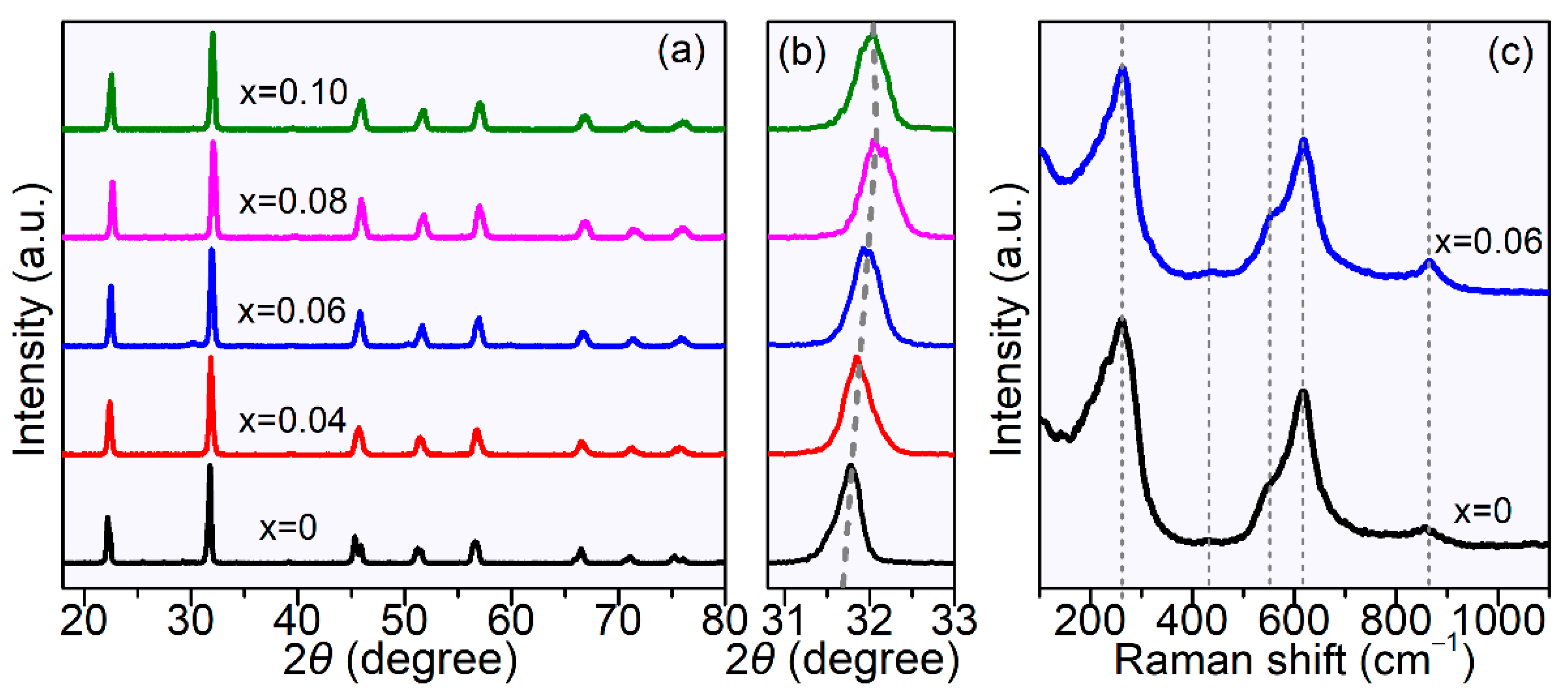
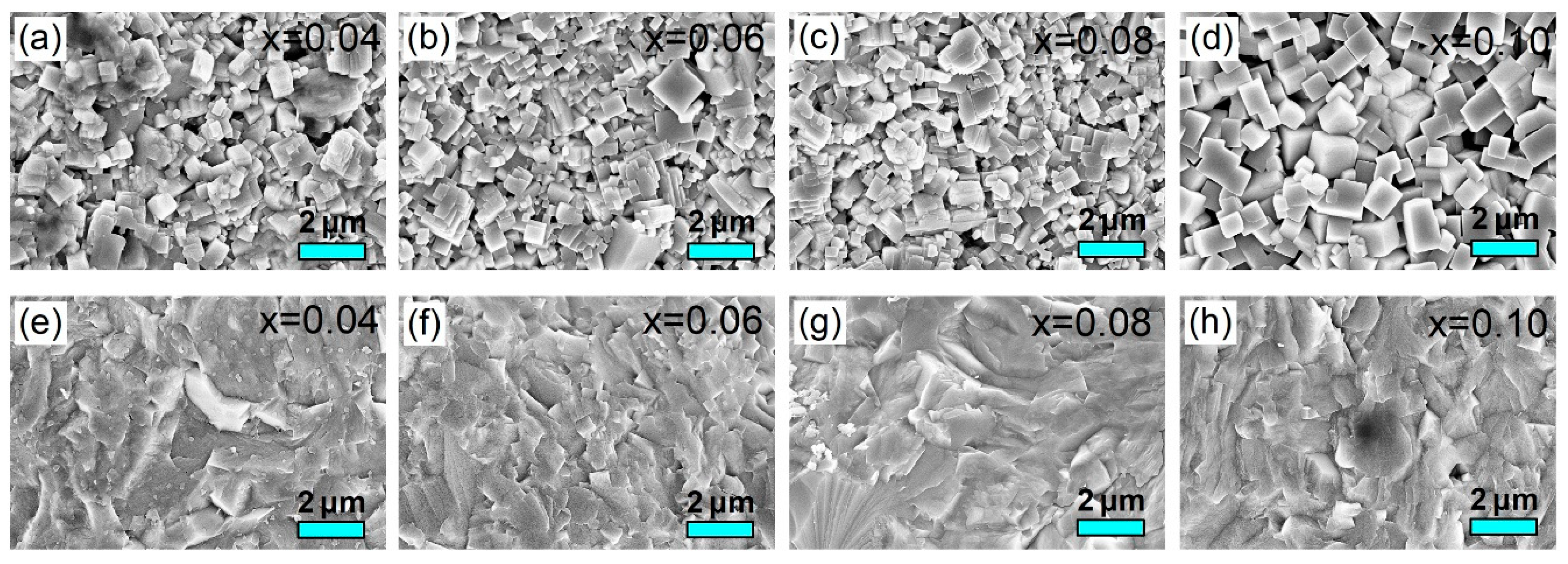
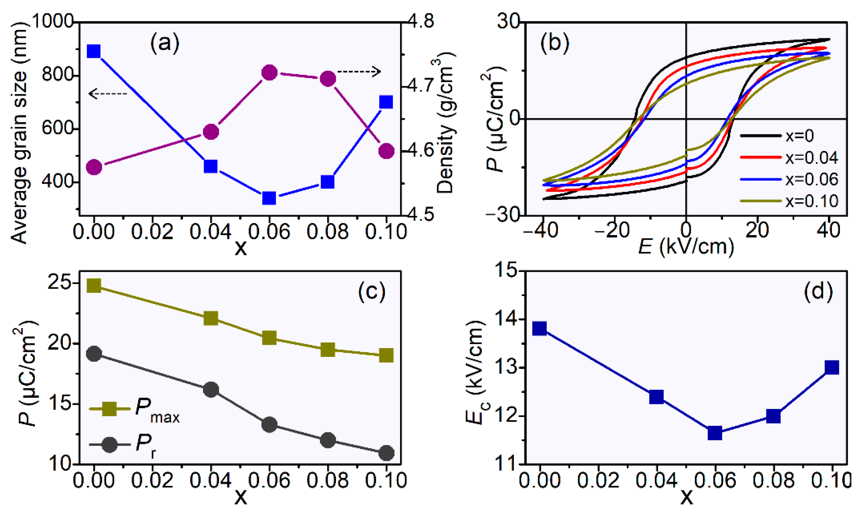
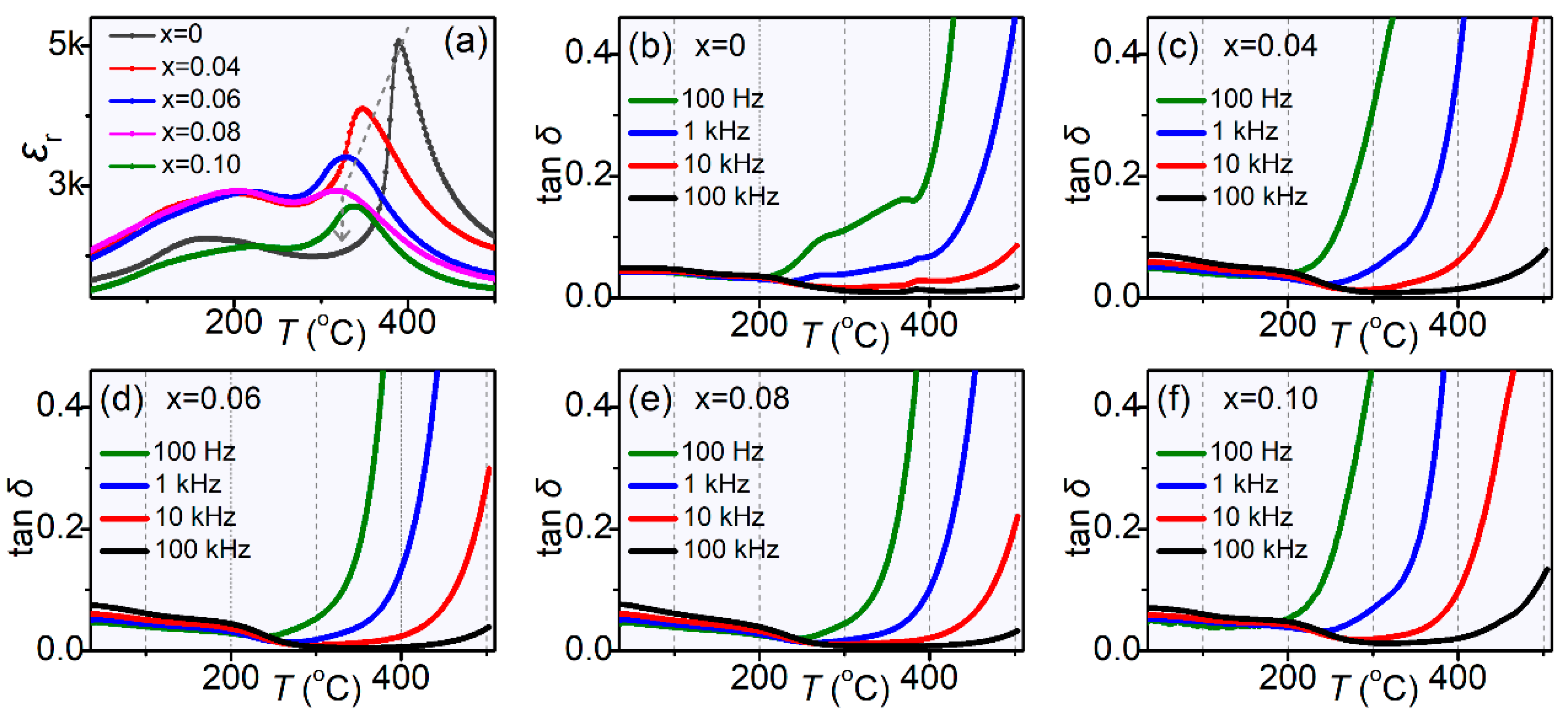
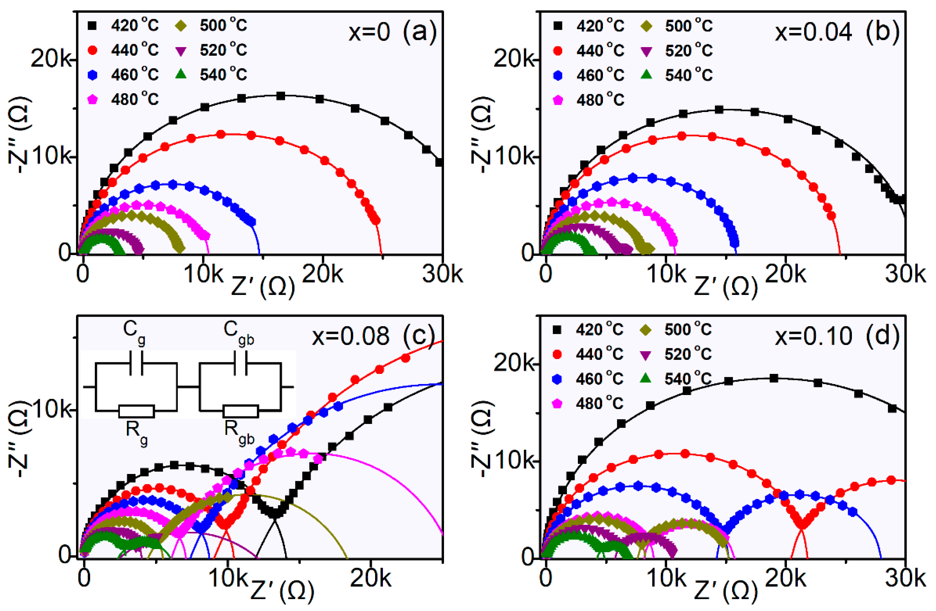
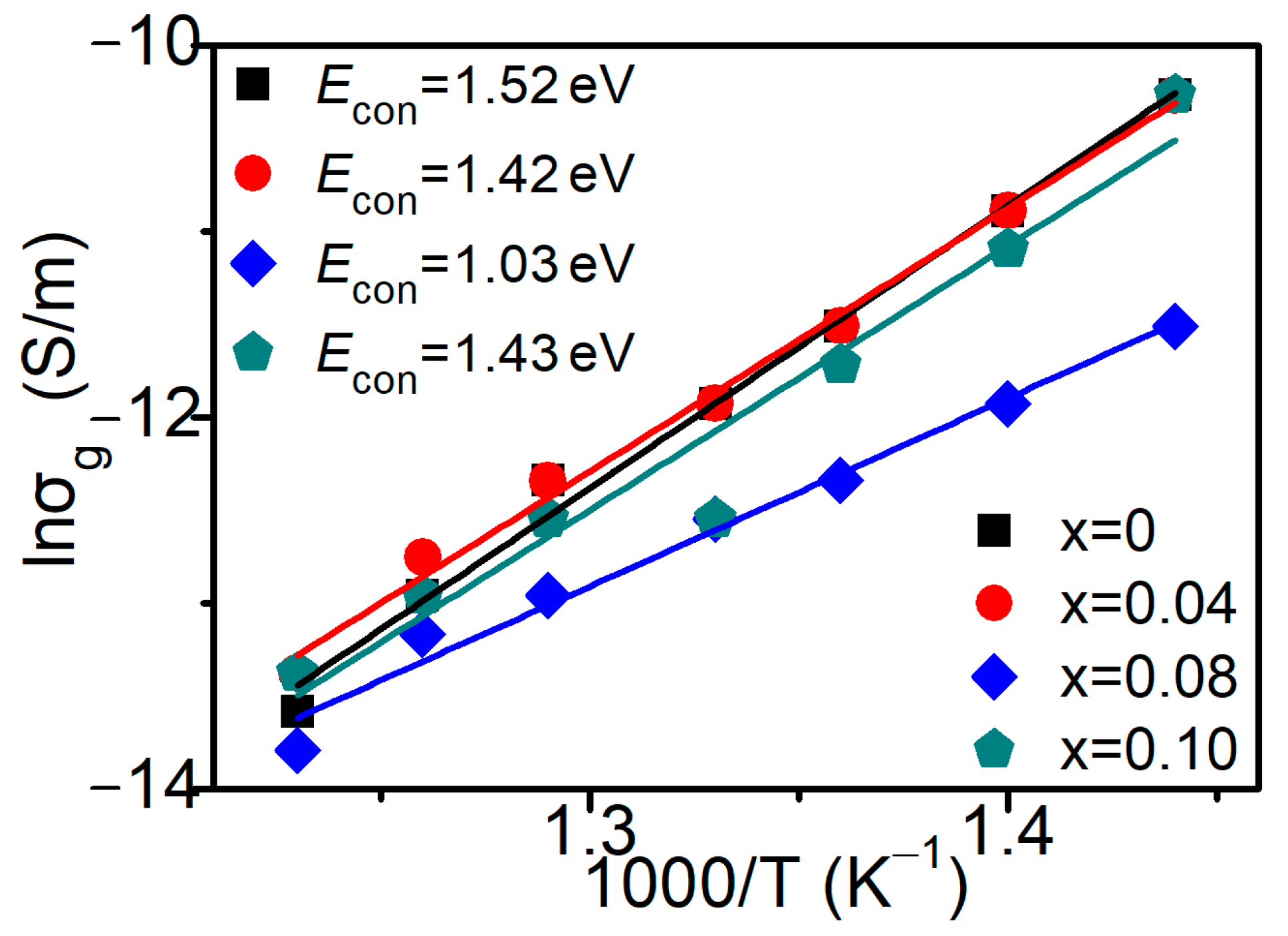
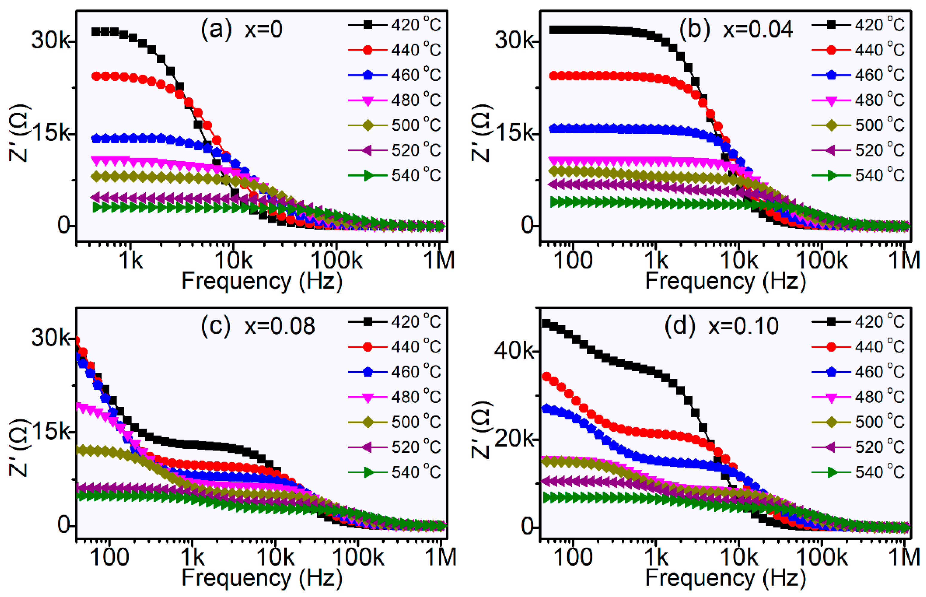
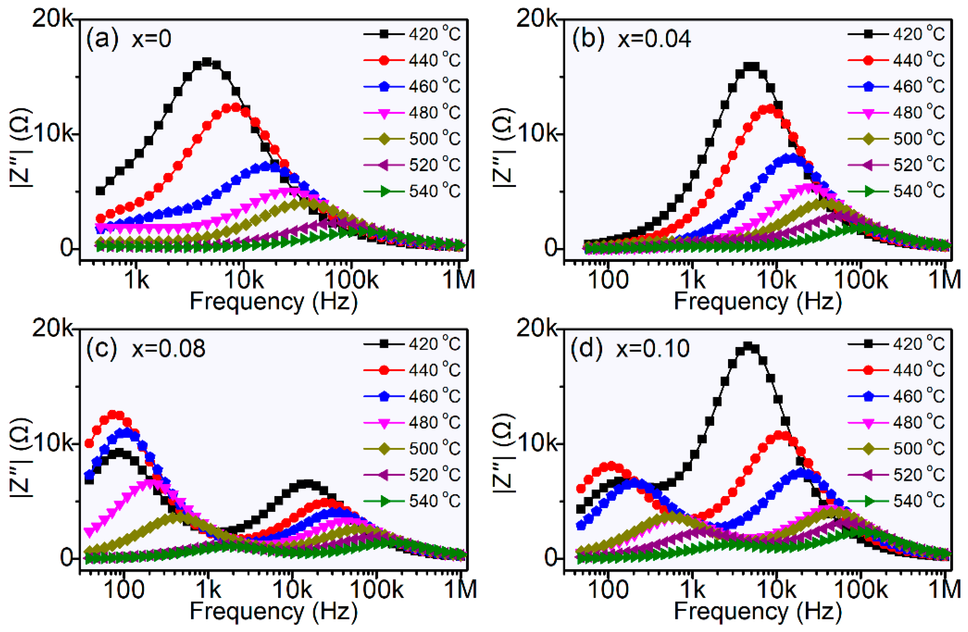
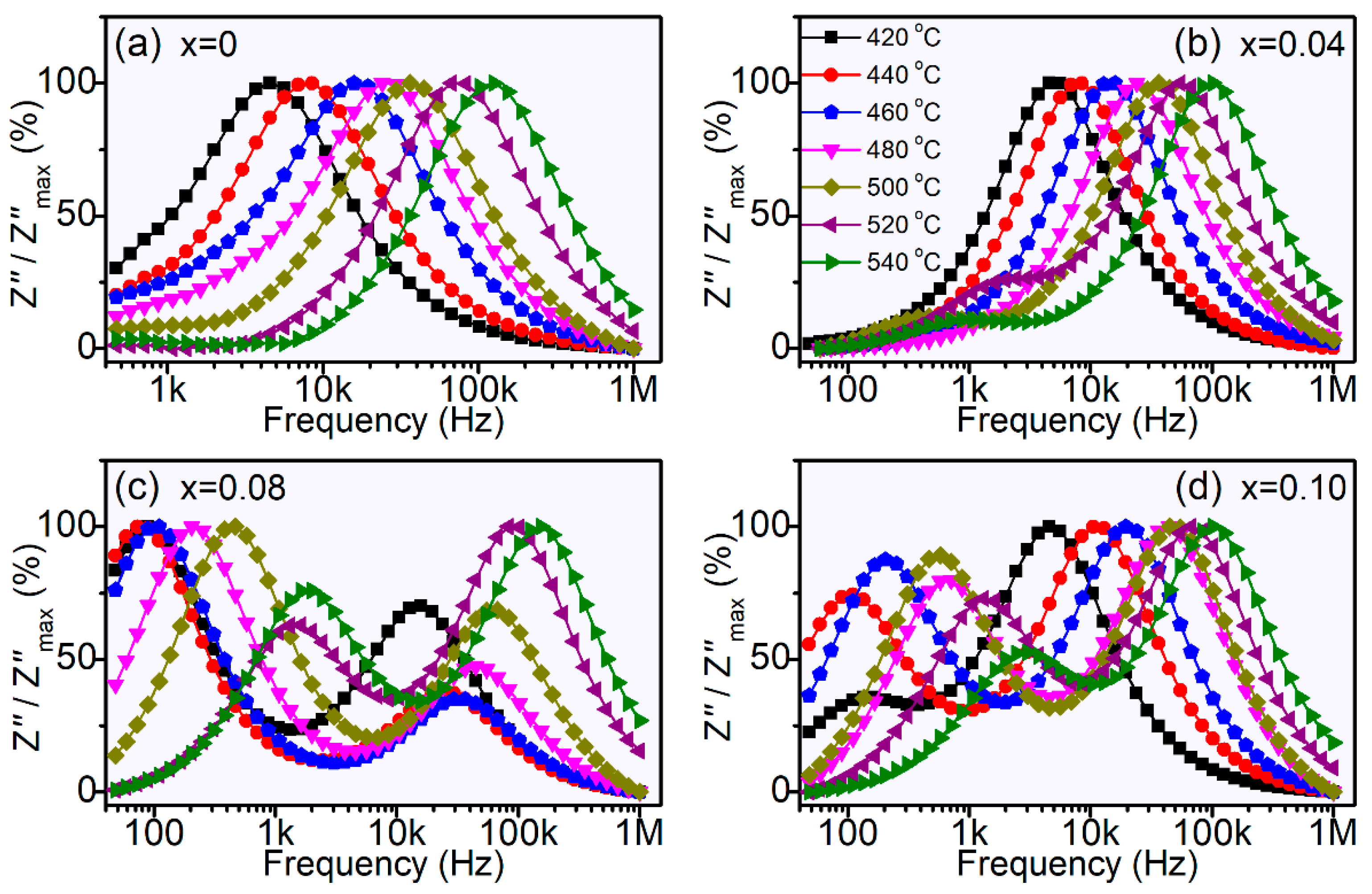
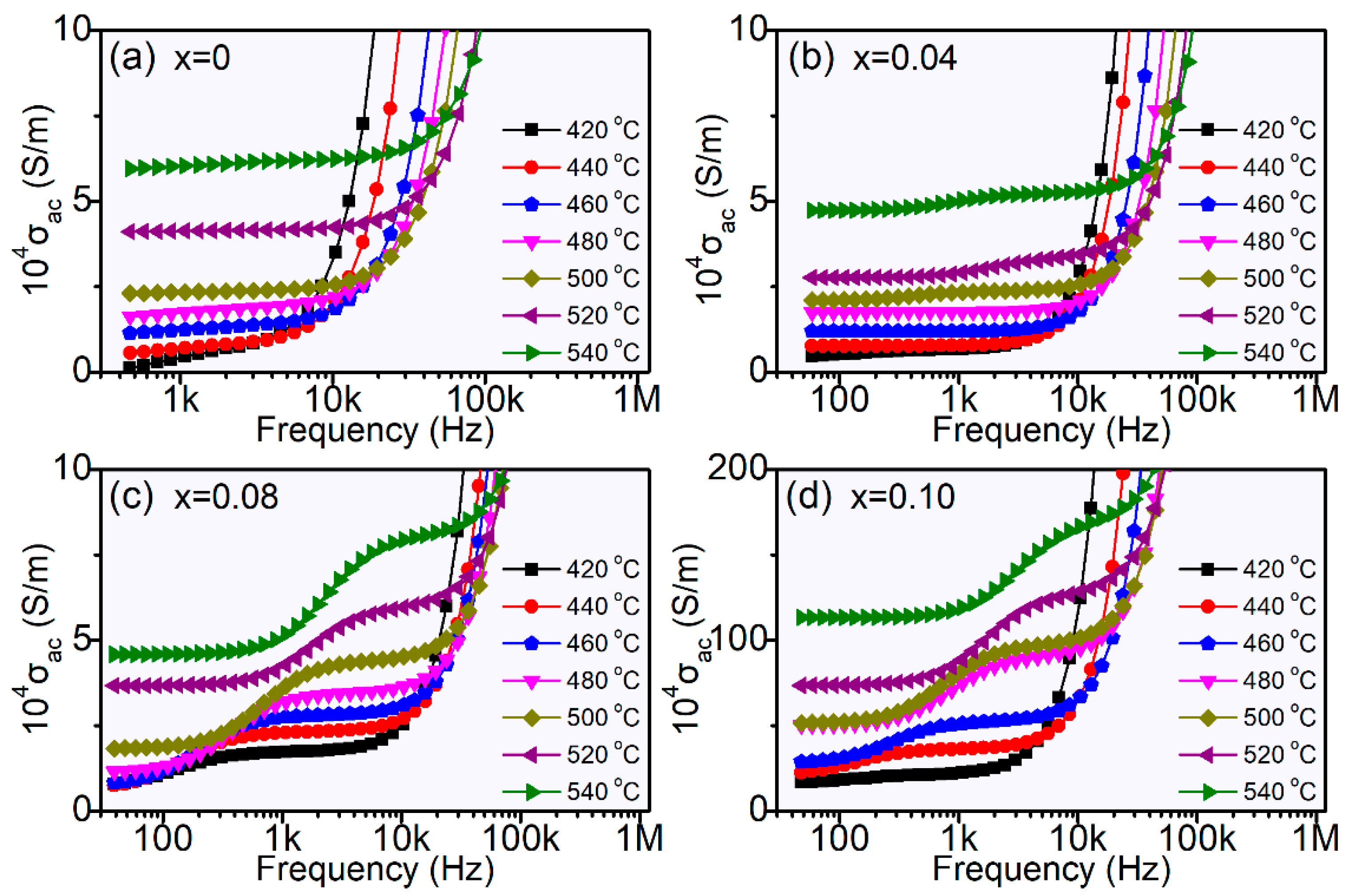
3. Results and Discussion

Figure 1a shows the XRD patterns of KNNSx-BNN ceramics measured at room temperature. All the ceramics present the pure perovskite phase without observable secondary phases, implying that all the doping ions have been well merged into the ceramic matrix to form a stable solid solution. To further judge the structure evolution, the amplified XRD patterns are also obtained and are displayed in Figure 1b. It can be seen that the peak position of XRD patterns is strongly dependent on the doping contents. With increasing x from 0 to 0.08, the diffraction peaks gradually shift to a high angle, indicating a shrinkage of unit cell and increasing lattice stress within the ceramics. It is known that the ionic radius of Sb5+ (0.60 Å) is smaller than that of Nb5+ (0.64 Å) [23], thus leading to the reduced lattice parameters when Sb is introduced into Nb sites. However, when x is further elevated to 0.10, the peak position of XRD patterns is basically the same with the sample at x = 0.08, showing no shifting diffraction peak toward a higher angle. This result indicates that there should be a solubility limit in the case of Sb doping into Nb sites, and the solubility limit here is about 0.08 in this KNN-based ceramic. After adding Sb more than this solubility limit, 0.08 Sb can enter into the B sites to replace Nb, while the rest of the Sb can only enter into the gap space between the grains as the sintering adds. Figure 1c compares the Raman spectra for KNNSx-BNN ceramics with x = 0 and x = 0.06. The observed mode peaks (i.e., ~264, ~434, ~551, ~618 and ~864 cm−1) are the characteristics of pure perovskite-structure KNN-based ceramics [24], and the mode peaks of undoped and 0.06Sb-doped ceramics present the same peak positions, also indicating the well merged doping ions into the KNN-based matrix.
Figure 2 displays the FE-SEM images of KNNSx-BNN ceramics. From Figure 2a–d, all the ceramics show the dense microstructure and nanosized and cubic-type grains. In addition, the grains of the Sb-doped ceramics under solubility limit (x = 0.04–0.08) include the small grains and relatively large grains, while the ceramic at x = 0.10 (over solubility limit) basically shows the relatively large grains with tiny amounts of small grains. This result indicates that excessive Sb doping can facilitate the grain growth as the sintering adds. From Figure 2e–h, which shows the cross-sectional microstructure, all the ceramics display transgranular fracture behavior, indicating the quite dense microstructure for KNNSx-BNN ceramics. Figure 3a gives the evolution of average grain size as a function of x for KNNSx-BNN ceramics. Before doping Sb, the average grain size of ceramic is about ~900 nm at x = 0 [22]. After introducing Sb, the average grain size decreases to ~340–400 nm at x = 0.06–0.08 and then increases again to ~700 nm at x = 0.10. This result demonstrates that the doping Sb into a KNN-based lattice can lead to the reduction of grain size, while doping more Sb will make the grain size improvement again due to the sintering-aiding effect of abundant doping ions. In this process, the density of ceramics shows the total inverse changing tendency with increasing Sb content because a lesser amount of pores and gaps will present between smaller grains. Therefore, the larger the grain size that is obtained, the lower the ceramic density will show, and the smaller the grain size that is obtained, the higher the ceramic density will show. In addition, the increasing grain boundary density caused by grain size reducing will bring about the increasing inner stress within ceramics.
Figure 3b shows the polarization–electric field (P-E) loops of KNNSx-BNN ceramics as a function of x. It can be seen that all the ceramics exhibit typical and saturated P-E loops. With increasing x, both the maximum polarization Pmax and remnant polarization Pr decreases. As shown in Figure 3c, the Pmax decreases from ~24.7 μC/cm2 (x = 0) to ~19.0 μC/cm2 (x = 0.10), and the Pr decreases from ~19.1 to ~10.9 μC/cm2 when the composition is elevated from x = 0 to x = 0.10. This result indicates that the addition of Sb will reduce the ferroelectric polarization of KNN-based ceramics [25,26]. In addition, the evolution of the coercive field Ec as a function of x is quite similar with the variation of grain size. That is, the Ec of ceramic decreases from ~13.8 kV/cm (x = 0) to ~11.7–12.0 kV/cm (x = 0.06–0.08), and then increases to ~13.0 kV/cm at x = 0.10. The large grains usually possess the large ferroelectric domains, and the large domains usually need a high electric field to switch the domains. Therefore, the coercive field is usually positively correlated with grain size.
Figure 4a shows the εr-T curves of KNNSx-BNN ceramics measured at 1 kHz. Two dielectric peaks can be clearly observed, including the paraelectric–ferroelectric phase transition temperature (Curie temperature, TC) and ferroelectric–ferroelectric phase transition temperature. With increasing x, the TC of ceramic gradually shifts to a lower temperature at x = 0–0.08, and two phase-transition dielectric peaks become broad and flat. That is, the ceramics gradually present the relaxor-like behavior after Sb doping, and the decreasing grain size also contributes to the diffusive phase transition with the broad dielectric peak. In addition, it can be seen that the TC is basically unchanged between the ceramics at x = 0.08 and x = 0.10, while the dielectric peak becomes sharper again at x = 0.10 due to its larger grains. This phenomenon is well consistent with the variation of XRD results. Figure 4b–f displays the tan δ-T curves of KNNSx-BNN ceramics measured at 100 Hz to 100 kHz. Firstly, the dielectric loss is quite similar under low temperature for different frequencies. However, the dielectric loss is small under high frequency, while it becomes quite large under low frequency, especially under a high temperature of >200 °C. That is, the dielectric loss shows the relaxor behavior with increasing frequency under high temperature. In addition, it can be seen that the relaxor range of dielectric loss gradually shifts to a higher temperature with increasing x from 0.04 to 0.08, while it decreases to low temperature again at x = 0.10. This result indicates that, at high-temperature range, the dielectric loss of KNN-based ceramics will decrease after Sb doping under solubility limit, while it increases again after doping more ions over the solubility limit. It is well known that the dielectric loss is strongly associated with the electrical conductivity of ceramics [27]. Therefore, the evolution of dielectric loss in KNNSx-BNN ceramics reflects the variation of electrical conductivity of ceramics after Sb doping. Conversely, although this system possesses a small grain size, it can be seen from Table 1 that this system shows relatively higher overall electrical (dielectric, ferroelectric and piezoelectric) properties than some other KNN-based ceramics. The electrical properties are comparable to some other lead-free and lead-based ceramics [28,29]. The comparable electrical properties make this system a promising candidate to replace lead-based ceramics.
The electrical conductivity of normal ferroelectric ceramics is quite small at low temperature, and it is difficult to observe obvious carrier migration behavior at low temperature. Therefore, the complex impedance semicircle can only be observed under relatively high temperature, at which an obvious carrier migration can happen. Thus, for most of the KNN-based ferroelectric ceramics, a high temperature of >300–400 °C is usually necessary to measure the effective complex impedance [20,22]. Figure 5 gives the complex impedances of KNNSx-BNN ceramics over 400 °C. First, it can be seen that the real impedance decreases with increasing temperature, that is, the conductivity of ceramics will increase when the temperature is elevated. Second, there is only one impedance semicircle at x = 0, and this impedance semicircle should mainly result from the grain impedance [20]. With increasing x to 0.04, there is still one impedance semicircle showing grain effect-induced impedance, while it begins to form the secondary impedance semicircle at low frequency. When x is elevated to 0.08, it can clearly see the secondary impedance semicircle at low frequency, which mainly results from the impedance induced by grain boundaries [20], and the first impedance semicircle at the high frequency region derives from the grain impedance. This result indicates that the grain and grain boundary impedances both decrease after Sb doping. That is, the electrical conductivity of grain and grain boundary both increase after Sb doping. However, with increasing x to 0.10, the grain impedance semicircle becomes big again, while the grain boundary-induced impedance semicircle becomes more observable, indicating that the grain conductivity decreases and the conductivity of the grain boundary begins to show a dominant effect on the electrical conductivity of ceramics at x = 0.10. The equivalent circuit consisting of bulk grain/grain boundary resistance (Rg and Rgb) and grain/grain boundary capacitance (Cg and Cgb) by parallel combination way (as shown in Figure 5c) was employed to evaluate the evolution of grain/grain boundary resistance, as shown in Table 2. Previous results have confirmed that grain size will decrease after Sb doping and then increase again after more Sb doping. In this process, the amounts of grain boundary will rapidly increase when grain size reduces. Therefore, the grain contribution on ceramic conductivity will decrease when grain size reduces, meanwhile the grain boundary contribution on ceramic conductivity will increase when the amounts of grain boundary increase. However, the grain contribution still shows the dominant role on ceramic conductivity when x ≤ 0.08, as shown in Figure 5a–c. After introducing more Sb with x = 0.10, the grain size increases again; therefore, the grain conductivity decreases. Because the redundant doping Sb will enter into the grain boundary when x = 0.10, which can facilitate the conductivity of grain boundary, the conductivity of the grain boundary still increases and shows a dominant role on ceramic conductivity at high temperature although the amounts of grain boundary become less, as shown in Figure 5d. The increasing conductivity of the grain and grain boundary can facilitate the carrier migration, and can thus lead to improvement of the dielectric property. From Figure 4a, the evolution of a room-temperature dielectric constant is quite similar with the variation of grain and grain boundary conductivity for KNNSx-BNN ceramics.
For figuring out the origin of conductivity variation, the activation energy of grain conductivity is carried out according to the Arrhenius equation [20],
𝜎g = 𝜎0 exp (−𝐸con/𝑘B𝑇)
where 𝜎g and 𝜎0 are the conductivity and initial conductivity of the grain, 𝑘B is the Boltzmann constant, 𝑇 is the absolute temperature, and Econ is the conductance activation energy. As shown in Figure 6, it can be seen that the activation energy first decreases from 1.52 to 1.03 eV when the content of doping Sb increases from x = 0 to x = 0.08, and then, the activation energy increases again to 1.43 eV with increasing Sb doping content to x = 0.10. The high activation energy indicates that the migration for carriers is difficult; thus, the impedance/resistance is large and the electrical conductivity will be low, and vice versa. Therefore, the doping Sb can lead to a decrease in activation energy for the ceramic grain, and the large grain usually possesses the higher activation energy.
Figure 7 shows the real parts of impedances (resistance) for KNNSx-BNN ceramics. The low-frequency resistance region is mainly decided by the DC electrical conductivity, and the high-frequency resistance region is mainly contributed by the AC electrical conductivity of ceramics [30]. It can be seen that the low-frequency resistance is obviously higher than the high-frequency resistance, implying that the electrical conductivity will sharply increase when the dominating conductivity contribution is changed from DC conductivity to AC conductivity with increasing frequency. However, this difference between low-frequency resistance and high-frequency resistance will become small at quite a high temperature. In addition, the low-frequency DC resistance region is flat for the compositions at x = 0 and 0.04, and the flat resistance region gradually becomes broad when the temperature is elevated, indicating that the DC conductivity of ceramics becomes more obvious and can present a wider frequency range under high temperature. However, with increasing x to 0.08, the low-frequency resistance region becomes sensitive to the frequency variation, especially at relatively low temperature. This result indicates that there is complex conductivity contribution when the content of doping Sb is close to the solubility limit. Due to the smaller grains with increasing doping content, the complex conductivity contribution should result from the obvious grain boundary effect on ceramic conductivity. Nevertheless, the frequency sensitivity of resistance decreases again at x = 0.10. The low-frequency resistance increases and tends to become flat under the low frequency region because of the improvement grain size and reduced grain boundary effect at x = 0.10.
Figure 8 displays the imaginary part of impedance (reactance) for KNNSx-BNN ceramics. It can be seen that the imaginary part of the impedance first increases and then decreases with increasing frequency from low to high values at x = 0 and 0.04. Furthermore, the reactance peak gradually becomes low and shifts to a high frequency region when the measuring temperature is elevated. This phenomenon indicates that the reactance shows relaxation behavior. For the composition at x = 0.08, two reactance peaks can be seen. There is a new reactance peak in the low-frequency region. According to the above result, the grain boundary contribution is significant in this composition; thus, this new reactance peak should mainly derive from the grain boundary contribution. Therefore, the reactance peak at medium frequency should mainly result from the grain contribution. When the composition is elevated from x = 0.04 to x = 0.08, it was found that the peak intensity of medium-frequency reactance decreases, while the low-frequency reactance peak is quite obvious. That is, the grain boundary contribution becomes significant for ceramic reactance. When the composition is elevated to x = 0.10, the low-frequency reactance peak is also obvious, while the medium-frequency reactance peak increases again, indicating the improving grain contribution again, which is well consistent with the above results.
For further clarity illustrating the frequency dependence of impedance, the normalized imaginary part of impedance (normalized reactance) was obtained, as shown in Figure 9. Firstly, there is only one normalized reactance peak at x = 0 (Figure 9a). According to the above results, this peak is mainly contributed by grain conductivity. After introducing Sb, an emerging new reactance peak appears in low frequency and high temperature at x = 0.04 (Figure 9b). When the content of doping Sb is elevated to x = 0.08 and 0.10, the low-frequency normalized reactance peak can be clearly observed (Figure 9c,d). This phenomenon indicates that the grain boundary conductivity actually begins to show an observable contribution at high temperature from x = 0.04 and then possesses a significant contribution at x = 0.08 and 0.10. This result implies that partial doping Sb ions have entered into the grain boundary from x = 0.04, thus leading to the increasing grain boundary conductivity after Sb doping. Conversely, the low-frequency side of the normalized reactance peak is mainly contributed by DC conductivity, and the high-frequency side of the normalized reactance peak is mainly contributed by AC conductivity [31]. It can be seen that both of the low-frequency and medium-frequency reactance peaks gradually shift to a high-frequency region when the measuring temperature is elevated, demonstrating that the DC conductivity becomes more obvious and can present in a broader frequency range at high temperature due to both the grain and grain boundary contribution.
Figure 10 gives the AC conductivity (σac) as a function of temperature and frequency. There is one flat conductivity region at the low-frequency range for the composition at x = 0 and 0.04. This flat conductivity region indicates that the long-range motion of the carrier dominates the conductivity in this frequency range [32]. When the composition is elevated to x = 0.08 and 0.10, two conductivity flats can be observed in the low-frequency range. These two flats should result from the grain and grain boundary contribution after high-content Sb doping based on the above results. With increasing the frequency over the flat conductivity region, the σac of all the ceramics increases sharply to a large value, and the critical frequency is about ~10 kHz when the ceramics have high AC conductivity. Under this state, the ceramic conductivity mainly results from short-range carrier jumping. In addition, it was found that the AC conductivity of ceramic at x = 0.10 is much higher than the ceramic at x = 0-0.08. The prominent grain boundary conductivity as well as the high grain conductivity should contribute to this result. For the ceramics at x = 0-0.08, although the grain boundary conductivity gradually increases with increasing doping content, it is still more inferior than the ceramic at x = 0.10.

4. Conclusions

The fine-grain KNNSx-BNN ceramics were prepared by the conventional solid method, and then, the effects of Sb doping on the electrical conductivity were systemically investigated. The grain size first decreases below the solubility limit and then increases again after doping more Sb over the solubility limit. With the grain size variation, the dielectric loss, coercive field, grain resistance and its activation energy present a similar changing tendency. However, since the density of the grain boundary will increase when the grain size decreases and the doping ions can enter into grain boundary, the grain boundary conductivity steadily increases after Sb doping. Consequently, the grain contribution on ceramic conductivity changes with grain size variation, while the grain boundary contribution becomes more obvious with increasing doping content. This work reveals the effects of Sb doping on the electrical conductivity in KNN-based ferroelectric ceramics.

Author Contributions

Conceptualization, C.Z. and C.L.; methodology, J.J.; formal analysis, J.J. and S.C.; resources, C.Z. and C.L.; writing—original draft preparation, J.J.; writing—review and editing, J.J., C.Z. and C.L.; visualization, S.C., X.W., T.L., M.G. and C.F.; supervision, X.W., T.L., M.G. and C.F.; project administration, C.Z. and C.L. All authors have read and agreed to the published version of the manuscript.

Funding

The authors gratefully acknowledge the support of the National Natural Science Foundation of China (nos. 52072075, 12104093 and 52102126), the Natural Science Foundation of Fujian Province (nos. 2021J05122, 2021J05123, 2022J01087 and 2022J01552) and Qishan Scholar Financial Support from Fuzhou University (GXRC-20099).

Data Availability Statement

The data and materials that support the findings of this study are available from the corresponding author upon reasonable request.

Conflicts of Interest

The authors declare no conflict of interest.

References

  1. Wu, J. Advances in Lead-Free Piezoelectric Materials; Springer: Berlin/Heidelberg, Germany, 2018. [Google Scholar]
  2. Lv, X.; Zheng, T.; Zhao, C.; Yin, J.; Wu, H.; Wu, J. Multiscale Structure Engineering for High-Performance Pb-Free Piezoceramics. Acc. Mater. Res. 2022, 3, 461–471. [Google Scholar] [CrossRef]
  3. Zhao, C.; Huang, Y.; Wu, J. Multifunctional barium titanate ceramics via chemical modification tuning phase structure. InfoMat 2020, 2, 1163–1190. [Google Scholar] [CrossRef]
  4. Huang, Y.; Zhao, C.; Wu, B.; Zhang, X. Grain size effects and structure origin in high-performance BaTiO3-based piezoceramics with large grains. J. Eur. Ceram. Soc. 2022, 42, 2764–2771. [Google Scholar] [CrossRef]
  5. Tao, H.; Yin, J.; Zhao, C.; Wu, B.; Zhao, L.; Ma, J.; Wu, J. Large electrocaloric effect under electric field behavior in potassium sodium niobate ceramics with incompletely overlapped phase boundaries. J. Mater. Chem. A 2022, 10, 5262–5272. [Google Scholar] [CrossRef]
  6. Wei, X.; Zhao, C.; Zheng, T.; Lv, X.; Zhang, L.; Li, B.; Wu, J. Understanding the enhanced electrocaloric effect in BaTiO3-based ferroelectrics at critical state. Acta Mater. 2022, 227, 117735. [Google Scholar] [CrossRef]
  7. Zhong, S.; Zhao, C.; Li, B.; Zhang, L.; Huang, Y.; Wu, J. Tuning the electrocaloric effect by tailoring phase fraction in BaTiO3-based ferroelectrics. J. Eur. Ceram. Soc. 2022, 42, 5172–5178. [Google Scholar] [CrossRef]
  8. Rao, G.; Fang, H.; Zhou, T.; Zhao, C.; Shang, N.; Huang, J.; Liu, Y.; Du, X.; Li, P.; Jian, X. Robust Piezoelectricity with Spontaneous Polarization in Monolayer Tellurene and Multilayer Tellurium Film at Room Temperature for Reliable Memory. Adv. Mater. 2022, 34, 2204697. [Google Scholar] [CrossRef]
  9. Lv, X.; Zhu, J.; Xiao, D.; Zhang, X.-X.; Wu, J. Emerging new phase boundary in potassium sodium-niobate based ceramics. Chem. Soc. Rev. 2020, 49, 671–707. [Google Scholar] [CrossRef]
  10. Xing, J.; Chen, H.; Jiang, L.; Zhao, C.; Tan, Z.; Huang, Y.; Wu, B.; Chen, Q.; Xiao, D.; Zhu, J. High performance BiFe0.9Co0.1O3 doped KNN-based lead-free ceramics for acoustic energy harvesting. Nano Energy 2021, 84, 105900. [Google Scholar] [CrossRef]
  11. Deng, B.; Jiang, J.; Li, H.; Zhao, C.; Lin, C.; Wu, X.; Gao, M.; Lin, T. Enhanced piezoelectric property in Mn-doped K0.5Na0.5NbO3 ceramics via cold sintering process and KMnO4 solution. J. Am. Ceram. Soc. 2022, 105, 5774–5782. [Google Scholar] [CrossRef]
  12. Ma, Y.; Yang, S.; Zhao, C.; Lin, C.; Lin, J.; Wu, X.; Gao, M.; Lin, T.; Fang, C. Photochromic and Electric Field-Regulating Luminescence in High-Transparent (K, Na)NbO3-Based Ferroelectric Ceramics with Two-Phase Coexistence. ACS Appl. Mater. Interfaces 2022, 14, 35940–35948. [Google Scholar] [CrossRef]
  13. Wu, B.; Ma, J.; Tao, H.; Zhao, L.; Wang, X.; Wu, W.; Zhao, C. Evolution of Multilevel Structures and Electrical properties in Potassium-Sodium Niobate-Based Lead-Free Piezoceramics by Anionic Fluorine Engineering. J. Alloys Compd. 2022, 918, 165604. [Google Scholar] [CrossRef]
  14. Wu, X.; Lin, J.; Xu, Z.; Zhao, C.; Lin, C.; Wang, H.; Lin, T.; Zheng, X.; Sa, B.; Zhang, Q.; et al. Defect Management and Multi-Mode Optoelectronic Manipulations via Photo-Thermochromism in Smart Windows. Laser Photonics Rev. 2021, 15, 2100211. [Google Scholar] [CrossRef]
  15. Deng, B.; Ma, Y.; Chen, T.; Wang, H.; Lin, J.; Lin, C.; Wu, X.; Zhao, C.; Lin, T.; Gao, M.; et al. Elevating electrical properties of (K, Na)NbO3 ceramics via cold sintering process and post-annealing. J. Am. Ceram. Soc. 2022, 105, 461–468. [Google Scholar] [CrossRef]
  16. Wang, H.; Lin, J.; Deng, B.; Lin, T.; Lin, C.; Cheng, Y.; Wu, X.; Zheng, X.; Yu, X. Reversible multi-mode modulations of optical behavior in photochromic-translucent Nd-doped K0.5Na0.5NbO3 ceramics. J. Mater. Chem. C 2020, 8, 2343–2352. [Google Scholar] [CrossRef]
  17. Wu, J.; Xiao, D.; Zhu, J. Potassium-sodium niobate lead-free piezoelectric materials: Past, present, and future of phase boundaries. Chem. Rev. 2015, 115, 2559–2595. [Google Scholar] [CrossRef] [PubMed]
  18. Liao, Y.; Wang, D.; Wang, H.; Wang, T.; Zheng, Q.; Yang, J.; Kwok, K.; Lin, D. Transformation of hardening to softening behaviors induced by Sb substitution in CuO-doped KNN-based piezoceramics. Ceram. Int. 2019, 45, 13179–13186. [Google Scholar] [CrossRef]
  19. Gao, X.; Cheng, Z.; Chen, Z.; Liu, Y.; Meng, X.; Zhang, X.; Wang, J.; Guo, Q.; Li, B.; Sun, H. The mechanism for the enhanced piezoelectricity in multi-elements doped (K, Na)NbO3 ceramics. Nat. Commun. 2021, 12, 881. [Google Scholar] [CrossRef]
  20. Wang, X.; Huan, Y.; Wang, Z.; Lin, X.; Huang, S.; Wei, T.; Li, L.; Wang, X. Electrical conduction and dielectric relaxation mechanisms in the KNN-based ceramics. J. Appl. Phys. 2019, 126, 104101. [Google Scholar] [CrossRef]
  21. Rafiq, M.A.; Costa, M.E.; Tkach, A.; Vilarinho, P.M. Impedance analysis and conduction mechanisms of lead free potassium sodium niobate (KNN) single crystals and polycrystals: A comparison study. Cryst. Growth Des. 2015, 15, 1289–1294. [Google Scholar] [CrossRef]
  22. Jiang, J.; Li, H.; Zhao, C.; Lin, C.; Wu, X.; Lin, T.; Gao, M.; Wang, Z. Broad-temperature-span and improved piezoelectric/dielectric properties in potassium sodium niobate-based ceramics through diffusion phase transition. J. Alloys Compd. 2022, 925, 166708. [Google Scholar] [CrossRef]
  23. Zhang, Y.; Li, J.-F. Review of chemical modification on potassium sodium niobate lead-free piezoelectrics. J. Mater. Chem. C 2019, 7, 4284–4303. [Google Scholar] [CrossRef]
  24. Zheng, T.; Wu, H.; Yuan, Y.; Lv, X.; Li, Q.; Men, T.; Zhao, C.; Xiao, D.; Wu, J.; Wang, K. The structural origin of enhanced piezoelectric performance and stability in lead free ceramics. Energy Environ. Sci. 2017, 10, 528–537. [Google Scholar] [CrossRef]
  25. Liu, Q.; Zhang, Y.; Gao, J.; Zhou, Z.; Wang, H.; Wang, K.; Zhang, X.; Li, L.; Li, J.-F. High-performance lead-free piezoelectrics with local structural heterogeneity. Energy Environ. Sci. 2018, 11, 3531–3539. [Google Scholar] [CrossRef]
  26. Zhao, C.; Wu, B.; Wang, K.; Li, J.-F.; Xiao, D.; Zhu, J.; Wu, J. Practical high strain with superior temperature stability in lead-free piezoceramics through domain engineering. J. Mater. Chem. A 2018, 6, 23736–23745. [Google Scholar] [CrossRef]
  27. Liu, G.; Zhang, S.; Jiang, W.; Cao, W. Losses in ferroelectric materials. Mater. Sci. Eng. R 2015, 89, 1–48. [Google Scholar] [CrossRef] [PubMed]
  28. Hajra, S.; Sahoo, S.; De, M.; Rout, P.K.; Tewari, H.S.; Choudhary, R.N.P. Structural and electrical characteristics of barium modified bismuth-sodium titanate (Bi0.49Na0.49Ba0.02)TiO3. J. Mater. Sci. Mater. Electron. 2018, 29, 1463–1472. [Google Scholar] [CrossRef]
  29. Sharma, P.; Hajra, S.; Sahoo, S.; Rout, P.K.; Choudhary, R.N.P. Structural and electrical characteristics of gallium modified PZT ceramics. Process. Appl. Ceram. 2017, 11, 171–176. [Google Scholar] [CrossRef]
  30. Abdullah, M.; Yusoff, A. Complex impedance and dielectric properties of an Mg-Zn ferrite. J. Alloys Compd. 1996, 233, 129–135. [Google Scholar] [CrossRef]
  31. Kumari, P.; Rai, R.; Kholkin, A.L. Influence of BiFeTaO3 addition on the electrical properties of Na0.4725K0.4725Li0.055NbO3 ceramics system using impedance spectroscopy. J. Alloys Compd. 2015, 637, 203–212. [Google Scholar] [CrossRef]
  32. Chen, X.; Xiao, Y.; Li, X.; Liu, G.; Sun, J.; Xu, L.; Zhou, H. Excellent temperature stability on relative permittivity, and conductivity behavior of K0.5Na0.5NbO3 based lead free ceramics. J. Alloys Compd. 2018, 762, 697–705. [Google Scholar] [CrossRef]
Figure 1. Composition-dependent (a) XRD patterns and (b) expanded patterns of KNNSx-BNN ceramics. (c) Raman spectra for KNNSx-BNN ceramics with x = 0 and x = 0.06.
Crystals 12 01311 g001
Figure 2. (ad) Surface and (eh) cross-sectional FE-SEM images of KNNSx-BNN ceramics.
Crystals 12 01311 g002
Figure 3. (a) Evolution of average grain size as a function of x for KNNSx-BNN ceramics. (b) Composition-dependent P-E loops of KNNSx-BNN ceramics. Evolution of (c) Pmax and Pr and (d) Ec as a function of x for KNNSx-BNN ceramics.
Crystals 12 01311 g003
Figure 4. (a) Composition-dependent εr-T curves as a function of x for KNNSx-BNN ceramics. Temperature/frequency dependence of tan δ-T curves of KNNSx-BNN ceramics with (b) x = 0, (c) x = 0.04, (d) x = 0.06, (e) x = 0.08 and (f) x = 0.10.
Crystals 12 01311 g004
Figure 5. Temperature-dependent complex impedances for KNNSx-BNN ceramics with (a) x = 0, (b) x = 0.04, (c) x = 0.08 and (d) x = 0.10 measured at high temperature.
Crystals 12 01311 g005
Figure 6. Arrhenius plots and fitting results as well as corresponding activation energy of grain conductivity for KNNSx-BNN ceramics.
Crystals 12 01311 g006
Figure 7. Frequency/temperature-dependent real parts of impedances for KNNSx-BNN ceramics with (a) x = 0, (b) x = 0.04, (c) x = 0.08 and (d) x = 0.10 measured at high temperature.
Crystals 12 01311 g007
Figure 8. Frequency/temperature-dependent imaginary parts of impedances for KNNSx-BNN ceramics with (a) x = 0, (b) x = 0.04, (c) x = 0.08 and (d) x = 0.10 measured at high temperature.
Crystals 12 01311 g008
Figure 9. Frequency/temperature-dependent normalized imaginary parts of impedances for KNNSx-BNN ceramics with (a) x = 0, (b) x = 0.04, (c) x = 0.08 and (d) x = 0.10 measured at high temperature.
Crystals 12 01311 g009
Figure 10. Frequency/temperature-dependent AC electrical conductivity for KNNSx-BNN ceramics with (a) x = 0, (b) x = 0.04, (c) x = 0.08 and (d) x = 0.10 measured at high temperature.
Crystals 12 01311 g010
Table 1. Comparison of grain size, εr, Pr and piezoelectric coefficient d33 between this system and other fine-grain KNN-based ceramics prepared by the traditional solid-state method.
SystemGrain Size (nm)εrPr (μC/cm2)d33 (pC/N)Refs.
KNLNS-BZ-BNH-Fe~1000~3500~14.0-[5]
KNN~1700~460~12.7~75[11]
F-doped KNN-~320~10.1~147[13]
Er-KNN-BST~200~1300--[14]
KNN-BNN-Ce~600~700~18.0~170[22]
KNN-BNW~370~1000--[30]
KNNS0.04-BNN~460~1700~17.0~100This work
Table 2. Temperature-dependent resistance of grain and grain boundary for KNNSx-BNN ceramics.
Temperature (°C)x = 0x = 0.04x = 0.08x = 0.10
Rg (Ω)Rgb (Ω)Rg (Ω)Rgb (Ω)Rg (Ω)Rgb (Ω)Rg (Ω)Rgb (Ω)
42033,000-30,600-14,10048,00038,000-
44024,900-24,500-10,40039,00021,90017,500
46014,700-15,800-870033,00015,20013,600
48010,500-10,800-710019,70090007600
5008100-8030-550013,80083007500
5204600-5800-4000970067004800
5403100-3600-2900370049002500
Publisher’s Note: MDPI stays neutral with regard to jurisdictional claims in published maps and institutional affiliations.

