
Design of Semiconductor Contact Grating Terahertz Source with Enhanced Diffraction Efficiency


Abstract
:1. Introduction
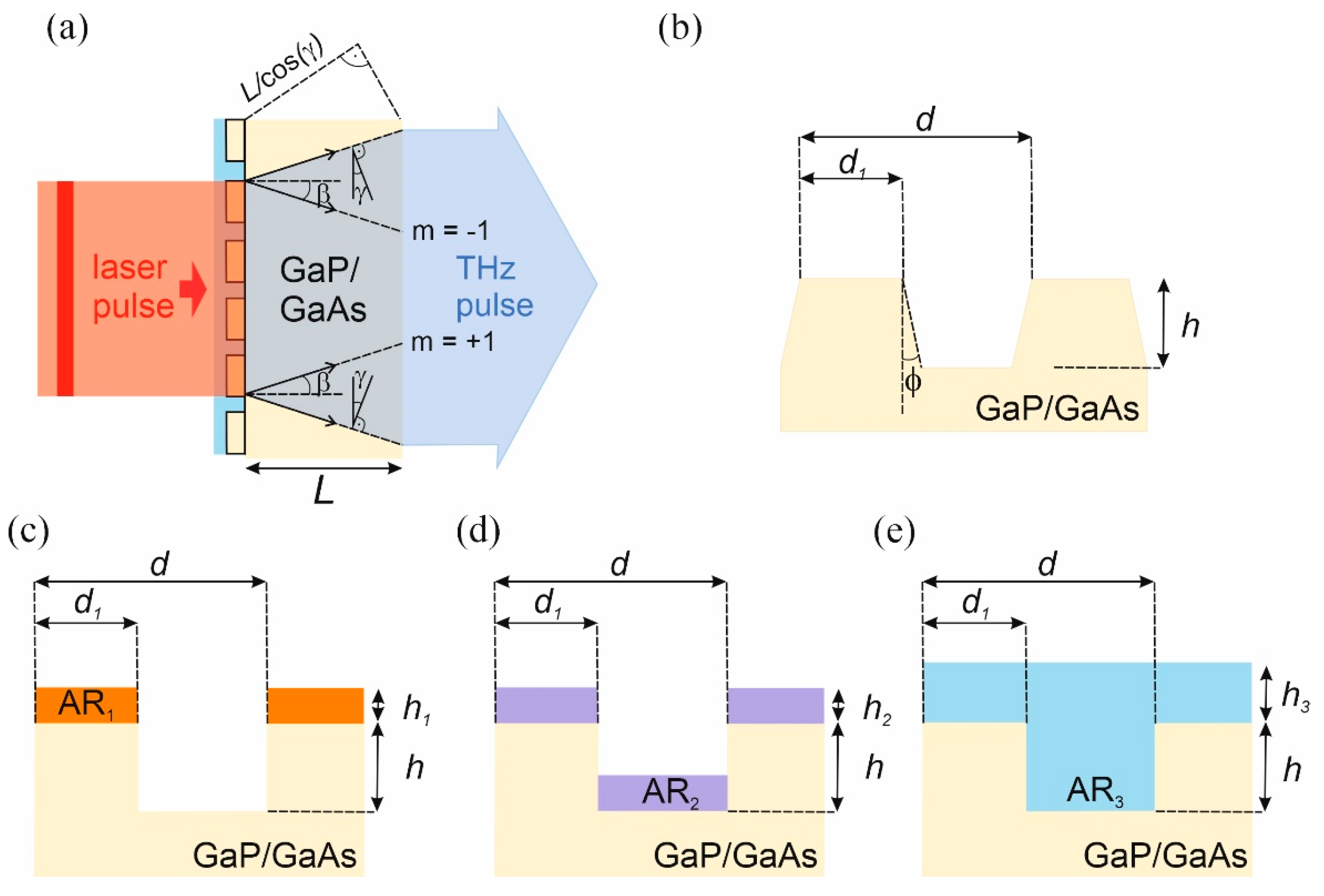
2. Grating Design
3. Results
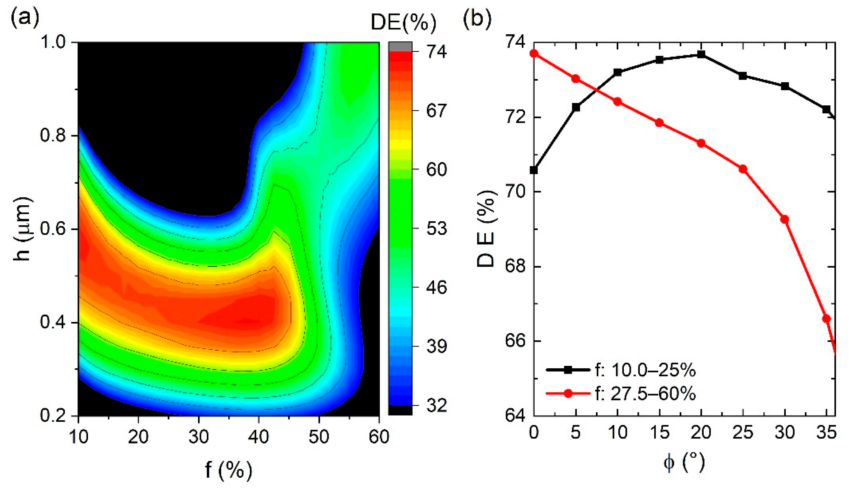
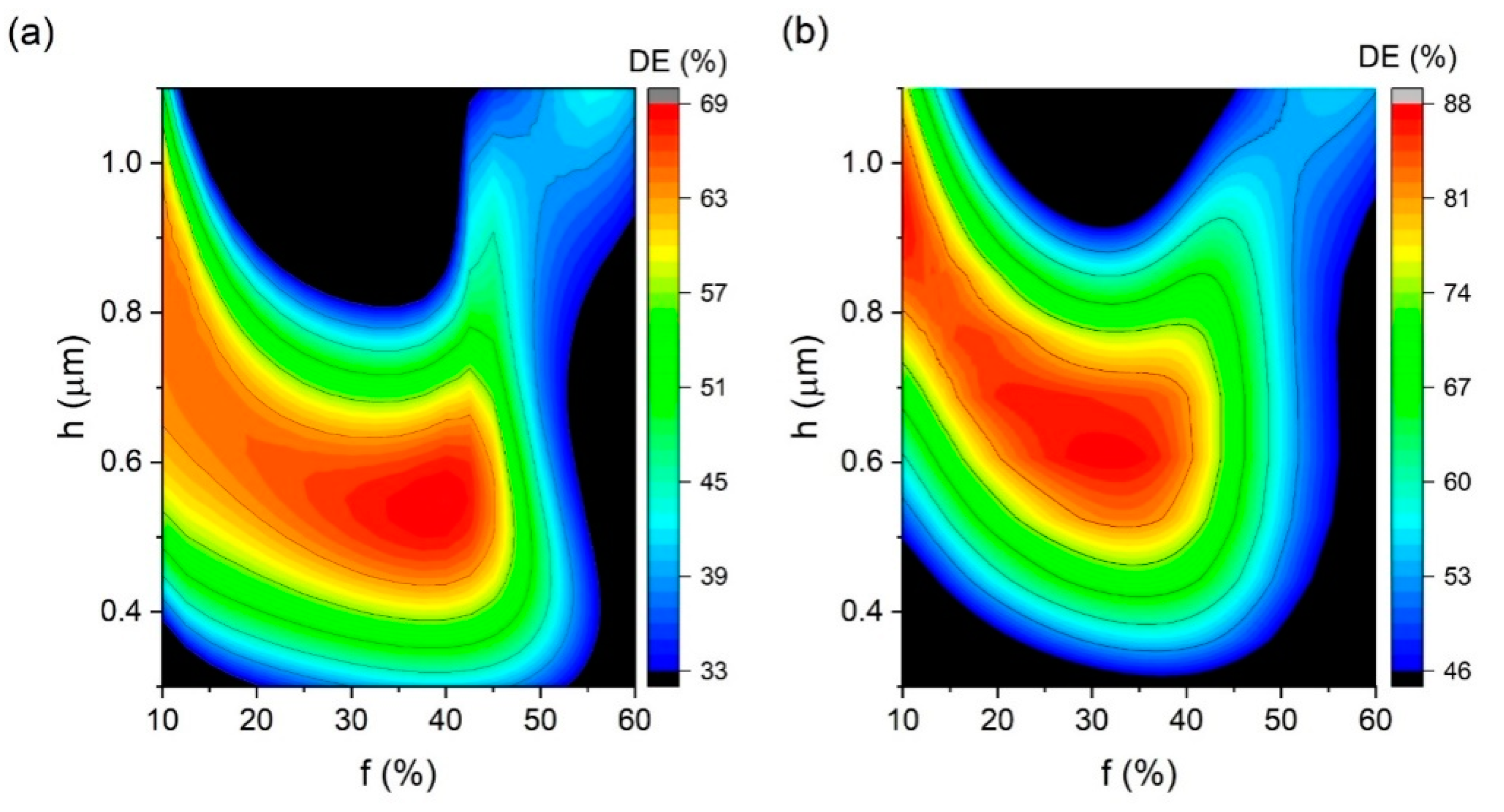
3.1. Effect of Wall Angle on Diffraction Efficiency
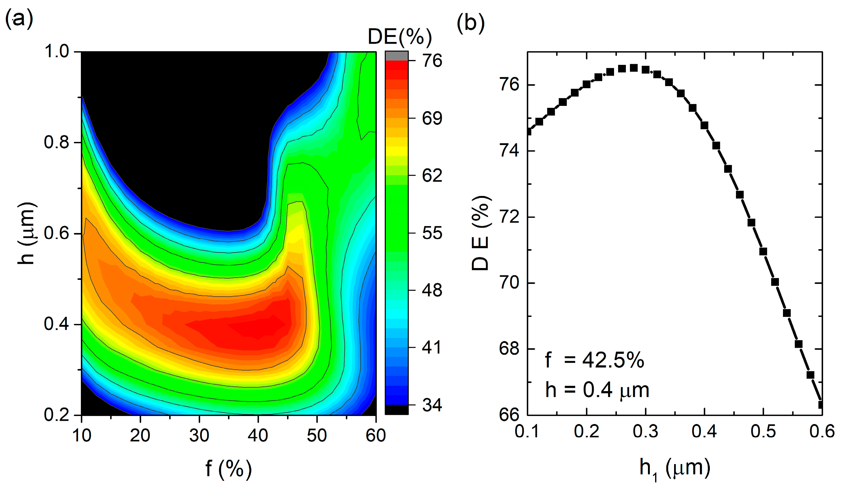
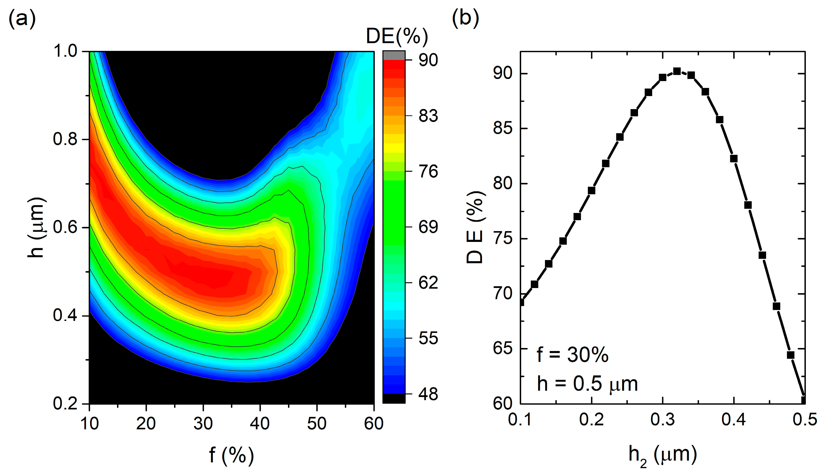
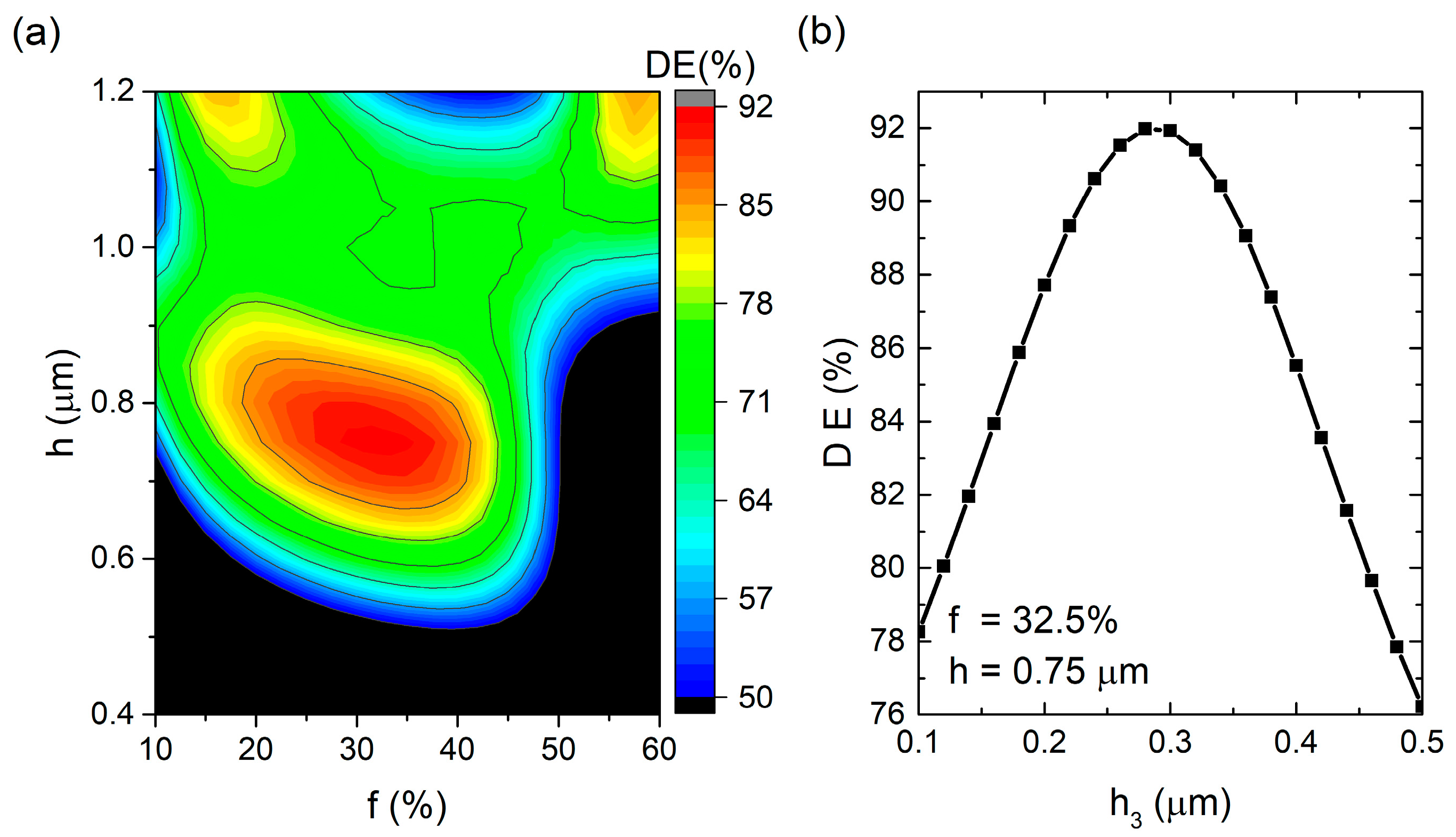
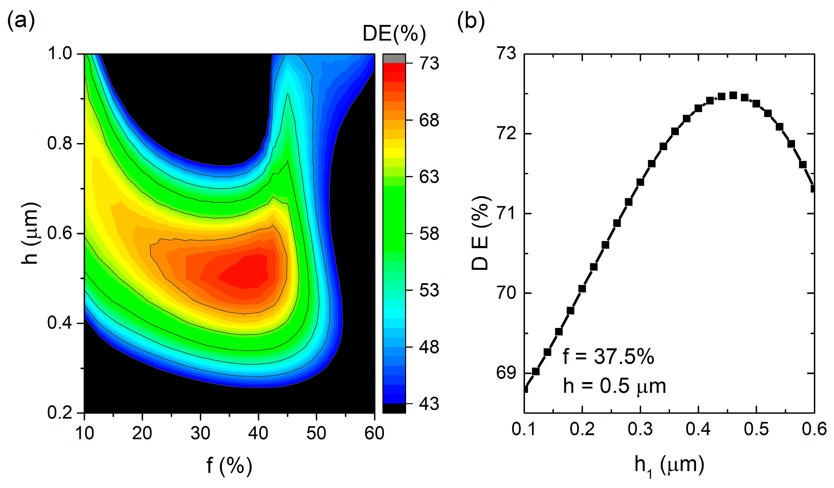
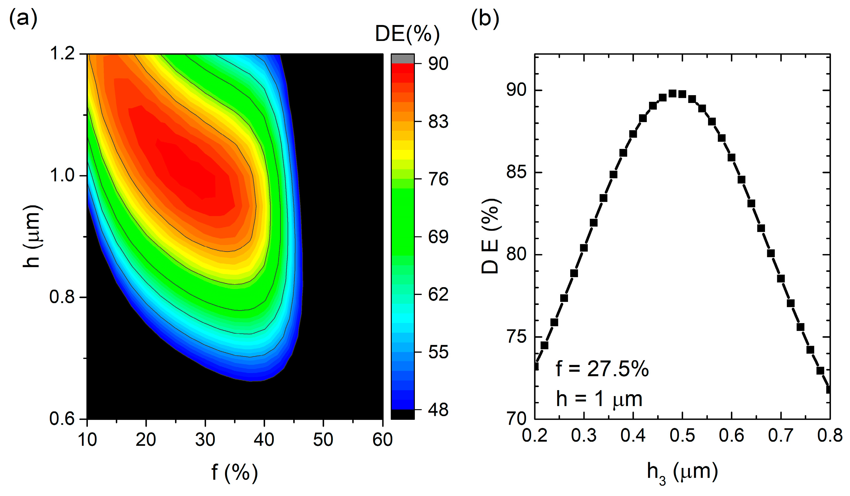
3.2. Increasing Diffraction Efficiency by AR Coatings
4. Discussion
5. Conclusions
Author Contributions
Funding
Institutional Review Board Statement
Informed Consent Statement
Data Availability Statement
Acknowledgments
Conflicts of Interest
Appendix A


References
- Fischer, B.M.; Hoffmann, M.; Helm, H.; Wilk, R.; Rutz, F.; Kleine-Ostmann, T.; Koch, M.; Jepsen, P.U. Terahertz time-domain spectroscopy and imaging of artificial RNA. Opt. Express 2005, 13, 5205–5215. [Google Scholar] [CrossRef] [PubMed] [Green Version]
- Jepsen, P.U.; Cooke, D.G.; Koch, M. Terahertz spectroscopy and Imaging-Modern techniques and applications. Laser Photon. Rev. 2011, 5, 124–166. [Google Scholar] [CrossRef]
- Salén, P.; Basini, M.; Bonetti, S.; Hebling, J.; Krasilnikov, M.; Nikitin, A.Y.; Shamuilov, G.; Tibai, Z.; Zhaunerchyk, V.; Goryashko, V. Matter manipulation with extreme terahertz light: Progress in the enabling THz technology. Phys. Rep. 2019, 836–837, 1–74. [Google Scholar] [CrossRef]
- Manikandan, E.; Princy, S.S.; Sreeja, B.S.; Radha, S. Structure Metallic Surface for Terahertz Plasmonics. Plasmonics 2019, 14, 1311–1319. [Google Scholar] [CrossRef]
- Gupta, D.N. Optical Second-Harmonic Generation of Terahertz Field from n-type InSb Semiconductors. Plasmonics 2020, 16, 419–424. [Google Scholar] [CrossRef]
- Vicario, C.; Jazbinsek, M.; Ovchinnikov, A.V.; Chefonov, O.V.; Ashitkov, S.I.; Agranat, M.B.; Hauri, C.P. High efficiency THz generation in DSTMS, DAST and OH1 pumped by Cr:forsterite laser. Opt. Express 2015, 23, 4573–4580. [Google Scholar] [CrossRef] [Green Version]
- Vicario, C.; Monoszlai, B.; Hauri, C.P. GV/m Single-Cycle Terahertz Fields from a Laser-Driven Large-Size Partitioned Organic Crystal. Phys. Rev. Lett. 2014, 112, 213901. [Google Scholar] [CrossRef] [Green Version]
- Nagai, M.; Tanaka, K.; Ohtake, H.; Bessho, T.; Sugiura, T.; Hirosumi, T.; Yoshida, M. Generation and detection of terahertz radiation by electro-optical process in GaAs using 1.56 mu m fiber laser pulses. Appl. Phys. Lett. 2004, 85, 3974–3976. [Google Scholar] [CrossRef]
- Hebling, J.; Almasi, G.; Kozma, I.Z.; Kuhl, J. Velocity matching by pulse front tilting for large area THz-pulse generation. Opt. Express 2002, 10, 1161–1166. [Google Scholar] [CrossRef] [Green Version]
- Yeh, K.L.; Hoffmann, M.C.; Hebling, J.; Nelson, K.A. Generation of 10μJ ultrashort terahertz pulses by optical rectification. Appl. Phys. Lett. 2007, 90, 171121. [Google Scholar] [CrossRef]
- Zhang, B.; Ma, Z.; Ma, J.; Wu, X.; Ouyang, C.; Kong, D.; Hong, T.; Wang, X.; Yang, P.; Chen, L.; et al. 1.4-mJ High Energy Terahertz Radiation from Lithium Niobates. Laser Photon. Rev. 2021, 15, 2000295. [Google Scholar] [CrossRef]
- Stepanov, A.G.; Hebling, J.; Kuhl, J. Efficient generation of subpicosecond terahertz radiation by phase-matched optical rectification using ultrashort laser pulses with tilted pulse fronts. Appl. Phys. Lett. 2003, 83, 3000–3002. [Google Scholar] [CrossRef]
- Palfalvi, L.; Fülöp, J.A.; Almási, G.; Hebling, J. Novel setups for extremely high power single-cycle terahertz pulse generation by optical rectification. Appl. Phys. Lett. 2008, 92, 171107. [Google Scholar] [CrossRef]
- Nagashima, K.; Kosuge, A. Design of Rectangular Transmission Gratings Fabricated in LiNbO3for High-Power Terahertz-Wave Generation. Jpn. J. Appl. Phys. 2010, 49, 122504. [Google Scholar] [CrossRef]
- Ollmann, Z.; Hebling, J.; Almási, G. Design of a contact grating setup for mJ-energy THz pulse generation by optical rectification. Appl. Phys. B-Lasers O 2012, 108, 821–826. [Google Scholar] [CrossRef]
- Tsubouchi, M.; Nagashima, K.; Yoshida, F.; Ochi, Y.; Maruyama, M. Contact grating device with Fabry–Perot resonator for effective terahertz light generation. J. Opt. Lett. 2014, 39, 5439–5442. [Google Scholar] [CrossRef] [PubMed]
- Hoffmann, M.C.; Yeh, K.L.; Hebling, J.; Nelson, K.A. Efficient terahertz generation by optical rectification at 1035 nm. Opt. Express 2007, 15, 11706–11713. [Google Scholar] [CrossRef]
- Hebling, J.; Yeh, K.L.; Hoffmann, M.C.; Bartal, B.; Nelson, K.A. Generation of high-power terahertz pulses by tilted-pulse-front excitation and their application possibilities. J. Opt. Soc. Am. B 2008, 25, B6–B19. [Google Scholar] [CrossRef]
- Blanchard, F.; Schmidt, B.E.; Ropagnol, X.; Thiré, N.; Ozaki, T.; Morandotti, R.; Cooke, D.G.; Légaré, F. Terahertz pulse generation from bulk GaAs by a tilted-pulse-front excitation at 1.8 mu m. Appl. Phys. Lett. 2014, 105, 241106. [Google Scholar] [CrossRef]
- Vodopyanov, K.L. Optical THz-wave generation with periodically-inverted GaAs. Laser Photon. Rev. 2008, 2, 11–25. [Google Scholar] [CrossRef]
- Ollmann, Z.; Fülöp, J.A.; Hebling, J.; Almási, G. Design of a high-energy terahertz pulse source based on ZnTe contact grating. Opt. Commun. 2014, 315, 159–163. [Google Scholar] [CrossRef]
- Bakunov, M.I.; Bodrov, S.B. Terahertz generation with tilted-front laser pulses in a contact-grating scheme. J. Opt. Soc. Am. B Opt. Phys. 2014, 31, 2549–2557. [Google Scholar] [CrossRef]
- Fülöp, J.A.; Polónyi, G.; Monoszlai, B.; Andriukaitis, G.; Balciunas, T.; Pugzlys, A.; Arthur, G.; Baltuska, A.; Hebling, J. Highly efficient scalable monolithic semiconductor terahertz pulse source. Optica 2016, 3, 1075–1078. [Google Scholar] [CrossRef] [Green Version]
- Polonyi, G.; Mechler, M.I.; Hebling, J.; Fulop, J.A. Prospects of Semiconductor Terahertz Pulse Sources. IEEE J. Sel. Top. Quantum Electron. 2017, 23, 25–29. [Google Scholar] [CrossRef] [Green Version]
- Cui, W.; Awan, K.M.; Huber, R.; Dolgaleva, K.; Ménard, J.M. Broadband and High-Sensitivity Time-Resolved THz System Using Grating-Assisted Tilted-Pulse-Front Phase Matching. Adv. Opt. Mater. 2022, 10, 2101136. [Google Scholar] [CrossRef]
- Bashirpour, M.; Cui, W.; Gamouras, A.; Ménard, J.M. Scalable Fabrication of Nanogratings on GaP for Efficient Diffraction of Near-Infrared Pulses and Enhanced Terahertz Generation by Optical Rectification. Crystals 2022, 12, 684. [Google Scholar] [CrossRef]
- Mbithi, N.M.; Tóth, G.; Tibai, Z.; Benabdelghani, I.; Nasi, L.; Krizsán, G.; Hebling, J.; Polonyi, G. Investigation of terahertz pulse generation in semiconductors pumped at long infrared wavelengths. J. Opt. Soc. Am. B 2022, Submitted. [Google Scholar]
- Wei, J.; Murray, J.M.; Barnes, J.O.; Krein, D.M.; Schunemann, P.G.; Guha, S. Temperature dependent Sellmeier equation for the refractive index of GaP. Opt. Mater. Express 2018, 8, 485–490. [Google Scholar] [CrossRef]
- Parsons, D.F.; Coleman, P.D. Far Infrared Optical Constants of Gallium Phosphide. Appl. Opt. 1971, 10, 1683_1681–1685. [Google Scholar] [CrossRef]
- Kachare, A.H.; Spitzer, W.G.; Fredrickson, J.E. Refractive index of ion-implanted GaAs. J. Appl. Phys. 1976, 47, 4209–4212. [Google Scholar] [CrossRef]
- Palik, E.D. Handbook of Optical Constants of Solids; Academic Press: Cambridge, MA, USA, 1998; Volume 3. [Google Scholar]
- Nguyen, H.T.; Shore, B.W.; Bryan, S.J.; Britten, J.A.; Boyd, R.D.; Perry, M.D. High-efficiency fused-silica transmission gratings. Opt. Lett. 1997, 22, 142–144. [Google Scholar] [CrossRef] [PubMed]
- Krizsán, G.; Tibai, Z.; Almási, G.; Tóth, G.; Pálfalvi, L.; Hebling, J. New Generation Terahertz Pulse Sources Utilizing Volume Phase Holographic Gratings. In Proceedings of the High Intensity Lasers and High Field Phenomena, Budapest, Hungary, 21–25 March 2022; p. HF3B.6. [Google Scholar] [CrossRef]
- Zimmerman, W.B. Multiphysics Modeling with Finite Element Methods; World Scientific Publishing Co. Pte. Ltd.: Singapore, 2006; Volume 18. [Google Scholar]
- Harvey, J.E.; Pfisterer, R.N. Understanding diffraction grating behavior: Including conical diffraction and Rayleigh anomalies from transmission gratings. Opt. Eng. 2019, 58, 087105. [Google Scholar] [CrossRef]
- Clausnitzer, T.; Limpert, J.; Zöllner, K.; Zellmer, H.; Fuchs, H.J.; Kley, E.B.; Tünnermann, A.; Jupé, M.; Ristau, D. Highly efficient transmission gratings in fused silica for chirped-pulse amplification systems. Appl. Opt. 2003, 42, 6934–6938. [Google Scholar] [CrossRef] [PubMed]
- Clausnitzer, T.; Kämpfe, T.; Kley, E.B.; Tünnermann, A.; Peschel, U.; Tishchenko, A.V.; Parriaux, O. An intelligible explanation of highly-efficient diffraction in deep dielectric rectangular transmission gratings. Opt. Express 2005, 13, 10448–10456. [Google Scholar] [CrossRef] [PubMed]


| Material | ARC | n | f (%) | h (nm) | DE(%) | Optimized DE(%) |
|---|---|---|---|---|---|---|
| GaP | − | − | 42 | 430 | 74.2 | − |
| (SiO2) | 1.44 | 42.5 | 400 | = 360 nm) | = 280 nm) | |
| (Al2O3) | 1.73 | 37.5 | 350 | = 350 nm) | = 260 nm) | |
| ) | 1.74 | 30 | 490 | = 300 nm) | = 320 nm) | |
| (NOA) | 1.64 | 32.5 | 750 | = 315 nm) | = 300 nm) | |
| GaAs | − | − | 39 | 540 | 69.0 | − |
| (SiO2) | 1.42 | 37.5 | 500 | = 530 nm) | = 460 nm) | |
| ) | 1.83 | 31 | 620 | = 410 nm) | = 440 nm) | |
| (NOA) | 1.62 | 27.5 | 1000 | = 460 nm) | = 460 nm) |
Publisher’s Note: MDPI stays neutral with regard to jurisdictional claims in published maps and institutional affiliations. |
© 2022 by the authors. Licensee MDPI, Basel, Switzerland. This article is an open access article distributed under the terms and conditions of the Creative Commons Attribution (CC BY) license (https://creativecommons.org/licenses/by/4.0/).
Share and Cite
Tibai, Z.; Mbithi, N.M.; Almási, G.; Fülöp, J.A.; Hebling, J. Design of Semiconductor Contact Grating Terahertz Source with Enhanced Diffraction Efficiency. Crystals 2022, 12, 1173. https://doi.org/10.3390/cryst12081173
Tibai Z, Mbithi NM, Almási G, Fülöp JA, Hebling J. Design of Semiconductor Contact Grating Terahertz Source with Enhanced Diffraction Efficiency. Crystals. 2022; 12(8):1173. https://doi.org/10.3390/cryst12081173
Chicago/Turabian StyleTibai, Zoltán, Nelson M. Mbithi, Gábor Almási, József A. Fülöp, and János Hebling. 2022. "Design of Semiconductor Contact Grating Terahertz Source with Enhanced Diffraction Efficiency" Crystals 12, no. 8: 1173. https://doi.org/10.3390/cryst12081173