Article

A Mesoporous Silica Nanoparticle-Doped Photo-Alignment Layer and Liquid Crystal Layer for Optimizing the Rewriting Speed and the Response Time of Optically Driving Liquid Crystal Displays

College of Information Science and Technology, Donghua University, Shanghai 201620, China
*
Author to whom correspondence should be addressed.
Crystals 2022, 12(8), 1088; https://doi.org/10.3390/cryst12081088
Submission received: 11 July 2022 / Revised: 26 July 2022 / Accepted: 1 August 2022 / Published: 4 August 2022
(This article belongs to the Special Issue Liquid Crystals and Their Advanced Applications)

Abstract

:
Optically driving liquid crystal displays (ODLCDs) are widely applied in display and optical devices due to their long axis of liquid crystal (LC) molecules that can be tuned by a photo-alignment layer under exposure polarized light. However, their use remains challenging due to their long rewriting time and response time. In this work, the rewriting time and the response time of an ODLCD depending on mesoporous silica nanoparticles (MSNs) doped in azo-dye (SD1) and LC 5CB were studied. Among the different concentration ratios of SD1-MSNs (1-0 to 1-0.1), a ratio of 1-0.07 was optimal, decreasing the rewriting time by 40 s (from 69.1 to 29.6 s). Meanwhile, the response time was improved 10 times with MSNs doped into 5CB.

1. Introduction

Liquid crystal (LC) is a mesophase between crystalline solids and isotropic liquids. It is a functional material with the fluidity of ordinary liquids and anisotropy of crystalline solids [1,2]. Liquid crystal display (LCD) technology has developed enormously over the past 50 years. It is already dominating many display markets such as phone products, notebook computer displays, and desktop monitors. Furthermore, LC also found a place in digital data storage, holography, color thermometers, smart windows, optical and biological sensors, and GHz and THz devices [3,4,5,6,7,8,9,10].
The alignment of LC molecules is an important factor in determining the electro-optic properties of LCDs. The conventional alignment method of LCD is the universally rubbing method due to its low cost, simplicity, mature technology, and large-area fabrication [11,12]. However, rubbing technology may cause electrostatic charges and impurities as well as mechanical damage to the surface [13]. In recent years, new non-contact technologies, for example, photo-alignment have been developed to break through the limitation of the rubbing method and fulfill production requirements [14,15]. Photo-alignment technology is known for its alignment characteristics with high anchoring energy and flexibility, which has been widely used for LCDs and LC polymers (LCPs) [16,17]. Compared to the rubbing method, photo-alignment technology provides better tunability and precise control at the micro-domain.
Optically driving liquid crystal displays (ODLCDs) have attracted the interest of many researchers because of their advantages of rewriting and ultra-low consumption [18,19,20,21]. There are two different types of ODLCD alignment layers, a rubbing alignment layer (optical passive, OP) and a photo-alignment layer (optical active, OA). The OA layer (azo-dye, SD1) is sensitive to linearly polarized incident light at a wavelength of 450 nm, and the easy axis of LC molecules are tuned under different polarization directions of blue light. An ideal ODLCD is one that has a high rewriting speed. L. Wang et al. demonstrated that the rewriting speed is increased about four times (from 25 s to 7 s) using an electric field [22]. Jiatong Sun et al. experimentally showed that the rewriting time could be decreased to 6 s with good repeatability by filling LC in atmospheric conditions. Increasing the speed of spin-coating, the rewriting time could also be reduced [23]. Vladimir Chigrinov et al. found that by increasing the operating temperature of the ODLCD to around the LC clearing point, the rewriting time of LC N4 can be increased around 26 times [24].
Meanwhile, a lower response time plays an important role in LCD. The dispersion of nanomaterials as an active-matrix component to optimize the response time of LCD is regarded as an economical and quick method, e.g., nanorods [25,26], quantum dots (QDs) [27], and nanoparticles [28]. Mesoporous silica nanoparticles (MSNs) have been demonstrated for a variety of applications because of their biocompatibility [29], facile synthesis protocols [30], possibilities for modifications of particle and pore sizes and morphologies [31], and high surface area and thermal stability [32]. Thus, functional MSNs dispersed in LCs might enhance the electro-optic performance of LCD devices.
In this work, we demonstrate a novel technology for optimizing the rewriting speed and response time of ODLCD via doping MSNs into the photo-alignment layer (SD1) and LC 5CB. By doping MSNs into the SD1 layer, the rewriting speed can be increased around 2.3 times. Meanwhile, the response time can be gradually decreased to 3.73 ms from 37.46 ms with MSNs doped into 5CB. The MSNs doped photo-alignment layer and 5CB are significantly beneficial to the ODLCD.

2. Materials and Methods

2.1. Materials

Dimethylformamide (DMF) was purchased from Sigma-Aldrich (St. Louis, MO, USA). Cetyltrimethylammonium bromide (CTAB) was obtained from Tokyo Chemical Industry Co., Ltd. (TCI, Shanghai, China). Photosensitive SD1 was obtained from Dainippon Ink and Chemicals Co., Ltd. (DIC Corp., Tokyo, Japan). Tetraethyl orthosilicate (TEOS), n-hexane, concentrated ammonia-water (28 wt%), hydrochloric acid (HCl), and ethanol were obtained from Sinopharm Chemical Reagent Co., Ltd. (Beijing, China). Polyimide (PI, DL-2193) was purchased from Yesheng Co., Ltd. (Hebei, China). LC 5CB was obtained from Merck Co., Ltd. (Kenilworth, NJ, USA). Deionized water was used for all experiments.

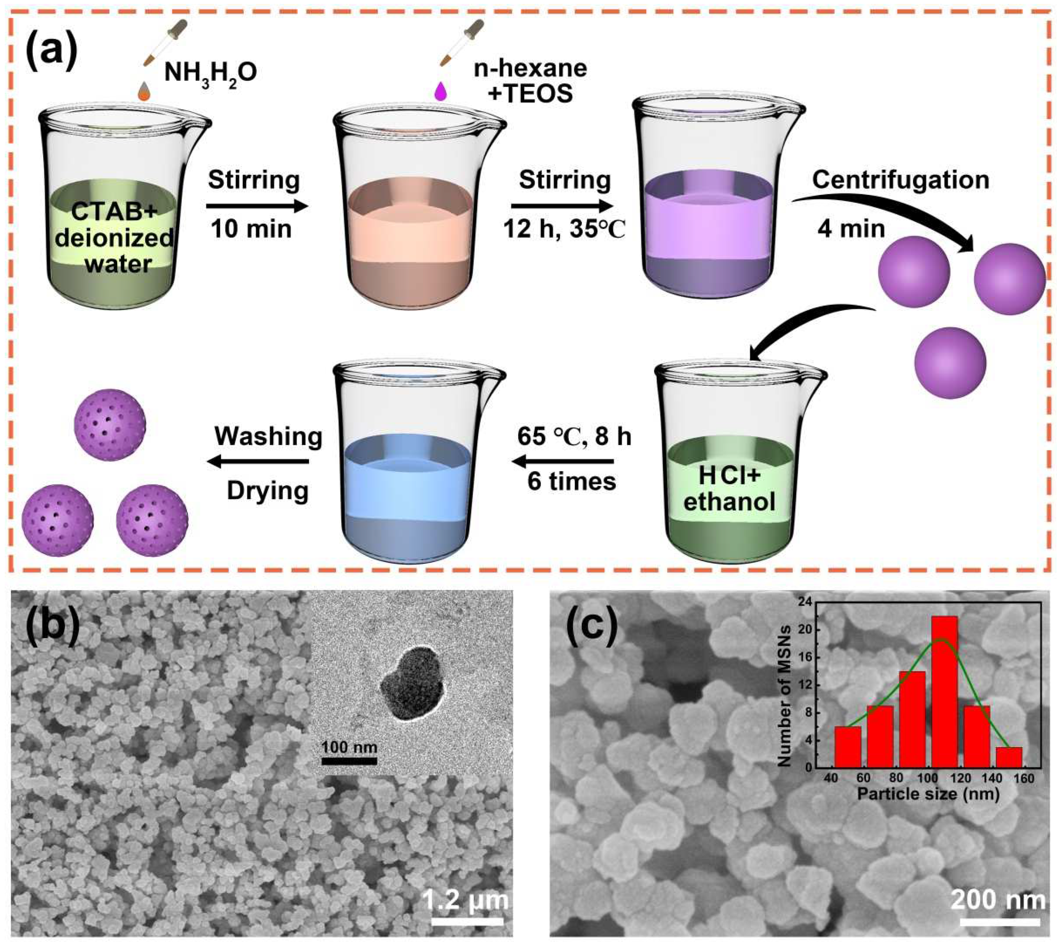
2.2. Synthesis of MSNs

MSNs were synthesized by a similar Stöber process in an alkali ethanol/water solution [33]. Briefly, CTAB (1.0 g) was added to deionized water (160 mL) under stirring. After that, concentrated ammonia-water (3.0 mL, 28 wt.%) was added and stirred for 10 min. Then, a mixture of TEOS (5 mL) and n-hexane (20 mL) was dropped into the solution and stirred continuously for 30 min. A homogeneous milky colloidal solution was gradually formed under continuous stirring (200 rpm, 35 °C). The product was collected by centrifugation (9000 rpm, 4 min) after stirring for 12 h, and the product was washed with deionized water and ethanol. The collected solid sample was then solvent extracted to remove the CTAB templates by dispersing it in a mixture of HCl (0.7 mL, 37%) and ethanol (100 mL) at 65 °C for 8 h. The solvent extraction was repeated 6 times, and the sample was collected by centrifugation, washed with ethanol 6 times, and finally dried overnight under vacuum. MSNs were thus obtained.

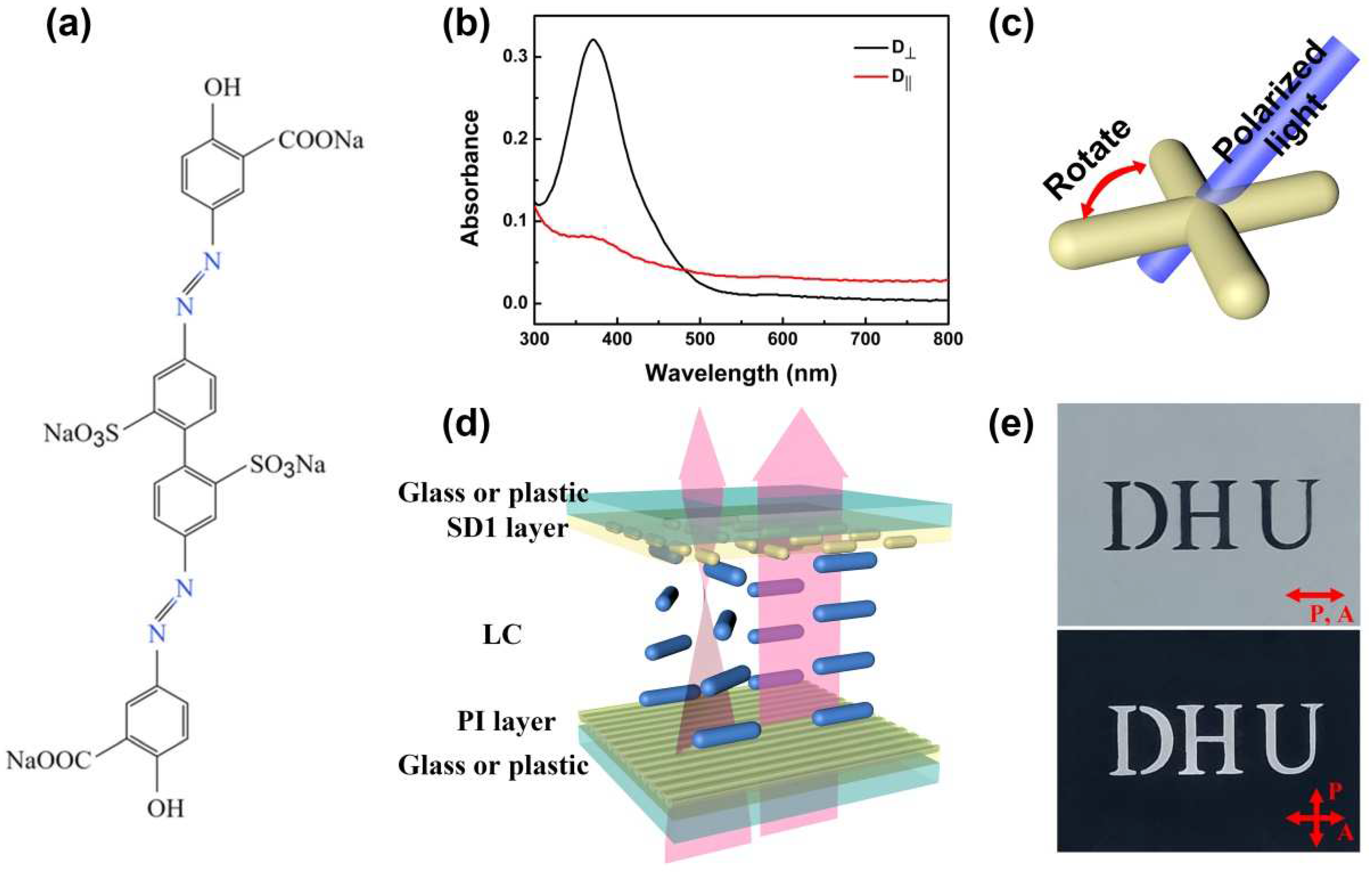
2.3. Preparation of ODLCD

The cell of ODLCD consisted of two glass substrates, a photo-alignment layer, and a polyimide (PI) rubbing layer. The UV light-sensitive material SD1 was added to DMF with a concentration of 0.5 wt.%. A drop of solution (pure SD1 and different concentration SD1-MSNs) was spin-coated on a glass substrate at 3000 rpm for 30 s and then heated for 30 min to remove the excess solvent. The SD1 layer was irradiated under a polarized blue laser with a wavelength of 450 nm. A PI (2 wt.%) solution was dropped onto the substrate, and then the substrate was spin-coated at a speed of 3000 rpm for 100 s. The PI-coated substrate was then heated on a hotplate at 230 °C for 60 min, then naturally cooled to room temperature. Next, the PI substrate was rubbed with a velvet cloth. The cell gap of the LC cells was fixed by spacers of 10 μm. The commercial nematic LC 5CB and different concentrations of 5CB-MSNs were used in the experiment. Then, the desired part of the ODLCD sample was blocked with a photo mask and exposed under the same 450 nm blue LED light; its polarization plane was orthogonal to the prearranged polarization direction to display the desired pattern.

2.4. Characterization

The surface morphologies of MSNs and SD1-MSNs films were characterized by scanning electron microscopy (SEM, S-4800; Hitachi, Tokyo, Japan) and transmission electron microscopy (TEM, Talos F200S; Thermo Fisher Scientific, Waltham, MA, USA). The rewriting time was recorded by optical devices. The absorption spectra of the SD1 layer after linearly polarized UV light (450 nm) irradiation was measured using UV-visible-near-infrared spectrophotometry (UV-3600; Shimadzu, Kyoto, Japan). The response time of ODLCD was measured by an LC device parameter tester (ALCTE-EO1S, ALCT- 4.60.151123P, Instec, Boulder, CO, USA).

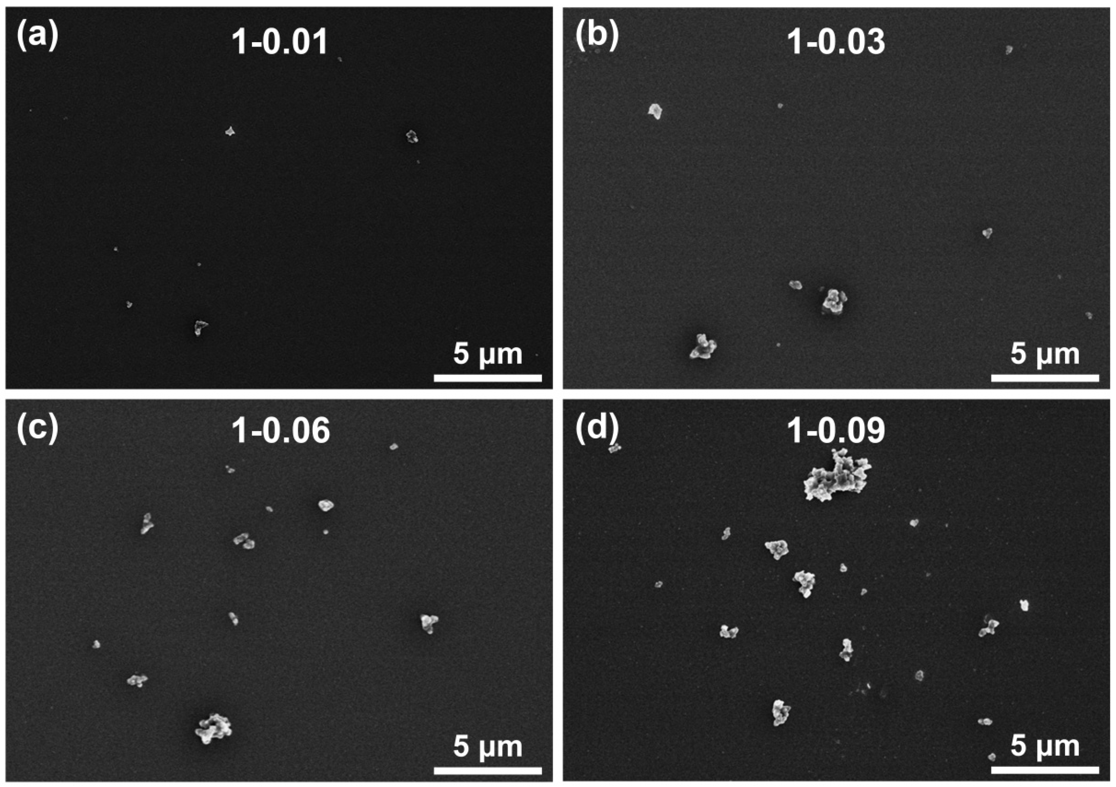
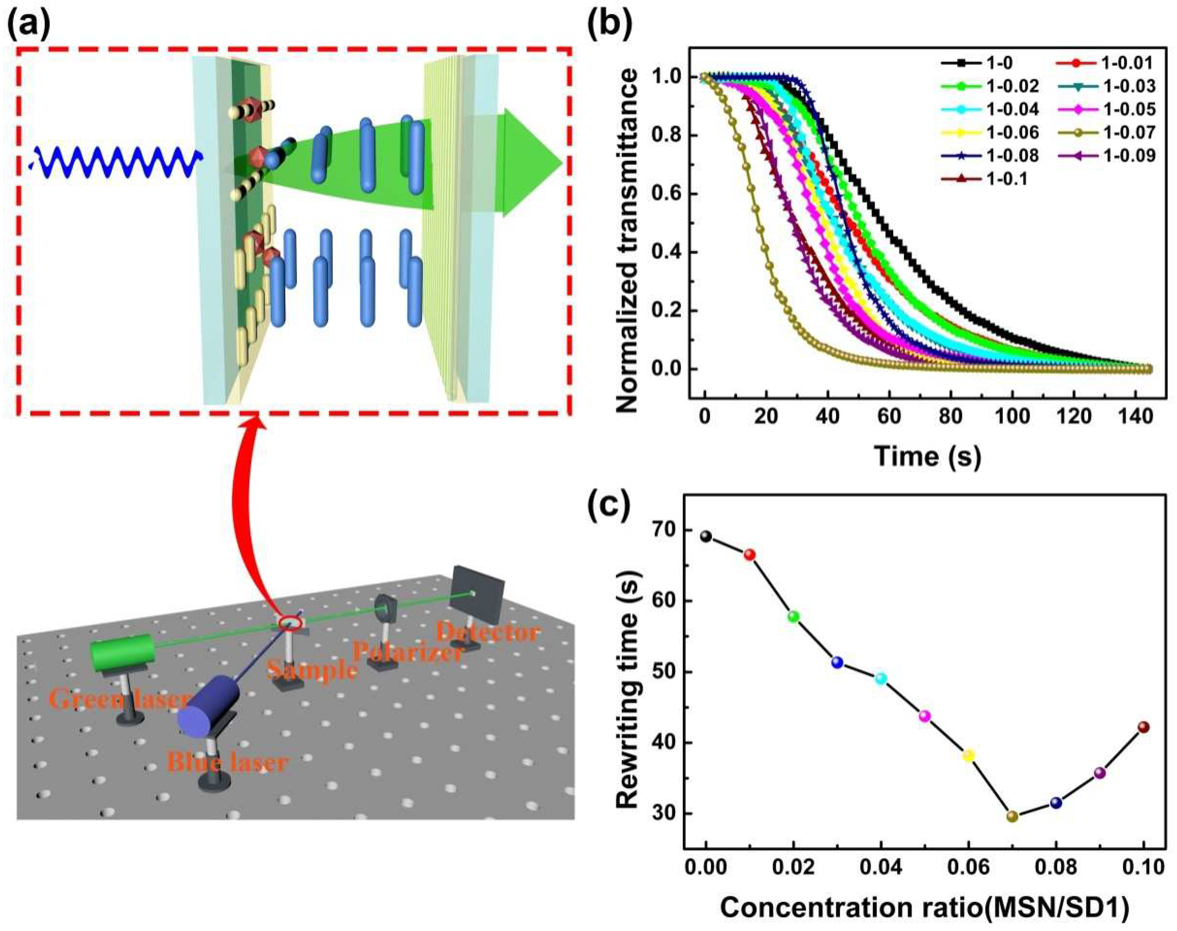
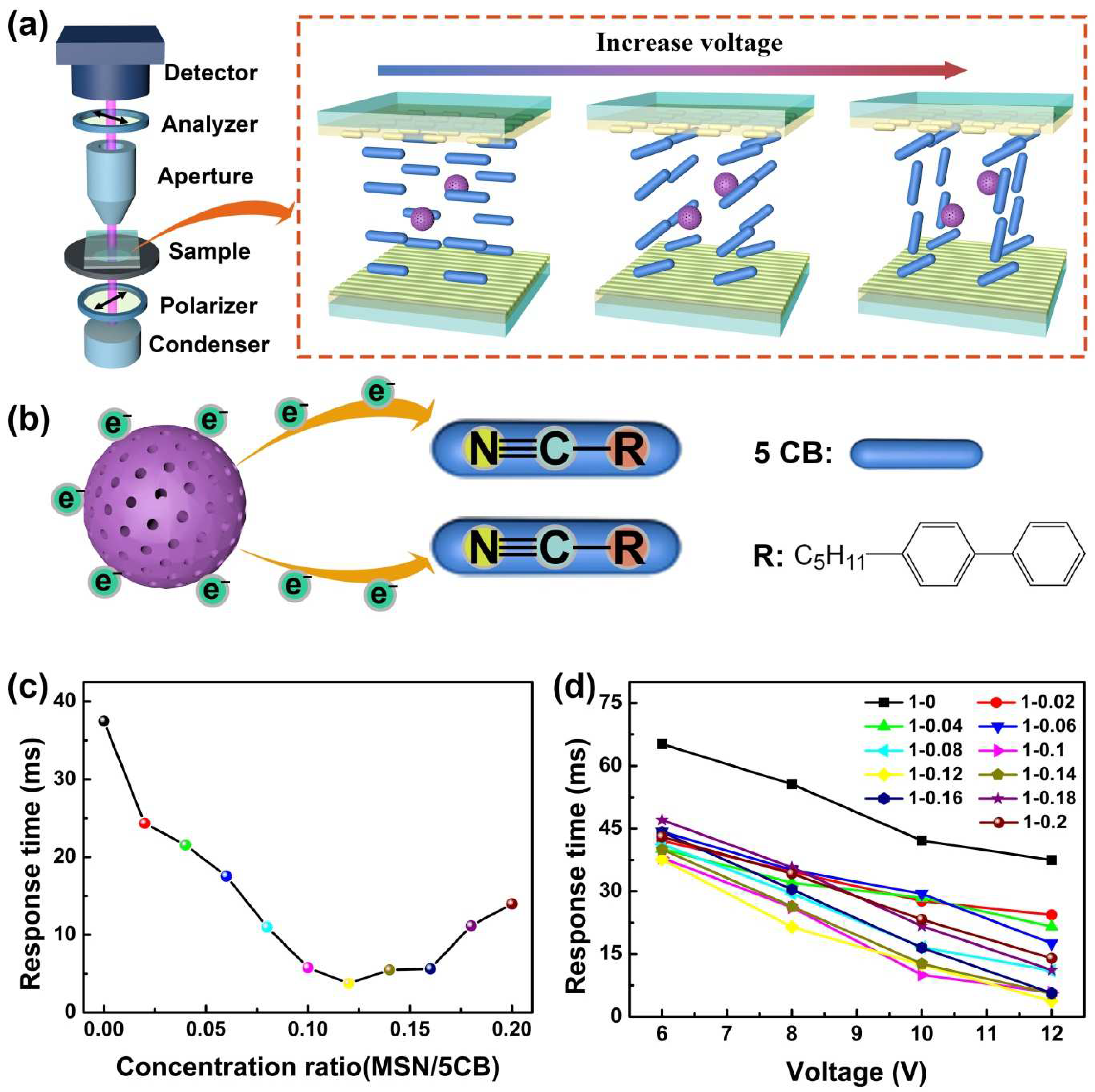
3. Results and Discussion

The MSNs were prepared using a similar Stöber process. The detailed fabrication process is described in the Materials and Methods, and the schematic diagrams are shown in Figure 1a. The silica nanoparticles were grown in a composite solution via a few steps, and then the silica nanoparticles were removed from CTAB templates by redispersing them in a mixture of HCl and ethanol. Finally, the MSNs were fabricated. Figure 1b show a typical SEM image of MSNs, from which it can be observed that the MSNs are spherosome and have a uniform size. A TEM image of a single MSN is inserted in Figure 1b, indicating the nanoparticle is about 120 nm in diameter. An enlarged SEM image reveals that the nanoparticle diameters of MSNs are mainly in the range of 40–160 nm, as shown in Figure 1c. A histogram of the MSN’s diameter is inserted in Figure 1c, and the average diameter is about 98 nm. MSNs have a rough surface and uniform mesopores, favorable for open pores loaded and released with a molecular level drug or dye.
The molecular chemical structure of SD1 in the experiment is shown in Figure 2a. The long axis of rod-like SD1 molecules can be aligned or changed by irradiation with a linearly polarized UV incident light (450 nm). Figure 2b show the polarized absorption spectra of the SD1 layer after linearly polarized UV light irradiation. The absorption of light with a polarization direction parallel to the direction of the activated light (D||) decreases (red line) while the one with the perpendicular direction (D) increases (black line). The SD1 molecules that have their transition dipole moments parallel to the direction of the polarized light will most probably obtain excess energy, which results in their reorientation from the initial position. For rod-like SD1 molecules, the schematic diagram is shown in Figure 2c. With cylindrical symmetry, the only coordinate will be a polar angle θ, the angle between the molecular absorption oscillator and the direction of the polarization of the activating light. The potential energy is [34,35,36,37]
U = ΦkT
Φ = A 2 cos 2 θ ,   A = I α V M τ k T .
Thus, the potential energy U can be written as
U = 1 2 I α V M τ cos 2 θ
where T is the absolute temperature, k is the Boltzmann’s constant, Φ is the relative potential energy, I is the light power (W/cm2), α is the absorption coefficient (cm−1), VM is the molecular volume, and τ is the relaxation time. Therefore, the energy from the polarized blue light can be absorbed by SD1 molecules, and it is proportional to cos2θ.
The micro-images with different LC alignment modes can be realized by photomasks and multi-step irradiation. The schematic diagram of ODLCD is shown in Figure 2d. The multi-step irradiation area is, therefore, a region of the twisted nematic (TN) model, where the first irradiation area remains a region of planar alignment (PA) and can be distinguished by the analyzer and polarizer. The images with a “DHU” pattern were developed for the ODLCD by the pixels dividing method between the analyzer and polarizer, as shown in Figure 2e. The black (above) and white regions (below) represent the TN domain, and the rest of the regions represent the PA domain.
The surface morphology of different SD1-MSN composites on glass substrates was characterized using SEM, as shown in Figure 3, and it was found to closely relate to MSN concentrations. In Figure 3a, it could be seen that the 1-0.01 MSNs nanoparticles with small size were homogeneously distributed on the substrate. However, as the concentration was increased from 1-0.03 to 1-0.06 to 1-0.09, more and larger MSNs nanoparticles appeared (Figure 3b–d), indicating that some particles are stacked together.
The rewriting time of the ODLCD with an MSN-doped SD1 layer was tested and is shown in Figure 4. The testing schematic is shown in Figure 4a: the SD1 layer was irradiated for the first time by 450 nm polarization light, and the LC cell was developed using the PA model. A blue laser with a wavelength of 450 nm was applied for writing, erasing, and rewriting the LC alignment model for the ODLCD samples. The intensity of the green laser (532 nm) through the LC cell and polarizer was detected by a detector. When the blue laser irradiates the SD1 layer (polarization direction parallel to the long axis of SD1 molecule), the SD1 molecules will be changed by 90 degrees. The irradiation region will also change from a PA to TN domain, and the polarization axis of the green laser will be changed. The varying intensity of the green laser through the polarizer can be recorded by a detector. Figure 4b show the curves of normalized transmittance dependence irradiation time for different concentrations of SD1-MSN. The curves tended to increase with increasing MSN concentrations. The rewriting time is the time taken from the transmission reaching from 90% to 10% under a blue polarization light. The rewriting time of all samples is shown in Figure 4c. When the MSN concentration increased from 1-0 to 1-0.07, the rewriting time decreased to 29.6 s from 69.1 s gradually. When the MSN concentration exceeded 1-0.07, the rewriting time increased slightly due to the aggregation of MSNs. The aggregation of MSNs damaged the reorientation of SD1 and disturbed the nearby LC alignment, which caused the longer rewriting time. The rewriting time of 1-0.1 was still less than that of pure SD1. Compared to pure SD1, 2.3 times decrease in rewriting time was obtained by the MSN/SD1 composite. A comparison of the rewriting times of the MSNs doped SD1 layer and several reported methods are presented in Table 1. The decreasing rewriting time is mainly due to the trapping and neutralizing of mobile ions by MSN nanoparticles in the SD1-MSNs composite that enhanced electron transport, leading to faster reconversion of the SD1 molecule.
Since the synthesized MSNs provided a promising platform to develop novel electro-optic devices, the response time of MSNs doped in 5CB was investigated, as shown in Figure 5. Figure 5a show the schematic diagrams of testing and LC molecules at different voltages. When the voltage increased, the angle between the LC director n and the substrate increased gradually, which influenced the intensity of polarized light. A speculative mechanism was proposed to explain the enhancement of the electro-optic properties of the LCs in the presence of MSNs. The sample of MSNs was measured to have a negative zeta potential because the numerous silanol groups provide a negatively charged surface for the MSNs [38], indicating the charges transformation process from the MSNs to LC molecules. The schematic diagram is shown in Figure 5b. The charge transferred to the LC molecules from the MSNs increases the electron density of the LC molecules, redistributes the electron cloud, significantly increases the molecular dipole moment, and enhances the electro-optic activity. Figure 5c show the response time (rising time, ton) of different concentrations of MSNs under 20 V. Here, ton is the time taken from the transmission reaching from 90% to 10% under a voltage. The MSNs concentration increased from 1-0 to 1-0.16, ton decreased gradually to 3.73 ms from 37.46 ms, and then increased when the concentration exceeded 1-0.16 due to the aggregation of MSNs. The aggregation of MSNs disturb the nearby LC alignment, which causes the longer ton of the LC molecules from parallel to vertical to the substrate, compared to pure LC molecules. The ton variation curves of pure 5CB and MSN-5CB composite as a function of the applied electric field are shown in Figure 5d. The ton of pure 5CB, as well as its MSN-5CB composite, decrease with increasing applied electric field. Similar to a 12 V electric field, the ton of 1-0.12 is the smallest of the other concentration ratios.

4. Conclusions

In summary, we developed a facile strategy to synthesize MSNs with shape-regularity and high uniformity, as well as excellent rewriting time and response time of SD1 and 5CB with MSNs doped for the ODLCD. As a result, the minimum rewriting time was 29.6 s when the SD1-MSNs concentration was 1-0.07. In addition to the excellent rewriting speed, the LC 5CB doped with MSNs of different doping concentrations possessed a lower response time. Our general approach of MSNs with SD1 and LC offers fabrication possibilities for ODLCD devices with improved rewriting speed and switching speed.

Author Contributions

Conceptualization, J.S. (Jingxin Sang) and Y.L.; methodology, J.S. (Jianhua Shang) and J.S. (Jiatong Sun); investigation, J.S. (Jianhua Shang); writing—original draft preparation, J.S. (Jingxin Sang) and Y.L.; writing—review and editing, J.S. (Jiatong Sun), J.S. (Jianhua Shang) and S.Z.; funding acquisition, J.S. (Jiatong Sun) and J.S. (Jingxin Sang). All authors have read and agreed to the published version of the manuscript.

Funding

This research was funded by the Fundamental Research Funds for Central Universities (DHU Distinguished Young Professor Program) [22D210401], the Songjiang Science and Technology Commission project [19SJKJGG82], the National Natural Science Foundation of China (NSFC) [61805035], the China Scholarship Council (CSC) [202106630045], and the Fundamental Research Funds for the Central Universities and Graduate Student Innovation Fund of Donghua University [CUSF-DH-D-2022075].

Institutional Review Board Statement

Not applicable.

Informed Consent Statement

Not applicable.

Data Availability Statement

Data presented in this article are available upon request from the corresponding author.

Acknowledgments

The authors gratefully thank Jiatong Sun for the provision of funding for this study.

Conflicts of Interest

The authors declare no conflict of interest.

References

  1. De Gennes, P.G.; Prost, J. The Physics of Liquid Crystals; Oxford University Press: New York, NY, USA, 1993. [Google Scholar]
  2. Sang, J.; Zhang, J.; Feng, H.; Sun, J.; Shang, J.; Zhang, Y.; Zhao, S.; Neyts, K.; Chigrinov, V. Flexible and Transferable Silver Nanowire Liquid Crystal Polymer Film Obtained via Photo-Alignment Programming. Adv. Opt. Mater. 2022, 2200950. [Google Scholar] [CrossRef]
  3. Eskalen, H.; Özğan, Ş.; ALVER, Ü.; Kerli, S. Electro-Optical Properties of Liquid Crystals Composite with Zinc Oxide Nanoparticles. Acta Phys. Pol. A 2015, 127, 756–760. [Google Scholar] [CrossRef]
  4. Tejaswi, M.; Pardhasaradhi, P.; Madhav, B.; Rao, M.; Krishna Mohan, N.; Manepalli, R. Spectroscopic studies on liquid crystalline n-hexyloxy-cyanobiphenyl with dispersed citrate-capped gold nanoparticles in visible region. Liq. Cryst. 2020, 47, 918–938. [Google Scholar] [CrossRef]
  5. Karabuğa, H.; Mert, H.H.; Karanlık, G.; Ocak, H. Synthesis and Characterization of Bent-Core Liquid Crystal/Modified γ-Al2O3 Nanocomposites. Chem. Select 2019, 4, 8983–8988. [Google Scholar]
  6. Eskalen, H. Influence of carbon quantum dots on electro–optical performance of nematic liquid crystal. Appl. Phys. A 2020, 126, 708. [Google Scholar] [CrossRef]
  7. Sang, J.; Zhu, W.; Feng, Y.; Liu, Y.; Shang, J.; Sun, J.; Guo, L.; Zhang, Y.; Zhao, S.; Chigrinov, V. Smart Windows with a VO2 Thin Film as a Conductive Layer for Efficient and Independent Dual-Band Modulation. ACS Appl. Electron. Mater. 2021, 3, 4882–4890. [Google Scholar] [CrossRef]
  8. Olifierczuk, M.; Kowerdziej, R.; Jaroszewicz, L.; Czerwinski, M.; Parka, J. Numerical analysis of THz metamaterial with high birefringence liquid crystal. Liq. Cryst. 2012, 39, 739–744. [Google Scholar] [CrossRef]
  9. Polat, E.; Reese, R.; Jost, M.; Schuster, C.; Nickel, M.; Jakoby, R.; Maune, H. Tunable liquid crystal filter in nonradiative dielectric waveguide technology at 60 GHz. IEEE Microw. Wirel. Compon. Lett. 2019, 29, 44–46. [Google Scholar] [CrossRef]
  10. Jakoby, R.; Gaebler, A.; Weickhmann, C. Microwave liquid crystal enabling technology for electronically steerable antennas in SATCOM and 5G millimeter-wave systems. Crystals 2020, 10, 514. [Google Scholar] [CrossRef]
  11. Liu, Y.; Sang, J.; Liu, H.; Xu, H.; Zhao, S.; Sun, J.; Lee, J.H.; Jeong, H.-C.; Seo, D.-S. Decreasing the residual DC voltage by neutralizing the charged mobile ions in liquid crystals. Crystals 2019, 9, 181. [Google Scholar] [CrossRef] [Green Version]
  12. Chen, P.; Wei, B.Y.; Hu, W.; Lu, Y.Q. Liquid-crystal-mediated geometric phase: From transmissive to broadband reflective planar optics. Adv. Mater. 2020, 32, 1903665. [Google Scholar] [CrossRef] [PubMed]
  13. Chigrinov, V.G. Photoaligning and photopatterning—A new challenge in liquid crystal photonics. Crystals 2013, 3, 149–162. [Google Scholar] [CrossRef] [Green Version]
  14. Murauski, A.; Chigrinov, V.G.; Li, X.; Kwok, H.S. Optically rewriteable LC display with a high contrast and long life time. In IDW/AD’05-Proceedings of the 12th International Display Workshops in Conjunction with Asia Display 2005; The Institute of Image Information and Television Engineers: Tokyo, Japan, 2005; p. 131. [Google Scholar]
  15. Chigrinov, V.G.; Belyaev, V.V.; Kozenkov, V.M.; Chausov, D.N.; Margaryan, H.L.; Hakobyan, N.H.; Tabiryan, N.V. Azodyes for liquid crystal photoalignment in displays and diffraction optical elements. In Proceedings of the Emerging Liquid Crystal Technologies XVII, SPIE, San Francisco, CA, USA, 26 July 2022; pp. 26–36. [Google Scholar]
  16. Sang, J.; Han, L.; Liu, M.; Shang, J.; Sun, J.; Guo, L.; Ge, D.; Zhang, Y.; Zhao, S.; Chigrinov, V.G. Dynamic orientation of silver nanowires via photoalignment for liquid crystal display technology. ACS Appl. Nano Mater. 2021, 4, 12937–12942. [Google Scholar] [CrossRef]
  17. Xiong, J.; Yang, Q.; Li, Y.; Wu, S.-T. Holo-imprinting polarization optics with a reflective liquid crystal hologram template. Light. Sci. Appl. 2022, 11, 1–9. [Google Scholar] [CrossRef] [PubMed]
  18. Sun, J.; Srivastava, A.K.; Zhang, W.; Wang, L.; Chigrinov, V.G.; Kwok, H.S. Optically rewritable 3D liquid crystal displays. Opt. Lett. 2014, 39, 6209–6212. [Google Scholar] [CrossRef]
  19. Zhang, Y.; Sun, J.; Liu, Y.; Shang, J.; Liu, H.; Liu, H.; Gong, X.; Chigrinov, V.; Kowk, H.S. A flexible optically re-writable color liquid crystal display. Appl. Phys. Lett. 2018, 112, 131902. [Google Scholar] [CrossRef]
  20. Du, T.; Fan, F.; Tam, A.M.W.; Sun, J.; Chigrinov, V.G.; Sing Kwok, H. Complex nanoscale-ordered liquid crystal polymer film for high transmittance holographic polarizer. Adv. Mater. 2015, 27, 7191–7195. [Google Scholar] [CrossRef]
  21. Sun, J.; Ren, L.; Deng, K.; Wang, T.; Guo, Q.; Sang, J.; Liu, Y.; Liu, H.; Shang, J.; Chigrinov, V. Greyscale generation for optically driving liquid crystal display. Liq. Cryst. 2019, 46, 1340–1344. [Google Scholar] [CrossRef]
  22. Wang, L.; Sun, J.; Liu, H.; Chigrinov, V.; Kwok, H.S. Increasing the rewriting speed of ORW e-paper by electric field. Liq. Cryst. 2018, 45, 553–560. [Google Scholar] [CrossRef]
  23. Sun, J.; Liu, Y.; Liu, H.; Gong, X.; Chigrinov, V.G. Increasing rewriting speed of optically driving liquid crystal display by process optimisation. Liq. Cryst. 2019, 46, 151–157. [Google Scholar] [CrossRef]
  24. Chigrinov, V.; Sun, J.; Kuznetsov, M.M.; Belyaev, V.; Chausov, D. The Effect of Operating Temperature on the Response Time of Optically Driven Liquid Crystal Displays. Crystals 2020, 10, 626. [Google Scholar] [CrossRef]
  25. Acharya, S.; Kundu, S.; Hill, J.P.; Richards, G.J.; Ariga, K. Nanorod-Driven Orientational Control of Liquid Crystal for Polarization-Tailored Electro-Optic Devices. Adv. Mater. 2009, 21, 989–993. [Google Scholar] [CrossRef]
  26. Kundu, S.; Hill, J.P.; Richards, G.J.; Ariga, K.; Khan, A.H.; Thupakula, U.; Acharya, S. Ultranarrow PbS nanorod-nematic liquid crystal blend for enhanced electro-optic properties. ACS Appl. Mater. Interfaces 2010, 2, 2759–2766. [Google Scholar] [CrossRef]
  27. Lee, W.-K.; Hwang, S.J.; Cho, M.-J.; Park, H.-G.; Han, J.-W.; Song, S.; Jang, J.H.; Seo, D.-S. CIS–ZnS quantum dots for self-aligned liquid crystal molecules with superior electro-optic properties. Nanoscale 2013, 5, 193–199. [Google Scholar] [CrossRef] [PubMed]
  28. SJ, S.; Gupta, R.; Kumar, S.; Manjuladevi, V. Enhanced electro-optical response of nematic liquid crystal doped with functionalised silver nanoparticles in twisted nematic configuration. Liq. Cryst. 2020, 47, 1678–1690. [Google Scholar]
  29. Tang, F.; Li, L.; Chen, D. Mesoporous silica nanoparticles: Synthesis, biocompatibility and drug delivery. Adv. Mater. 2012, 24, 1504–1534. [Google Scholar] [CrossRef] [PubMed]
  30. Wu, S.-H.; Mou, C.-Y.; Lin, H.-P. Synthesis of mesoporous silica nanoparticles. Chem. Soc. Rev. 2013, 42, 3862–3875. [Google Scholar] [CrossRef] [PubMed]
  31. Knežević, N.Ž. Core/shell magnetic mesoporous silica nanoparticles with radially oriented wide mesopores. Process. Appl. Ceram. 2014, 8, 109–112. [Google Scholar] [CrossRef] [Green Version]
  32. Knežević, N.Z.; Ilić, N.A.; Ðokić, V.; Petrović, R.; Janaćković, D.O.E. Mesoporous silica and organosilica nanomaterials as UV-blocking agents. ACS Appl. Mater. Interfaces 2018, 10, 20231–20236. [Google Scholar] [CrossRef] [PubMed]
  33. Stöber, W.; Fink, A.; Bohn, E. Controlled growth of monodisperse silica spheres in the micron size range. J. Colloid Interface Sci. 1968, 26, 62–69. [Google Scholar] [CrossRef]
  34. Ma, Y.; Xin, S.J.; Liu, X.; Liu, Y.; Sun, J.; Wang, X.; Guo, Q.; Chigrinov, V.G. Colour generation for optically driving liquid crystal display. Liq. Cryst. 2020, 47, 1729–1734. [Google Scholar] [CrossRef]
  35. Chen, P.; Ma, L.L.; Duan, W.; Chen, J.; Ge, S.J.; Zhu, Z.H.; Tang, M.J.; Xu, R.; Gao, W.; Li, T. Digitalizing self-assembled chiral superstructures for optical vortex processing. Adv. Mater. 2018, 30, 1705865. [Google Scholar] [CrossRef] [PubMed]
  36. Ge, S.; Chen, P.; Shen, Z.; Sun, W.; Wang, X.; Hu, W.; Zhang, Y.; Lu, Y. Terahertz vortex beam generator based on a photopatterned large birefringence liquid crystal. Opt. Express 2017, 25, 12349–12356. [Google Scholar] [CrossRef] [PubMed] [Green Version]
  37. Chigrinov, V.; Pikin, S.; Verevochnikov, A.; Kozenkov, V.; Khazimullin, M.; Ho, J.; Huang, D.D.; Kwok, H.-S. Diffusion model of photoaligning in azo-dye layers. Phys. Rev. E 2004, 69, 061713. [Google Scholar] [CrossRef] [PubMed] [Green Version]
  38. Wang, X.; Zhang, Y.; Luo, W.; Elzatahry, A.A.; Cheng, X.; Alghamdi, A.; Abdullah, A.M.; Deng, Y.; Zhao, D. Synthesis of ordered mesoporous silica with tunable morphologies and pore sizes via a nonpolar solvent-assisted stober method. Chem. Mater. 2016, 28, 2356–2362. [Google Scholar] [CrossRef]
Figure 1. (a) A schematic diagram of the fabrication process for mesoporous silica nanoparticles (MSNs). (b) Scanning electron microscopy (SEM) image of MSNs, with the transmission electron microscopy (TEM) image of a single MSN in the insert. (c) An enlarged SEM image of MSNs. The insets in panel (c) show the statistical diameter distribution profile.
Crystals 12 01088 g001
Figure 2. (a) Chemical structure of SD1. (b) Absorption spectra of SD1 layer after exposure to linearly polarized UV light in the direction parallel (D||) and perpendicular (D) to the activating light polarization accordingly. (c) Schematic diagram of SD1 molecules under linearly polarized UV light. (d) Schematic of ODLCD in which two alignment domains with planar alignment (PA) and twisted nematic (TN) domains. (e) Digital photographs with a “DHU” pattern between the analyzer and polarizer.
Crystals 12 01088 g002
Figure 3. SEM images of the different SD1-MSNs composite films on glass substrates.
Crystals 12 01088 g003
Figure 4. (a) Schematic diagram of ODLCD rewriting time measurement. (b) Normalized transmittance of LC cell with different MSN/SD1 ratios as a function of time. (c) The average rewriting time of 11 different SD1-MSN ratios.
Crystals 12 01088 g004
Figure 5. (a) Schematic diagrams of the electro-optic setup and electrical switching of LCs and MCNs. (b) Schematic diagrams of the charge transformation process between the MSNs and LC molecules. (c) Response time for LC cells doped with different of MSNs concentrations. (d) Response time vs. applied electric field for pure 5CB and MSN/5CB composites.
Crystals 12 01088 g005
Table 1. Comparison of rewriting time of this work and several reported works.
MethodsPre-Optimization Rewriting Time (s)Optimized Rewriting Time (s)Reference
Applying electric field257[22]
Spin-coating time118.7[23]
Filling methods116.5[23]
Operating temperature5.20.2[24]
MSNs doped SD169.129.6This work
Publisher’s Note: MDPI stays neutral with regard to jurisdictional claims in published maps and institutional affiliations.

