Article

A First-Principles Study on the Structural and Carrier Transport Properties of Inorganic Perovskite CsPbI3 under Pressure

1
School of Material Science and Physics, China University of Mining and Technology, Xuzhou 221116, China
2
School of Safety Engineering, China University of Mining and Technology, Xuzhou 221116, China
3
State and Local Joint Engineering Laboratory of Perception Mine, China University of Mining and Technology, Xuzhou 221116, China
4
School of Information and Control Engineering, China University of Mining and Technology, Xuzhou 221116, China
*
Author to whom correspondence should be addressed.
These authors contributed equally to this work.
Crystals 2022, 12(5), 648; https://doi.org/10.3390/cryst12050648
Submission received: 3 April 2022 / Revised: 28 April 2022 / Accepted: 29 April 2022 / Published: 1 May 2022

Abstract

:
Lead halide perovskite has attracted intensive attention for pressure and strain detection. Principally, pressure-induced changes in the structure and resistance of perovskite may bring great potential for developing high-performance piezoresistive pressure sensors. Herein, for the first time, we study the structural changes and the hot carrier cooling process of perovskite CsPbI3 under pressure based on density functional theory and time-dependent density functional theory. The calculation results show that the lattice constant of CsPbI3 linearly decreases and the time and path of the hot carrier cooling process change apparently under pressure. Meanwhile, the pressure will change the transition dipole moment, and the position of the k-point will not affect the optical properties of perovskite. Subsequently, the electrical conductivity enlarges as the pressure increases due to the change in charge density caused by pressure, which will be helpful for its potential application in the pressure sensors.

1. Introduction

The inorganic halide perovskite is emerging as a semiconducting material with superior optoelectronic properties, solution-state synthesis, long carrier diffusion length and lifetime, and high defect tolerance [1,2,3,4,5,6,7]. These properties have been leveraged in solar cells, light-emitting diode, sensors, laser, piezoelectric, detector and catalyst [8,9,10,11,12,13,14]. Notably, the crystallographic lattice constant, optical and electronic properties of perovskite will change with varied pressure, which will further lead to different microscopic and macroscopic electrical properties [15]. Vice versa, the change of optical or electrical properties of perovskite under pressure can be used to obtain the magnitude of pressure, strain and stress, making it suitable to prepare high sensitivity pressure, strain and stress sensors [16,17]. High-performance stress, strain and pressure sensors have been widely used in various fields including health monitoring, robotic hand, earthquake warning and spacecraft [18]. Zhong et al. fabricated the in situ perovskite quantum dots film with distributed Bragg reflectors cavity for constructing an optical pressure sensor; the pressure was measured by using the change of the photoluminescence peak position, and the sensor showed a high sensitivity of ≈2.2 nm/kPa [17]. In electrical strain sensors, Tang et al. integrated the two-dimensional perovskite (C4H9NH3)PbBr4 into a wearable strain sensor to detect the motion of running and finger bending with a high sensitivity (gauge factor ≈141) at the ultralow strain ratio of 0.16%, which could obtain strain through resistance and current, and further to detect barely visible impact damage [16]. Although there are already a few strain and pressure sensors based on perovskite, the impact of pressure on the structural and carrier transport properties has not been theoretically studied, especially under slight pressure. Therefore, in this work, density functional theory (DFT) and real-time time-dependent density functional theory (rt-TDDFT) are employed to study the structural and carrier transport properties of perovskite under pressure. Here, we choose inorganic perovskite CsPbI3 as the research object, concerning its thermal stability compared with the organic–inorganic hybrid perovskite (CH3NH3PbX3, C(NH2)2PbX3, X = Cl, Br, I). CsPbI3 perovskite has been identified as a high-performance optoelectronic material for solar cells, sensors and light-emitting diodes; it has a black phase (cubic structure: α-CsPbI3) and yellow phase (orthorhombic structure: δ-CsPbI3), and the black phase has better carrier transportation properties than the yellow phase [19,20], so the black phase was chosen for calculation to fill the gap in the influence of pressure on perovskite carriers. CsPbI3 is composed of CsI and PbI2, which have superior photoelectric properties compared to CsI and PbI2. Meanwhile, CsI and PbI2 are more likely to undergo phase transition as the pressure increases, while CsPbI3 could preserve a robust cubic phase via pressure-directed octahedral tilt. So, CsPbI3 is more suitable for pressure sensors [21,22,23,24]. Then, the change of crystallographic lattice constant, electrical conductivity, electronic band structure and density of states (DOS) under pressure are systematically investigated on the basis of DFT. The rt-TDDFT for CsPbI3 was performed to obtain the excited state carrier relaxation dynamics, occupied state and charge density under pressure. The theoretical results show that perovskite CsPbI3 has great potential as a highly sensitive piezoresistive material and can be used to prepare high-performance strain or pressure sensors.

2. Methodology

We choose inorganic lead halide perovskite CsPbI3 with a cubic crystal system as the computational structure, space group P m 3 ¯ m , lattice constant a = b = c = 6.38 Å, α = β = γ = 90°. The DFT calculations are performed to study the perovskite structure evolution under pressure, and then, rt-TDDFT is used to study excited state carrier relaxation dynamics under pressure; the timestep is set to 0.1 fs. All the calculations are implemented with PWmat, and the NCPP-SG15-PBE pseudopotential is adopted [25]. The perovskite structure optimization and carrier relaxation are performed based on the generalized gradient approximation (GGA) in conjunction with Perdew–Burke–Ernzerhof (PBE) exchange correlation, and then, the energy cut-off of 680 eV (50 Rdy) is used [26]. The 5 × 5 × 5 k-point is generated by the Monkhorst–Pack scheme. The structure is relaxed until the forces on the atoms were less than 5 × 10⁻³ eV/Å. The electrical conductivity σ and the relaxation time was calculated by the software Transoptic [27,28]; the Pb 1s energy level is used as the reference energy level for the deformation potential. Then, the elastic constant matrix was employed to calculate the Young’s modulus E and bulk modulus B. In order to evaluate the effect of pressure on the optical properties of perovskite, we further calculate the transition dipole moment using the software PWmat [29].

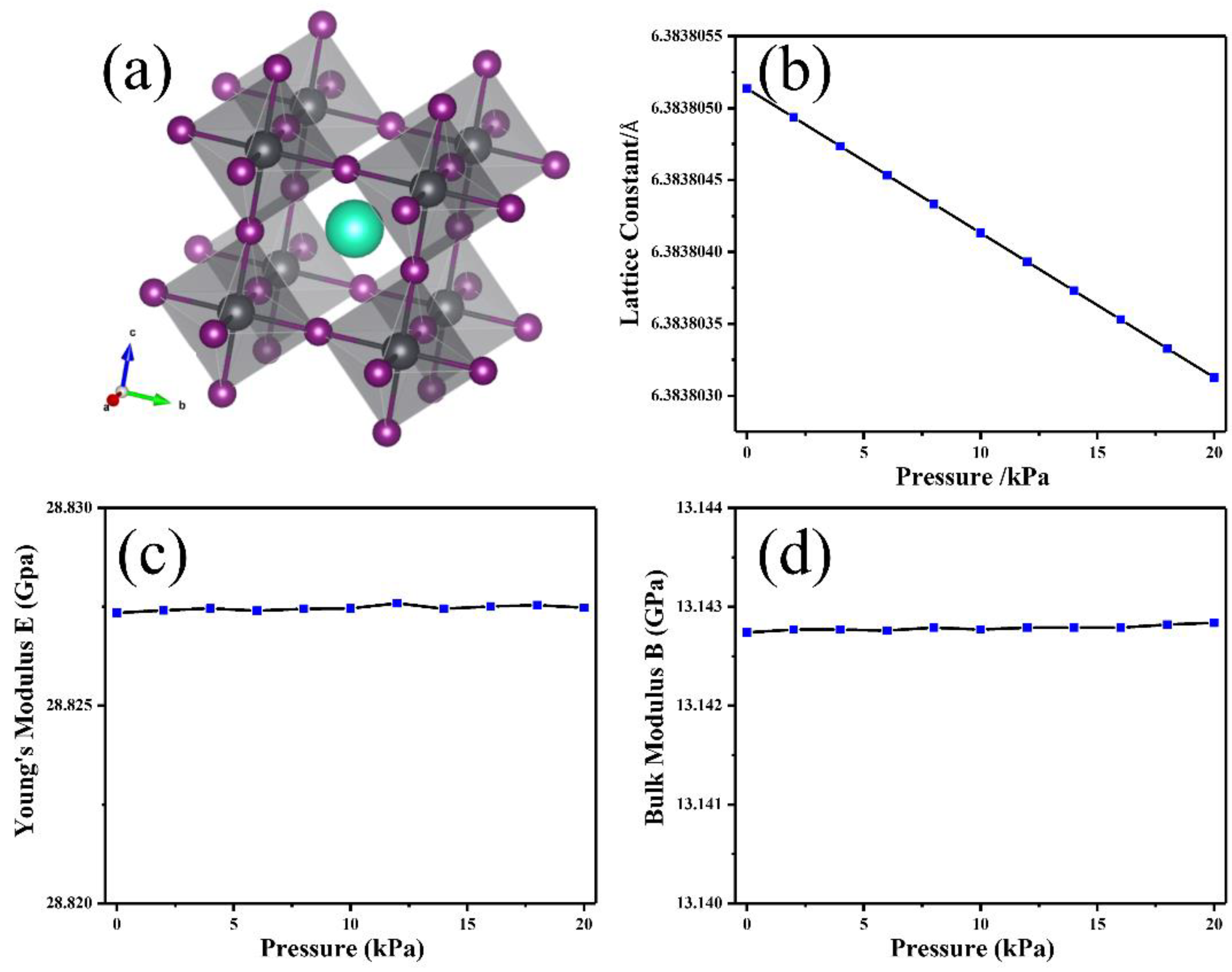
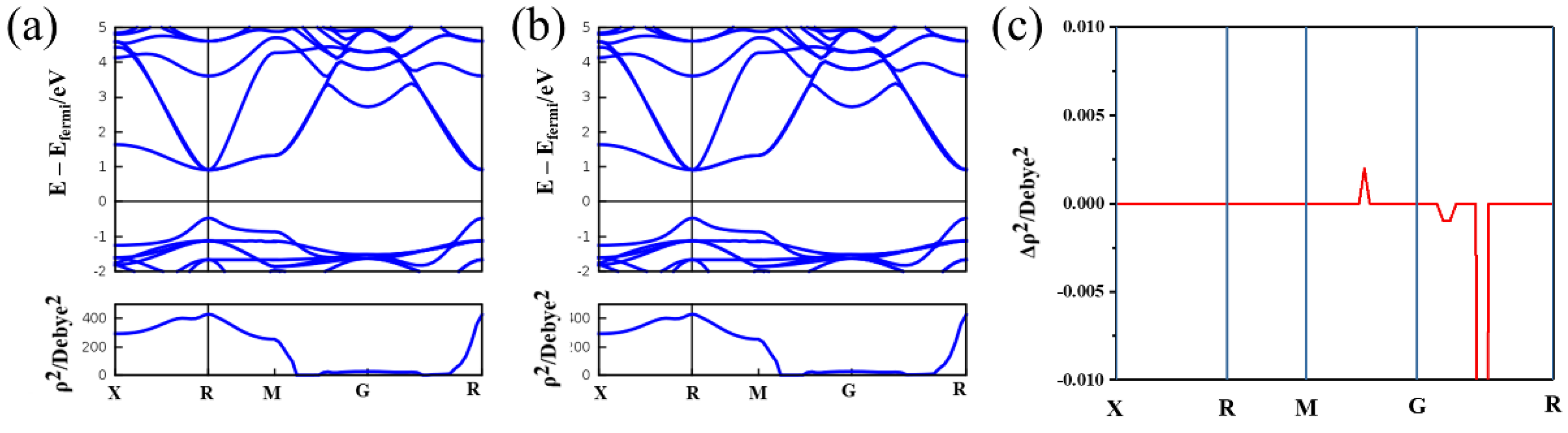
3. Results and Discussions

We firstly investigated the structural properties of CsPbI3 (Figure 1a) under pressure; the lattice constant a = b = c = 6.38 Å when no pressure is applied. The value gradually decreases as the pressure increases from 0 to 20 kPa; as shown in Figure 1b, the lattice constant decreases slowly and linearly with increasing pressure. In order to measure the resistance change of perovskite CsPbI3 due to deformation at pressure ranging from 0 to 20 kPa, the Young’s modulus E (Figure 1c) and bulk modulus B (Figure 1d) were calculated. From the theoretical calculation results, it is obvious that the Young’s modulus and bulk modulus hardly change, the Young’s modulus is 28.83 GPa and the bulk modulus is 13.14 GPa. The above results show that the lattice constants of perovskite CsPbI3 decrease slightly under the pressure range from 0 to 20 kPa, while the deformation resistance changes negligibly.
It is well known that the Young’s modulus and bulk modulus of crystal are macroscopic properties of the material, while at the microscopic level, they are determined by the strength and compressibility of chemical bonds, that is, by the composition of chemical bonds [30]. The calculation results show that the lattice constants of perovskite materials decrease slowly during the compression process, which will inevitably cause some changes in chemical bonds, while the Young’s modulus and bulk modulus are almost unchanged. To further obtain a clear insight into the phenomenon, the density of states (DOS) was calculated. Figure 2 shows the DOS of perovskite CsPbI3 under pressure 0 (Figure 2a) and 10 kPa (Figure 2b); the DOS of perovskite under pressure 10 kPa is basically the same as that under 0 kPa from the point of view of total DOS and project DOS (PDOS), the valence band maximum (VBM) is mainly composed of Pb 6s and I 5p, and the conduction band minimum (CBM) is mainly contributed by Pb 6p and I 5s. However, by subtracting the total DOS and PDOS between 0 and 10 kPa, we find that there are still some differences in the orbital contribution. As shown in Figure 2c, there is no difference in the total DOS, while the PDOS of Cs 5s increases in the energy range from −1 to −0.5 eV under 10 kPa compare to 0 kPa, the PDOS of Cs 6s decreases and the PDOS of Cs 5p increases at around −0.5 eV and decreases at around −1.0 eV. Similarly, the PDOS of Pb 5d increases at around −0.5 eV, Pb 6p decreases at around −0.5 eV, and Pb 6s increases at around 0.8 eV, I 4d and I 5s decrease at around −0.5 eV and I 5p increases at around −0.8 eV. We also calculated the total DOS, PDOS and difference comparing values under 0 kPa to that under other pressure from 0 to 20 kPa (Figures S1–S9); the PDOS of Cs is shown in Figure S10. The results show that there is no difference in total DOS, but there is a slight difference in PDOS. Therefore, we can infer that the lattice change caused by pressure is not large, so that the total DOS does not change under different pressure. Although there is a difference in the PDOS, the difference is not large enough, so the Young’s modulus and bulk modulus hardly change under pressure. The DOS will change dramatically if enough pressure is applied, and the Young’s modulus and bulk modulus will change accordingly.
The inorganic halide perovskite has made great progress in the field of photoluminescence and electroluminescence due to their excellent photoelectric properties [31,32,33]. In the assessment of the optical property of inorganic halide perovskite under pressure, the electronic band structure and transition dipole moment can play an important role [34]. Therefore, we calculated the electronic band structure and transition dipole moment of perovskite CsPbI3 under different pressure in order to study the influence of pressure on the optical properties. The calculation results are shown in Figure 3; the electronic band structure of perovskite CsPbI3 under 0 (Figure 3a) and 10 kPa (Figure 3b) is almost the same, they are all direct bandgap, the VBM and the CBM of perovskite CsPbI3 are both located at the R point, and the value of bandgap is 1.38 eV. The direct bandgap feature of CsPbI3 has been retained under a pressure range from 0 to 20 kPa (see Figures S11 and S19). The photoluminescence quantum yield (PLQY) is the ability of materials to convert absorbed light energy into photoluminescence; it is defined as the ratio of the radiative recombination rate to the sum of the radiative and non-radiative recombination rates. According to the Fermi’s golden rule, the radiative recombination rate is proportional to the transition dipole moment. Then, we calculated the transition dipole moment of perovskite CsPbI3 under different pressure to evaluate the effect of pressure on the photoluminescence property. We find that the transition dipole moment is basically the same under pressure 0 (Figure 3a) and 10 kPa (Figure 3b) from the calculation results, while the maximum transition dipole moment squared is 429 Debye2 and located at the R point, which is the same position as the VBM and CBM. Then, we obtained the difference of the transition dipole moment (Figure 3c) under pressure 0 and 10 kPa through subtracting the transition dipole moment between them, and we find that their transition dipole moment is exactly the same at the R point, and the slight difference is located in the k-point range M-G and G-R, the same is true for other pressure in the range of 0 to 20 kPa (see Figures S11 and S19). The above results indicated that the electronic band structure is almost unchanged under pressure ranging from 0 to 20 kPa, and the position of the highest PLQY remains the same, while the transition dipole moment of the other k point direction may change, so that the photoluminescence property of the perovskite CsPbI3 is almost not affected.
Lead halide perovskite has a long carrier lifetime, and the carrier cooling process is one of the reasons for the long lifetime; the hot carrier cooling occurs in the radiation recombination process after the electron excitation [35]. Ma et al. showed that the localized carriers in MAPbI3 can have random walks due to the fluctuation of electrostatic potential caused by the MA+ random rotations [36]. Zhang et al. reported the effect of polaron formation on the carrier transport properties in cubic phase CsPbI3 [37]. Mastrikov et al. also found the electron and hole polarons in PbX2 (X = F, Cl, Br) and constructed a clear picture of the corresponding electronic and atomic structures through first-principles calculations [38]. Although much progress has been made in the carriers of perovskite and lead halides, there is little literature on the influence of the pressure on the hot carrier cooling process. Next, we will study the influence with the rt-TDDFT calculation; at the first step, it will do a self-consistent field calculation with the constraint occupation numbers. So, after the first step, the charge density and the wavefunction will be updated. It is the appropriate way to describe the hot carrier cooling process. Herein, we study the hot carrier cooling process under pressure with rt-TDDFT and investigate the role of hot carrier cooling in perovskite CsPbI3. In this work, to simplify the model, we take an electron from the VBM (state-37) and put it in the CBM + 1 (state-39, see Figure 4) to represent the excited state carrier. Then, we study the electron relaxation from the CBM + 1 to the CBM, which is the hot carrier cooling process. From Figure 4a, one can see that the occupation of the state-37 (VBM, the state with a hole at first) of perovskite CsPbI3 under pressure 0 kPa increase to 2 in 10 fs, while the state-32, state-33 and state-36 occupation reduces in 10 fs, and then they start to fluctuate. Eventually, the hole is in state-32 at 100 fs, which is the hot carrier (hole) cooling process in perovskite CsPbI3 under pressure of 0 kPa. We also find that the occupation of the state-39 (CBM + 1) decreases to 0 in 30 fs, while the occupation of the state-40 (CBM + 2) and state-41 (CBM + 3) fluctuates up to 50 fs, and then they stay roughly constant. The fluctuation range is within 0.5, and further analysis shows that the occupation of state-38 (CBM) increases continuously after 50 fs and increases to 0.3 at 90 fs, which is the hot electron cooling process. The change in occupation will bring about a change in the orbital energy; we find that the orbital energy of state-37 (VBM) continues to decrease from Figure 4d, which shows that the state-37 (VBM) tends to be stable with the hot hole cooling. As for the orbital energy of state-38 (CBM), it has been basically stable, which is due to the perovskite CsPbI3 having a long carrier lifetime and the electrons having not relaxed into the orbital. The conclusion is further supported by the results of the evolution of perovskite CsPbI3 excited carriers (Figure S20a); the electrons above the CBM kept going back and forth in 50 fs, without relaxing into the CBM, while the holes in the VBM gradually relaxed into lower energy orbitals, and the VBM was rapidly filled with electrons. After applying pressure to the perovskite CsPbI3, the hot carrier cooling process on different orbitals is obviously different from that without pressure. As shown in Figure 4b,c, the number of electrons in the state-37 (VBM) increases to 2 electrons at 10 fs; however, the lost maximum number of electrons in state-32 occurs at 30 fs and 20 fs under pressure 10 kPa and 20 kPa, respectively, which are different from that without pressure. In addition, we observed that the state-39 (CBM + 1) loses an electron to state-40 (CBM + 2) at 10 fs in Figure 4b,c, and then, the electrons oscillate in the orbital above the state-38 (CBM). The change trend of orbital energy is similar to that when no pressure is applied, the orbital energy of the state-37 (VBM) decreases, and the state-38 (CBM) is basically unchanged for not having any electrons that relaxed (see Figure 4e,f), which is consistent with the trend of the evolution of perovskite CsPbI3 excited carriers under pressure 10 kPa (Figure S20b) and 20 kPa (Figure S20c). Thus, we can know that the electrons and holes generated after the photoexcitation of perovskite CsPbI3 do not immediately relax to the VBM and CBM, but they fluctuate back and forth in the orbital near them, which may be the reason for the long carrier lifetime of perovskite.
In order to further analyze the above hot carrier cooling process, we calculated the evolution charge density distribution of VBM and CBM in perovskite CsPbI3 under different pressure (see Figure 5). From the calculation results, we can know that the charge density of VBM increases more than the CBM under all pressure, which is consistent with the calculation of the hot carrier cooling process; the number of electrons in CBM hardly changes, but the number of electrons in VBM increases significantly with time. The contribution of the iodine orbital to the VBM increases under pressure 10 kPa and 20 kPa compared to 0 kPa (see Figure 5b,f,j). At the same time, the change of electrical conductivity will be mainly affected by the electron orbital under the premise that the Young’s modulus is basically unchanged [21,22]; therefore, the difference of charge density under different pressure will lead to the difference of intrinsic electrical conductivity of perovskite CsPbI3, which will make the material have different resistance under the same macroscopic condition. Furthermore, we calculated the theoretical room-temperature carrier-concentration-dependent electrical conductivities of perovskite CsPbI3 under pressure 0, 10 and 20 kPa to obtain the effect of pressure on electrical conductivity. As shown in Figure 6, the larger the pressure, the larger the electrical conductivity of perovskite CsPbI3 over all carrier concentrations, in other words, the less the resistance of the macroscopic size. The property in which the resistance of perovskite CsPbI3 decreases as the pressure increases has great potential for preparing the piezoresistive materials and obtaining highly precision pressure sensors.

4. Conclusions

In summary, we have investigated the effect of pressure on the structure, electronic properties and hot carrier cooling process of perovskite CsPbI3. We observed that the lattice constant decreases linearly with pressure increases, and the Young’s modulus and bulk modulus remain almost constant. Then, we studied the changes in DOS and electronic band structure under pressure, and we found that the changes were very small in range from 0 to 20 kPa, but there are still minor differences, which result in changes in the hot carrier cooling process and electrical conductivity: the time of the hot hole cooling to the VBM under pressure becomes shorter than that under no pressure, while the time of hot electron cooling to the CBM shows no significant difference, the electron fluctuates between different energy levels above the CBM, and the continuous vibration of carrier in the non-VBM and non-CBM region is beneficial to the prolongation of carrier lifetime. The phenomenon by which the electrical conductivity increases with increasing pressure will cause the resistance of the same macroscopic size changes, indicating that perovskite CsPbI3 has great potential for preparing high-precision piezoresistive pressure sensors. We believe this work may provide theoretical insights for researchers in the field and bring more opportunities for the field of pressure detection.

Supplementary Materials

The following supporting information can be downloaded at: https://www.mdpi.com/article/10.3390/cryst12050648/s1. Figures S1–S9: The DOS of perovskite CsPbI3 under different pressure (0~20 kPa); Figure S10: The PDOS of Cs in perovskite CsPbI3 under different pressure (0~20 kPa); Figures S11–S19: The electronic band structure and transition dipole moment under different pressure (2~18 kPa); Figure S20: The evolution of perovskite CsPbI3 excited carriers under pressure 0, 10 and 20 kPa.

Author Contributions

Conceptualization, S.H. and M.J.; methodology, S.H.; software, S.H.; validation, S.H., M.J. and X.H.; formal analysis, X.W.; investigation, M.J.; resources, X.H.; data curation, S.H.; writing—original draft preparation, S.H.; writing—review and editing, M.J.; visualization, X.W.; supervision, S.H.; project administration, X.W.; funding acquisition, X.H. All authors have read and agreed to the published version of the manuscript.

Funding

This research was funded by the National Natural Science Foundation of China (52174222), the China Postdoctoral Science Foundation funded project (2021M693408), Jiangsu Planned Projects for Postdoctoral Research Funds (2021K600C), Natural Science Fund project in Jiangsu Province (BK20210494) and Heilongjiang Provincial Natural Resources Foundation Joint Guide Project (Grant No. LH2020E098).

Institutional Review Board Statement

Not applicable.

Informed Consent Statement

Not applicable.

Data Availability Statement

Not applicable.

Conflicts of Interest

The authors declare no conflict of interest.

References

  1. Shi, D.; Adinolfi, V.; Comin, R.; Yuan, M.; Alarousu, E.; Buin, A.; Chen, Y.; Hoogland, S.; Rothenberger, A.; Katsiev, K.; et al. Low trap-state density and long carrier diffusion in organolead trihalide perovskite single crystals. Science 2015, 347, 519–522. [Google Scholar] [CrossRef] [PubMed] [Green Version]
  2. Song, J.; Zhao, L.; Huang, S.; Yan, X.; Qiu, Q.; Zhao, Y.; Zhu, L.; Qiang, Y.; Li, H.; Li, G. A p-p+ homojunction-enhanced hole transfer in inverted planar perovskite solar cells. ChemSusChem 2021, 14, 1396–1403. [Google Scholar] [CrossRef] [PubMed]
  3. Zhang, F.; Zhong, H.; Chen, C.; Wu, X.G.; Hu, X.; Huang, H.; Han, J.; Zou, B.; Dong, Y. Brightly luminescent and color-tunable colloidal CH3NH3PbX3 (X = Br, I, Cl) quantum dots: Potential alternatives for display technology. ACS Nano 2015, 9, 4533–4542. [Google Scholar] [CrossRef]
  4. Zhou, Q.; Bai, Z.; Lu, W.G.; Wang, Y.; Zou, B.; Zhong, H. In situ fabrication of halide terovskite nanocrystal-embedded polymer composite films with enhanced photoluminescence for display backlights. Adv. Mater. 2016, 28, 9163–9168. [Google Scholar] [CrossRef] [PubMed]
  5. Wang, L.; Zhou, H.; Hu, J.; Huang, B.; Sun, M.; Dong, B.; Zheng, G.; Huang, Y.; Chen, Y.; Li, L.; et al. A Eu3+-Eu2+ ion redox shuttle imparts operational durability to Pb-I perovskite solar cells. Science 2019, 363, 265–270. [Google Scholar] [CrossRef] [PubMed]
  6. Huang, S.; Tang, G.; Huang, H.; Wu, X.; Zhou, P.M.; Zou, L.; Xie, L.; Deng, J.M.; Wang, X.; Zhong, H.Z.; et al. Enhanced piezo-response in copper halide perovskites based PVDF composite films. Sci. Bull. 2018, 63, 1254–1259. [Google Scholar] [CrossRef] [Green Version]
  7. Gao, L.L.; Li, X.; Traoré, B.; Zhang, Y.; Fang, J.; Han, Y.; Even, J.; Katan, C.; Zhao, K.; Liu, S.; et al. m-Phenylenediammonium as a new spacer for Dion-Jacobson two-dimensional perovskites. J. Am. Chem. Soc. 2021, 143, 12063–12073. [Google Scholar] [CrossRef]
  8. Hou, Y.; Du, X.; Scheiner, S.; McMeekin, D.P.; Wang, Z.; Li, N.; Killian, M.S.; Chen, H.; Richter, M.; Levchuk, I.; et al. A generic interface to reduce the efficiency-stability-cost gap of perovskite solar cells. Science 2017, 358, 1192–1197. [Google Scholar] [CrossRef] [Green Version]
  9. Kojima, A.; Teshima, K.; Shirai, Y.; Miyasaka, T. Organometal halide perovskites as visible-light sensitizers for photovoltaic cells. J. Am. Chem. Soc. 2009, 131, 6050–6051. [Google Scholar] [CrossRef]
  10. Han, D.; Imran, M.; Zhang, M.; Chang, S.; Wu, X.; Zhang, X.; Tang, J.; Wang, M.; Ali, S.; Li, X.; et al. Efficient light-emitting diodes based on in situ fabricated FAPbBr3 nanocrystals: The enhancing role of the ligand-assisted reprecipitation process. ACS Nano 2018, 12, 8808–8816. [Google Scholar] [CrossRef]
  11. Fang, Y.; Dong, Q.; Shao, Y.; Yuan, Y.; Huang, J.S. Highly narrowband perovskite single-crystal photodetectors enabled by surface-charge recombination. Nat. Photonics 2015, 9, 679–686. [Google Scholar] [CrossRef]
  12. Wang, L.; Meng, L.; Chen, L.; Huang, S.; Wu, X.; Dai, G.; Deng, L.; Han, J.; Zou, B.; Zhang, C.; et al. Ultralow-threshold and color-tunable continuous-wave lasing at room-temperature from in situ fabricated perovskite quantum dots. J. Phys. Chem. Lett. 2019, 10, 3248–3253. [Google Scholar] [CrossRef] [PubMed]
  13. Fu, Q.; Draxl, C. Hybrid organic-inorganic perovskites as promising substrates for Pt single-atom catalysts. Phys. Rev. Lett. 2018, 122, 46101. [Google Scholar] [CrossRef] [PubMed] [Green Version]
  14. Wang, K.; Li, G.; Wang, S.; Liu, S.; Sun, W.; Huang, C.; Wang, Y.; Song, Q.; Xiao, S. Dark-field sensors based on organometallic halide perovskite microlasers. Adv. Mater. 2018, 30, 1801481. [Google Scholar] [CrossRef]
  15. Ma, Z.; Liu, Z.; Lu, S.; Wang, L.; Feng, X.; Yang, D.; Wang, K.; Xiao, G.; Zhang, L.; Redfern, S.A.T.; et al. Pressure-induced emission of cesium lead halide perovskite nanocrystals. Nat. Commun. 2018, 9, 4506. [Google Scholar] [CrossRef]
  16. Xia, M.; Yuan, J.H.; Luo, J.; Pan, W.; Wu, H.; Chen, Q.; Xue, K.H.; Miao, X.; Niu, G.; Tang, J. Two-dimensional perovskites as sensitive strain sensors. J. Mater. Chem. C 2020, 8, 3814–3820. [Google Scholar] [CrossRef]
  17. Dai, G.; Wang, L.; Cheng, S.; Chen, Y.; Liu, X.; Deng, L.; Zhong, H. Perovskite quantum dots based optical Fabry-Pérot pressure sensor. ACS Photonics 2020, 7, 2390–2394. [Google Scholar] [CrossRef]
  18. Almassri, A.M.; Wan Hasan, W.Z.; Ahmad, S.A.; Ishak, A.J.; Ghazali, A.M.; Talib, D.N.; Wada, C. Pressure sensor: State of the art, design, and application for robotic hand. J. Sens. 2015, 12, 846487. [Google Scholar] [CrossRef] [Green Version]
  19. Ahmad, W.; Khan, J.; Niu, G.; Tang, J. Inorganic CsPbI3 perovskite-based solar cells: A choice for a tandem device. Solar RRL 2017, 1, 1700048. [Google Scholar] [CrossRef]
  20. Huang, S.; Shan, H.; Xuan, W.; Xu, W.; Hu, D.; Zhu, L.; Huang, C.; Sui, W.; Xiao, C.; Zhao, Y.; et al. High-performance humidity sensor based on CsPdBr3 nanocrystals for noncontact sensing of hydromechanical characteristics of unsaturated soil. Phys. Status Solidi RRL 2022, 2200017. [Google Scholar] [CrossRef]
  21. Ke, F.; Wang, C.; Jia, C.; Wolf, N.R.; Yan, J.; Niu, S.; Devereaus, T.P.; Karunadasa, H.I.; Mao, W.L.; Lin, Y. Preserving a robust CsPbI3 perovskite phase via pressure-directed octahedral tilt. Nat. Commun. 2021, 12, 461. [Google Scholar] [CrossRef] [PubMed]
  22. Liang, Y.; Huang, X.; Huang, Y.; Wang, X.; Li, F.; Wang, Y.; Tian, F.; Liu, B.; Shen, Z.X.; Cui, T. New metallic ordered phase of perovskite CsPbI3 under pressure. Adv. Sci. 2019, 6, 1900399. [Google Scholar] [CrossRef] [PubMed] [Green Version]
  23. Satpathy, S.; Christensen, N.E.; Jepsen, O. Metallization of CsI under pressure: Theoretical results. Phys. Rev. B 1985, 32, 6793. [Google Scholar] [CrossRef] [PubMed]
  24. Jayaraman, A.; Maines, R.G.; Chattopadhyay, T. Pressure-induced structural transitions in PbI2: A high-pressure Raman and optical absorption study. Pramana 1986, 27, 449–457. [Google Scholar] [CrossRef]
  25. Jia, W.; Cao, Z.; Wang, L.; Fu, J.; Chi, X.; Gao, W.; Wang, L.W. The analysis of a plane wave pseudopotential density functional theory code on a GPU machine. Comput. Phys. Commun. 2013, 184, 9–18. [Google Scholar] [CrossRef]
  26. Perdew, J.P.; Burke, K.; Ernzerhof, M. Generalized gradient approximation made simple. Phys. Rev. Lett. 1996, 78, 1396. [Google Scholar] [CrossRef] [Green Version]
  27. Yang, J.; Xi, L.; Zhang, W.; Chen, L.D.; Yang, J. Electrical transport properties of filled CoSb3 skutterudites: A theoretical study. J. Electron. Mater. 2009, 38, 1397–1401. [Google Scholar] [CrossRef]
  28. Xi, L.; Pan, S.; Li, X.; Xu, Y.; Ni, J.; Sun, X.; Yang, J.; Luo, J.; Xi, J.; Zhu, W.; et al. Discovery of high-performance thermoelectric chalcogenides through reliable high-throughput material screening. J. Am. Chem. Soc. 2018, 140, 10785–10793. [Google Scholar] [CrossRef]
  29. Jia, W.; Fu, J.; Cao, Z.; Wang, L.; Chi, X.; Gao, W.; Wang, L.W. Fast plane wave density functional theory molecular dynamics calculations on multi-GPU machines. J. Comput. Phys. 2013, 251, 102–115. [Google Scholar] [CrossRef]
  30. Wei, L.; Chen, J.F.; Qinyu, H.; Teng, W. Electronic and elastic properties of MoS2. Phys. B Condens. Matter 2010, 405, 2498–2502. [Google Scholar] [CrossRef]
  31. Cherniukh, I.; Rainò, G.; Stöferle, T.; Burian, M.; Travesset, A.; Naumenko, D.; Amenitsch, H.; Erni, R.; Mahrt, R.F.; Bodnarchuk, M.I. Perovskite-type superlattices from lead halide perovskite nanocubes. Nature 2021, 593, 535–542. [Google Scholar] [CrossRef] [PubMed]
  32. Gandini, M.; Villa, I.; Beretta, M.; Gotti, C.; Imran, M.; Carulli, F.; Fantuzzi, E.; Sassi, M.; Zaffalon, M.; Brofferio, C.; et al. Efficient, fast and reabsorption-free perovskite nanocrystal-based sensitized plastic scintillators. Nat. Nanotechnol. 2020, 15, 462–468. [Google Scholar] [CrossRef] [PubMed]
  33. Lin, K.B.; Xing, J.; Quan, L.N.; de Arquer, F.P.G.; Gong, X.; Lu, J.; Xie, L.; Zhao, W.; Zhang, D.; Yan, C.; et al. Perovskite light-emitting diodes with external quantum efficiency exceeding 20 percent. Nature 2018, 562, 245–248. [Google Scholar] [CrossRef] [PubMed]
  34. Luo, J.; Wang, X.; Li, S.; Liu, J.; Guo, Y.; Niu, G.; Yao, L.; Fu, Y.; Gao, L.; Dong, Q.; et al. Efficient and stable emission of warm-white light from lead-free halide double perovskites. Nature 2018, 563, 541–545. [Google Scholar] [CrossRef]
  35. Li, J.; Jing, Q.; Xiao, S.; Gao, Y.; Wang, Y.; Zhang, W.; Sun, X.W.; Wang, K.; He, T. Spectral dynamics and multiphoton Aabsorption properties of all-inorganic perovskite nanorods. J. Phys. Chem. Lett. 2020, 11, 4817–4825. [Google Scholar] [CrossRef]
  36. Ma, J.; Wang, L.W. The nature of electron mobility in hybrid perovskite CH3NH3PbI3. Nano Lett. 2017, 17, 3646–3654. [Google Scholar] [CrossRef]
  37. Zhang, H.; Debroye, E.; Steele, J.A.; Roeffaers, M.B.J.; Hofkens, J.; Wang, H.I.; Bonn, M. Highly mobile large polarons in black phase CsPbI3. ACS. Energy Lett. 2021, 6, 568–573. [Google Scholar] [CrossRef]
  38. Mastrikov, Y.; Chuklina, N.G.; Sokolov, M.; Popov, A.; Gryaznov, D.; Kotomin, E.A. Small radius electron and hole polarons in PbX2 (X = F, Cl, Br) crystals: A computational study. J. Mater. Chem. C 2021, 9, 16536–16544. [Google Scholar] [CrossRef]
Figure 1. The crystal structure and mechanical properties of perovskite CsPbI3. (a) The crystalline structure of cubic CsPbI3. (b) Lattice constants, (c) Young’s modulus E and (d) Bulk modulus B under different pressure.
Crystals 12 00648 g001
Figure 2. The DOS of perovskite CsPbI3 under different pressure. (a) 0 kPa. (b) 10 kPa. (c) The DOS difference between 0 and 10 kPa.
Crystals 12 00648 g002
Figure 3. The electronic band structure and transition dipole moment. The upper of (a,b) is the electronic band structure under 0 and 10 kPa, respectively, and the bottom of (a,b) is the transition dipole moment. (c) The transition dipole moment difference between 0 and 10 kPa.
Crystals 12 00648 g003
Figure 4. The hot carrier cooling process in perovskite CsPbI3 under different pressure. (a), (b) and (c) represent the change in occupation state under pressure 0 kPa, 10 kPa and 20 kPa, respectively. (d), (e) and (f) represent the change in orbital energy under pressure 0 kPa, 10 kPa and 20 kPa, respectively.
Crystals 12 00648 g004
Figure 5. The evolution charge density distribution corresponding to the VBM and CBM of perovskite CsPbI3 under pressure. (a), (e) and (i) represent the CBM under 0, 10 and 20 kPa at 0 fs, respectively. (b), (f) and (j) represent the VBM under 0, 10 and 20 kPa at 0 fs, respectively. (c), (g) and (k) represent the CBM under 0, 10 and 20 kPa at 50 fs, respectively. (d), (h) and (l) represent the VBM under 0, 10 and 20 kPa at 50 fs, respectively. The charge contours are set to a critical charge density of 0.0014 e Å-3 for CBM and 0.0043 e Å-3 for VBM.
Crystals 12 00648 g005
Figure 6. (a) The carrier-concentration-dependent electrical conductivities for perovskite CsPbI3 under pressure 0, 10 and 20 kPa. (b) is a partial enlargement of (a).
Crystals 12 00648 g006
Publisher’s Note: MDPI stays neutral with regard to jurisdictional claims in published maps and institutional affiliations.

