Article

Effect of Flux Rate Variation at Fixed V/III Ratio on Semi-Polar (112¯2) GaN: Crystal Quality and Surface Morphology Study

1
Low Dimensional Materials Research Centre, Department of Physics, Faculty of Science, Universiti Malaya, Kuala Lumpur 50603, Selangor, Malaysia
2
Nanotechnology Research Centre, Department of Physics, Faculty of Science and Mathematics, Universiti Pendidikan Sultan Idris, Tanjong Malim 35900, Perak, Malaysia
*
Authors to whom correspondence should be addressed.
Crystals 2022, 12(2), 247; https://doi.org/10.3390/cryst12020247
Submission received: 22 December 2021 / Revised: 7 February 2022 / Accepted: 9 February 2022 / Published: 11 February 2022
(This article belongs to the Special Issue GaN-Based Materials and Devices)

Abstract

:
We report on the crystal improvement of semi-polar (11 2 ¯ 2) gallium nitride epitaxy layer on m-plane (10 1 ¯ 0) sapphire substrate by changing the flux rate at a fixed V/III ratio. The high-resolution X-ray diffraction (HR-XRD) analysis showed that lower flux rate enhanced the crystal quality of GaN epitaxy with the lowest FWHM values of 394 and 1173 arc seconds at [ 11 ¯ 23] and [1 1 ¯ 00] planes, respectively. In addition, Raman spectroscopy showed that flux rate did not affect the stress state of the GaN crystal. However, atomic force microscopy (AFM) micrograph depicted an anomalous trend where the lowest flux rate produces roughest surface with RMS roughness of 40.41 nm. Further analysis of AFM results on the undulation period length along [ 11 ¯ 23] and [1 1 ¯ 00] directions is carried out. It shows that as the growth rate decreases, the average undulation period along [ 11 ¯ 23] and [1 1 ¯ 00] directions increases from 2.59 µm and 1.90 µm to 3.52 µm and 3.52 µm, respectively. The mechanism for the surface roughening at the lower flux rate is then explained by using the adatom surface diffusion relation L   ~   D τ .

Graphical Abstract

1. Introduction

III-nitride based optoelectronic devices have been of great interest as an alternative to conventional light bulbs due to their wide band gap, ranging from 0.67 to 3.4 eV, which includes the full visible light spectrum and their high emission efficiency [1,2,3]. The most commonly used material for LED is gallium nitride (GaN) which typically grows along the c-direction [4,5]. However, LED grown on the c-plane suffers a large quantum-confined stark effect (QCSE) due to the existence of piezoelectric and spontaneous polarization in the quantum well region [6]. This phenomenon caused the separation of the electron-hole wave functions and increased the recombination time, thus lessening the efficiency of the device [6,7,8]. The impact became significant in longer wavelength LED as the higher indium incorporation induced more lattice mismatch in the quantum well [9]. In order to overcome this problem, GaN based LED is grown on a non- and semi-polar crystal orientation [10]. Devices grown along these orientations have been proved to have higher internal and external quantum efficiency [11]. However, for longer wavelength devices, semi-polar orientation is preferred as non-polar orientation has less indium incorporation efficiency [12,13]. On the flip side, semi-polar (11 2 ¯ 2) GaN, for example, suffers from high defect density; 98% is contributed by partial dislocations (PDs) and basal stacking faults (BSFs), and 2% is caused by a-type perfect dislocations [14,15]. Numerous efforts, such as epitaxial lateral overgrowth (ELOG) [16], AlN/GaN multilayer, silicon nitride (SiNx) interlayer [17], double AlN or GaN nucleation layers [18], patterned sapphire substrates [19] and graded superlattices [20] have been explored to solve this problem to achieve an enhanced crystal quality and surface morphology. Growth parameters, such as temperature [21], V/III ratio [22] and reactor pressure [23,24], have been widely discussed to understand the influence of the growth process. To achieve a good GaN layer researchers will normally combine the growth parameters utilizing a two-step process to achieve 3D layers first using a rather lower V/III ratio and temperature and then a higher V/III ratio and temperature for surface smoothing [25]. However, to the authors’ best knowledge, there is no research yet reported on the growth parameter of the flux rate at a fixed V/III ratio on semi-polar GaN growth.
In this report, we demonstrate the improvement of crystal quality in semi-polar (11 2 ¯ 2) GaN by varying the flux rate at a fixed V/III ratio. The effect on crystal quality and surface morphology is evaluated by using high resolution X-ray diffraction (HR-XRD) and atomic force microscopy (AFM) while room temperature Raman spectroscopy is used to investigate the stress within the GaN film.

2. Experimental Methods

Semi-polar (11 2 ¯ 2) GaN epi-layers were grown on an m-plane (10 1 ¯ 0) sapphire substrate via metal-organic chemical vapor deposition (MOCVD) (SR-2000, Taiyo Nippon Sanso, Japan). The precursors used were trimethylaluminum (TMA) for aluminum, trimethylgallium (TMG) for gallium and ammonia (NH3) for nitrogen. The m-plane sapphire underwent a hydrogen cleaning for 10 min at a temperature of 1125 °C. After nitridation, an AlN nucleation layer of 100 nm was grown at the temperature of 1050 °C before the growth of the GaN layer. Next, GaN was grown at a fixed V/III ratio of 118 at a temperature of 1050 °C. The growth time was varied to ensure that an epitaxial layer thickness of around 4.65 µm was achieved. Reactor pressure was set to 13.3 kPa during the growth. The TMG and NH3 flux rate for GaN epi-layer growth were varied sequentially during the epitaxy growth. The experiment series is tabulated in Table 1 with their respective flux rate and growth rate, while Figure 1 illustrates the epitaxy structure grown in this experiment. Hydrogen (H2) was used as a gas carrier throughout the growth.
The structural properties of the GaN epitaxy layer were characterized by Rigaku SmartLab high-resolution X-ray diffraction (HR-XRD) with 2-bounce (220) Ge monochromator (with incident and receiving slits set at 1 mm) without an analyzer crystal at the receiving optics and RT Raman Spectroscopy (inVia, Renishaw), while surface morphology was examined by Park System NX-10 atomic force microscopy (AFM) via non-contact mode.

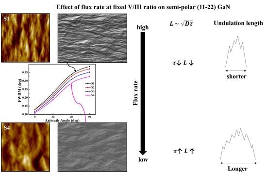
3. Result and Discussion

To investigate the effect of flux rate on the crystal quality of the grown GaN epilayer, XRD measurement was carried out. Only (11 2 ¯ 2) diffraction peaks were observed for all samples, as shown in Figure 2 in the HR-XRD 2θ-ω scans. Hence, we can conclude that varying the flux rate while keeping a fixed V/III ratio at this scale did not affect the crystallographic formation of semi-polar (11 2 ¯ 2) GaN epitaxy. To further evaluate the crystal quality of the as-grown samples, on-axis ω-scans were carried out.
Figure 3a shows the crystal quality of semi-polar (11 2 ¯ 2) GaN evaluation performed via on-axis X-ray rocking curve (XRC) as a function of the azimuthal angle (φ). The analysis was done over a 90° range with an interval of 30°, where 0° and 90° correspond to directions [ 11 ¯ 23] and [1 1 ¯ 00], respectively. It is noted that the XRC FWHM for all samples along [1 1 ¯ 00] is broader than [ 11 ¯ 23], which are similar to the reported observations on (11 2 ¯ 2) GaN [18,26,27,28]. For example, [ 11 ¯ 23] and [1 1 ¯ 00] planes of sample S1 shown to have the FWHM of 464 and 1390 arcsec, respectively. This trend is due to the strain from the different growth rates in the a- and c-direction and lattice mismatch between (11 2 ¯ 2) GaN and sapphire [29]. Different plane broadening is also reported due to the larger mosaic tilt and/or reduced in coherent length (smaller size of the mosaic blocks) [27]. By decreasing the flux rate, it helped to improve the crystal quality, which is reflected by the FWHMs narrowing for each azimuthal angle. As the flux rate is reduced to S4, a crystalline quality at [ 11 ¯ 23] and [1 1 ¯ 00] planes achieved 394 and 1173 arcsec, respectively. The improvement in crystal quality might be attributed to the increase in the surface V/III ratio, as more ammonia can decompose at slower growth rate. It has been reported that a higher V/III ratio GaN is utilized to reduce defects where most of the dislocation bending process took place [30,31,32]. A similar defect reduction mechanism in semi-polar (11 2 ¯ 2) GaN has also been further discussed in ref. [23,33,34].
Figure 3b shows the tilt measured between two omega (ω) rocking curves peaks of the symmetric (11 2 ¯ 2) GaN diffraction along [ 11 ¯ 23] and [1 1 ¯ 00] directions versus the growth rate. The tilt is due to the reduction of defects (especially BSFs) at AlN/GaN heterointerface and can be indirectly related to BSFs [35]. Usually, a larger tilt is connected to an improved surface. However, the tilt of all samples shown is small (≤0.11°), indicating that less BSFs are annihilated by varying the flux rate at a fixed V/III ratio.
Figure 4a,b show the RSMs around symmetric (11 2 ¯ 2) GaN on m-plane sapphire reflection for sample S1 and S4 along directions [1 1 ¯ 00] and [ 11 ¯ 23], respectively. Almost no tilt was observed in Figure 4a for both S1 and S4, indicating that the film was grown coherently along the direction. However, the RSMs in Figure 4b show a significant offset in Qx for the substrate and the epitaxial layer peaks, indicating an epitaxial tilt, α. Detailed discussion about the epitaxial tilt in (11 2 ¯ 2) nitrides has been reported in ref. [36,37]. Also, reports have shown that macroscopic tilts are related to the misfit dislocation formed at the heterointerface, resulting in the relaxation of the epitaxial layer [38,39]. The tilt angles for S1, S2, S3 and S4 are 0.22°, 0.27°, 0.30°and 0.34°, respectively. As the flux rate decreases, an increase in tilt is observed. In addition, a diffuse scattering (DS) streak parallel to [0001] direction can be seen in all samples. It has been reported that the DS steak is correlated with the presence of BSFs and PDs [18,36]. A shorter DS streak was observed in S4 compared to S1, indicating a reduction in BSFs and PDs as the flux rate decreases, which agrees with the on-axis result.
Room temperature Raman spectroscopy using z(xx) z ¯ scattering configuration was used to examine the effect of the flux rate on the compressive stress of all samples. As shown in Figure 5a, the peaks for (10 1 ¯ 0) sapphire substrate are found at 378, 416, 741 cm−1 whereas the peaks of A1, E1 and E2 are responsible for semi-polar GaN epitaxial layer [40]. It is known that the E2 mode is sensitive to the in-plane stress of the GaN layer; hence, any shifting to a lower or higher value of 568 cm−1 (standard stress-free GaN E2 peak value) indicates a tensile or compressive strain. However, none of the samples deviate from the critical point; elucidating the flux rate did not have a significant effect on the GaN in-plane stress. The FWHM of the E2 peak can also be utilized to exhibit the crystal quality of the GaN layer [41]. Figure 5b shows that the FWHM of GaN E2 peaks decreased from S1 to S4, suggesting that the increase in the E2 peaks as flux rate decreases are in agreement with the HR-XRD on-axis XRC measurements. We then carried out AFM measurement to probe the effect of the flux rate on the surface morphology.
Figure 6a shows the line profiles extracted from the AFM micrograph along [ 11 ¯ 23] (red) and [1 1 ¯ 00] (green) directions and (b) examples of their corresponding line profiles are extracted. The statistical evaluation of the undulation period length of both directions is shown in Figure 6c,d, along with the undulation amplitude which is the maximum height difference for the undulations. Figure 6c only shows the long undulation period length measured in [1 1 ¯ 00] (green) direction, as indicated by a dashed line in Figure 6b. The arrowhead feature observed in Figure 6a is a result of anistropic surface diffusion due to interference between undulations across [ 11 ¯ 23] and [1 1 ¯ 00] [42]. Undulation is formed by adatom diffusion and its period is proportional to the diffusion length. For the (11 2 ¯ 2) surface, undulation with high spatial frequency is oriented along [1 1 ¯ 00] which exhibits a high diffusion barrier on the (11 2 ¯ l)-type surface. For (11 2 ¯ 2) surfaces, the [10 1 ¯ 1] plane are tilted by 26° towards [1 1 ¯ 00], therefore undulations along [1 1 ¯ 00] are stabilized by the presence of (10 1 ¯ 1) micro-facets [43]. Based on the result in Figure 6c, the undulation period length along both directions follows an increasing trend which suggests that these undulations are connected to the decreasing growth rate. As the growth rate decreases from S1 to S4, the average undulation period along the [ 11 ¯ 23] and [1 1 ¯ 00] directions increase from 2.59 µm and 1.90 µm to 3.52 µm and 3.52 µm, respectively. A longer undulation period in the [ 11 ¯ 23] direction than in the [1 1 ¯ 00] direction is expected, as their activation energies are 0.8 and 1.3 eV, respectively, where a similar observation is reported in [42]. Similar observations are also found on the increasing undulation amplitude as growth rate decreases. The increase in undulation period and amplitude when decreasing the growth rate represents an increase in the arrowhead size. This might be explained by using the adatom surface diffusion relation:
L   ~   D τ
where L is the diffusion length, τ is the adatom lifetime on the surface and D is the diffusion constant. The D is related to temperature but the temperature throughout the growth is constant, implying the D is unaffected and, hence, the affecting factor left is τ . At a lower flux rate, the growth rate is also low and there are less incoming adatoms to the surface, causing adatoms on the surface to have a longer τ ; hence, the diffusion length is higher, which leads to longer undulation period and bigger arrowhead. In contrast, at a higher flux rate, a higher growth rate will cause more incoming adatoms which disrupt the surface diffusion and decrease the τ ; hence, resulting in a shorter undulation period and smaller arrowhead. Moreover, a slower growth rate also means that the NH3 has more time to decompose. Hence reducing the growth rate will increase the actual surface V/III ratio despite keeping the input ratio constant. This is the same reason that surfaces become more N-rich at higher pressures (and some total flow) since the NH3 has more time to decompose, which causes the surface roughening [34].
Then, the ratio of the undulation period across [ 11 ¯ 23] to [1 1 ¯ 00] for all samples with their respective RMS roughness values are tabulated in Table 2. As observed from Table 2, the ratio of the undulation period reduces as the flux rate decreases. The ratio decreases from 1.36 of sample S1 to 1.00 of sample S4 which implies that the increase of the undulation period in [1 1 ¯ 00] is greater than in the [ 11 ¯ 23] directions. This may be due to the increasing surface roughness or elongated undulations along the [1 1 ¯ 00] direction which hinders the diffusion length of adatoms along the [ 11 ¯ 23] direction.
To verify the validity of the trend obtained in the results above, the experiment was then repeated at a higher V/III ratio of 600 where the TMG and NH3 flux were varried sequentially. All the samples grown in this series are named Rn (where n = 1, 2 and 3). The summary of growth parameters adapted and all of the characterization values were tabulated in the Table 3 below.
All the samples grown were verified to be single crystalline semi-polar (11 2 ¯ 2) GaN using HR-XRD 2θ-ω scans (not shown here). Based on Table 3, the on-axis XRC FWHM values for both the [ 11 ¯ 23] and [1 1 ¯ 00] directions decreased as the flux rate decreased, showing a parallel trend with the results above where dislocations and BPSFs are reduced and crystal quality is enhanced from R1 to R3 with the FWHM values at φ = 90° broader than φ = 0°. A similarly anomalous trend for AFM micrograph results where the RMS roughness value increases as flux rate decreases has also been observed. The fact that the surface roughens as the flux rate or growth rate reduces can be explained using the adatom surface diffusion relation L   ~   D τ , as described above. All the results are in agreement that a high crystal quality in the GaN layers is usually achieved with 3D growth which leads to a very rough surface. The improvement comes from the bending of threading dislocations (which propagate also on semipolar GaN along [0001]), and maybe reducing BSFs by shorter free surfaces. Thus, 3D growth for semi-polar means NH3 rich conditions [34]. Hence, the c-plane GaN layer is usually a two-step process and the same works for semi-polar GaN [25].

4. Conclusions

We have reported the effects of flux rate variation at a fixed V/III ratio on semi-polar (11 2 ¯ 2) GaN growth with a thickness of around 4.65 µm. HR-XRD showed that the crystal quality is enchanced as the flux rate was lowered. The lowest flux rate results are in the FWHM values of 394 arcsec along the [ 11 ¯ 23] direction. RT Raman spectroscopy also showed that the in-plane stress of the GaN epitaxial layer is unaffected by the flux rate. In contrast, AFM data showed that a rougher surface is obtained when the flux rate is lowered. Further analysis is carried out on the AFM images across [ 11 ¯ 23] and [1 1 ¯ 00] directions and the phenomena is explained by using the adatom surface diffusion relation L   ~   D τ .

Author Contributions

Conceptualization, C.S.O.; Methodology, C.S.O., G.T., O.A.-Z.; Validation, A.S., G.T., W.H.A.M.; Formal analysis, C.S.O., G.T.; Resources, A.S.; Data curation, G.T.; Writing- Original Draft Preparation, C.S.O.; Writing—Review & Editing, A.S., W.H.A.M.; Visualization, O.A.-Z.; Supervision, A.S., W.H.A.M.; Funding acquisition, A.S., W.H.A.M. All authors have read and agreed to the published version of the manuscript.

Funding

This study is fully supported by Long Research Grant Scheme “Wide Bandgap Semiconductor—Industry Driven” (Grant No. LR001A-2016A) granted by the Malaysia Ministry of Higher Education and CREST (PV015-2015 and PV007-2019).

Institutional Review Board Statement

Not applicable.

Informed Consent Statement

Not applicable.

Acknowledgments

The authors would like to thank the members of Nitride Epitaxy and Nanofabrication Laboratory for their supports throughout the data collection and paper writing.

Conflicts of Interest

The authors declare that they have no known competing financial interests or personal relationships that could have appeared to influence the work reported in this paper.

References

  1. Nakamura, S.; Pearton, S.; Fasol, G. Physics of Gallium Nitride and Related Compounds. In The Blue Laser Diode; Springer: Berlin, Heidelberg, 2000; pp. 29–45. [Google Scholar] [CrossRef]
  2. Akasaki, I.; Amano, H. Crystal growth and conductivity control of group III nitride semiconductors and their application to short wavelength light emitters. Jpn. J. Appl. Phys. Part 1 Regul. Pap. Short Notes Rev. Pap. 1997, 36, 5393–5408. [Google Scholar] [CrossRef]
  3. Zhang, Z.; Kushimoto, M.; Sakai, T.; Sugiyama, N.; Schowalter, L.J.; Sasaoka, C.; Amano, H. A 271 8 nm deep-ultraviolet laser diode for room temperature operation. Appl. Phys. Express 2019, 12, 124003. [Google Scholar] [CrossRef]
  4. Nakamura, S.; Senoh, M.; Nagahama, S.I.; Iwasa, N.; Yamada, T.; Matsushita, T.; Kiyoku, H.; Sugimoto, Y. InGaN-based multi-quantum-well-structure laser diodes. Jpn. J. Appl. Phys. Part 2 Lett. 1996, 35, L74–L76. [Google Scholar] [CrossRef]
  5. Nakamura, S.; Mukai, T.; Senoh, M. Candela-class high-brightness InGaN/AlGaN double-heterostructure blue-light-emitting diodes. Appl. Phys. Lett. 1994, 64, 1687–1689. [Google Scholar] [CrossRef]
  6. Zhu, S.; Lin, S.; Li, J.; Yu, Z.; Cao, H.; Yang, C.; Li, J.; Zhao, L. Influence of quantum confined Stark effect and carrier localization effect on modulation bandwidth for GaN-based LEDs. Appl. Phys. Lett. 2017, 111, 171105. [Google Scholar] [CrossRef]
  7. Ling, S.C.; Lu, T.C.; Chang, S.P.; Chen, J.R.; Kuo, H.C.; Wang, S.C. Low efficiency droop in blue-green m-plane InGaN/GaN light emitting diodes. Appl. Phys. Lett. 2010, 96, 231101. [Google Scholar] [CrossRef] [Green Version]
  8. Kioupakis, E.; Rinke, P.; Delaney, K.T.; Van De Walle, C.G. Indirect Auger recombination as a cause of efficiency droop in nitride light-emitting diodes. Appl. Phys. Lett. 2011, 98, 161107. [Google Scholar] [CrossRef] [Green Version]
  9. Song, K.M.; Kim, J.M.; Kang, B.K.; Yoon, D.H.; Kang, S.; Lee, S.W.; Lee, S.N. Characteristics of indium incorporation in InGaN/GaN multiple quantum wells grown on a-plane and c-plane GaN. Appl. Phys. Lett. 2012, 100, 212103. [Google Scholar] [CrossRef]
  10. Speck, J.S.; Chichibu, S.F. Nonpolar and semipolar Group III nitride-based materials. MRS Bull. 2009, 34, 304–309. [Google Scholar] [CrossRef]
  11. Waltereit, P.; Brandt, O.; Trampert, A.; Grahn, H.T.; Monniger, J.; Ramsteiner, M.; Relche, M.; Ploog, K.H. Nirtride semiconductors free of electrostatic fields for efficient white light-emitting diodes. Nature 2000, 406, 865–868. [Google Scholar] [CrossRef]
  12. Sato, H.; Chung, R.B.; Hirasawa, H.; Fellows, N.; Masui, H.; Wu, F.; Saito, M.; Fujito, K.; Speck, J.S.; Denbaars, S.P.; et al. Optical properties of yellow light-emitting diodes grown on semipolar (11 2 ¯ 2) bulk GaN substrates. Appl. Phys. Lett. 2008, 92, 221110. [Google Scholar] [CrossRef]
  13. Wernicke, T.; Schade, L.; Netzel, C.; Rass, J.; Hoffmann, V.; Ploch, S.; Knauer, A.; Weyers, M.; Schwarz, U.; Kneissl, M. Indium incorporation and emission wavelength of polar, nonpolar and semipolar InGaN quantum wells. Semicond. Sci. Technol. 2012, 27, 2. [Google Scholar] [CrossRef]
  14. Dasilva, Y.A.R.; Chauvat, M.P.; Ruterana, P.; Lahourcade, L.; Monroy, E.; Nataf, G. Defect structure in heteroepitaxial semipolar (11 2 ¯ 2) (Ga, Al)N. J. Phys. Condens. Matter 2010, 22, 355802. [Google Scholar] [CrossRef] [PubMed]
  15. Ruterana, P.; Chauvat, M.P.; Arroyo Rojas Dasilva, Y.; Lei, H.; Lahourcade, L.; Monroy, E. Extended defects in nitride layers, influence on the quantum wells and quantum dots. In Gallium Nitride Materials and Devices V; SPIE: Bellingham, DC, USA, 2010; Volume 7602, p. 760212. [Google Scholar]
  16. Zhu, T.; Johnston, C.F.; Kappers, M.J.; Oliver, R.A. Microstructural, optical, and electrical characterization of semipolar (11 2 ¯ 2) gallium nitride grown by epitaxial lateral overgrowth. J. Appl. Phys. 2010, 108, 083521. [Google Scholar] [CrossRef]
  17. Xing, K.; Tseng, C.; Wang, L.; Chi, P.; Wang, J.; Chen, P.; Liang, H. Semi-polar (11 2 ¯ 2) GaN epitaxial films with significantly reduced defect densities grown on m-plane sapphire using a sequence of two in situ SiNx interlayers. Appl. Phys. Lett. 2019, 114, 131105. [Google Scholar] [CrossRef]
  18. Zhao, G.; Wang, L.; Yang, S.; Li, H.; Wei, H.; Han, D.; Wang, Z. Anisotropic structural and optical properties of semi-polar (11 2 ¯ 2) GaN grown on m-plane sapphire using double AlN buffer layers. Sci. Rep. 2016, 6, 20787. [Google Scholar] [CrossRef] [Green Version]
  19. Tendille, F.; De Mierry, P.; Vennéguès, P.; Chenot, S.; Teisseire, M. Defect reduction method in (11 2 ¯ 2) semipolar GaN grown on patterned sapphire substrate by MOCVD: Toward heteroepitaxial semipolar GaN free of basal stacking faults. J. Cryst. Growth 2014, 404, 177–183. [Google Scholar] [CrossRef]
  20. Xu, S.R.; Zhang, J.C.; Cao, Y.R.; Zhou, X.W.; Xue, J.S.; Lin, Z.Y.; Ma, J.C.; Bao, F.; Hao, Y. Improvements in (11 2 ¯ 2) semipolar GaN crystal quality by graded superlattices. Thin Solid Films 2012, 520, 1909–1912. [Google Scholar] [CrossRef]
  21. Wang, L.; Zhao, G.; Meng, Y.; Li, H.; Yang, S.; Wang, Z. Comparative Investigation of Semipolar (11 2 ¯ 2) GaN Layers on m -Plane Sapphire with Different Nucleation Layers. J. Nanosci. Nanotechnol. 2018, 18, 7446–7450. [Google Scholar] [CrossRef]
  22. Grinys, T.; Drunga, T.; Badokas, K.; Dargis, R.; Clark, A.; Malinauskas, T. Growth conditions of semi and non-polar GaN on Si with Er2O3 buffer layer. J. Alloys Compd. 2017, 725, 739–743. [Google Scholar] [CrossRef]
  23. Sun, Q.; Leung, B.; Yerino, C.D.; Zhang, Y.; Han, J. Improving microstructural quality of semipolar (11 2 ¯ 2) GaN on m -plane sapphire by a two-step growth process. Appl. Phys. Lett. 2009, 95, 231904. [Google Scholar] [CrossRef]
  24. Liu, J.M.; Zhang, J.; Lin, W.Y.; Ye, M.X.; Feng, X.X.; Zhang, D.Y.; Steve, D.; Xu, C.K.; Liu, B.L. Effect of pressure on the semipolar GaN (1 0 ¯ 11) growth mode on patterned Si substrates. Chin. Phys. B 2015, 24, 5. [Google Scholar] [CrossRef]
  25. Pristovsek, M.; Han, Y.; Zhu, T.; Frentrup, M.; Kappers, M.J.; Humphreys, C.J.; Kozlowski, G.; Maaskant, P.; Corbett, B. Low defect large area semi-polar (11[Formula: See text]2) GaN grown on patterned (113) silicon. Phys. Status Solidi B Basic Solid State Phys. PSS 2014, 252, 1104–1108. [Google Scholar] [CrossRef] [PubMed] [Green Version]
  26. Jung, C.; Jang, J.; Hwang, J.; Jeong, J.; Kim, J.; Lee, K.; Nam, O. Defect reduction in (11 2 ¯ 2) semipolar GaN with embedded InN islands on m-plane sapphire. J. Cryst. Growth 2013, 370, 26–29. [Google Scholar] [CrossRef]
  27. Kriouche, N.; Venénguès, P.; Nemoz, M.; Nataf, G.; De Mierry, P. Stacking faults blocking process in (11 2 ¯ 2) semipolar GaN growth on sapphire using asymmetric lateral epitaxy. J. Cryst. Growth 2010, 312, 2625–2630. [Google Scholar] [CrossRef]
  28. Omar, A.Z.; Shuhaimi Bin Abu Bakar, A.; Makinudin, A.H.A.; Khudus, M.I.M.A.; Azman, A.; Kamarundzaman, A.; Supangat, A. Effect of low NH3 flux towards high quality semi-polar (11 2 ¯ 2) GaN on m-plane sapphire via MOCVD. Superlattices Microstruct. 2018, 117, 207–214. [Google Scholar] [CrossRef]
  29. Li, Z.; Jiu, L.; Gong, Y.; Wang, L.; Zhang, Y.; Bai, J.; Wang, T. Semi-polar (11 2 ¯ 2) AlGaN on overgrown GaN on micro-rod templates: Simultaneous management of crystal quality improvement and cracking issue. Appl. Phys. Lett. 2017, 110, 082103. [Google Scholar] [CrossRef] [Green Version]
  30. Hsu, H.C.; Su, Y.K.; Huang, S.J.; Wang, Y.J.; Wu, C.Y.; Chou, M.C. Direct growth of a-plane GaN on r-plane sapphire by metal organic chemical vapor deposition. Jpn. J. Appl. Phys. 2010, 49, 04DH05. [Google Scholar] [CrossRef]
  31. Kamarudzaman, A.; Bin Abu Bakar, A.S.; Azman, A.; Omar, A.Z.; Supangat, A.; Talik, N.A. Positioning of periodic AlN/GaN multilayers: Effect on crystalline quality of a-plane GaN. Mater. Sci. Semicond. Process. 2020, 105, 104700. [Google Scholar] [CrossRef]
  32. Sun, Q.; Kong, B.H.; Yerino, C.D.; Ko, T.S.; Leung, B.; Cho, H.K.; Han, J. Morphological and microstructural evolution in the two-step growth of nonpolar a-plane GaN on r-plane sapphire. J. Appl. Phys. 2009, 106, 123519. [Google Scholar] [CrossRef]
  33. Sun, Q.; Yerino, C.D.; Ko, T.S.; Cho, Y.S.; Lee, I.H.; Han, J.; Coltrin, M.E. Understanding nonpolar GaN growth through kinetic Wulff plots. J. Appl. Phys. 2008, 104, 093523. [Google Scholar] [CrossRef]
  34. Leung, B.; Sun, Q.; Yerino, C.D.; Han, J.; Coltrin, M.E. Using the kinetic Wulff plot to design and control nonpolar and semipolar GaN heteroepitaxy. Semicond. Sci. Technol. 2012, 27, 024005. [Google Scholar] [CrossRef]
  35. Hu, N.; Dinh, D.V.; Pristovsek, M.; Honda, Y.; Amano, H. How to obtain metal-polar untwinned high-quality (10 1 ¯ 3) GaN on m-plane sapphire. J. Cryst. Growth 2018, 507, 205–208. [Google Scholar] [CrossRef]
  36. Dinh, D.V.; Skuridina, D.; Solopow, S.; Frentrup, M.; Pristovsek, M.; Vogt, P.; Kneissl, M.; Ivaldi, F.; Kret, S.; Szczepaska, A. Growth and characterizations of semipolar (11 2 ¯ 2) InN. J. Appl. Phys. 2012, 112, 013530. [Google Scholar] [CrossRef]
  37. Dinh, D.V.; Conroy, M.; Zubialevich, V.Z.; Petkov, N.; Holmes, J.D.; Parbrook, P.J. Single phase (11 2 ¯ 2) AlN grown on (10 1 ¯ 0) sapphire by metalorganic vapour phase epitaxy. J. Cryst. Growth 2015, 414, 94–99. [Google Scholar] [CrossRef]
  38. Young, E.C.; Wu, F.; Romanov, A.E.; Tyagi, A.; Gallinat, C.S.; DenBaars, S.P.; Nakamura, S.; Speck, J.S. Lattice tilt and misfit dislocations in (11 2 ¯ 2) semipolar GaN heteroepitaxy. Appl. Phys. Express 2010, 3, 011004. [Google Scholar] [CrossRef]
  39. Tyagi, A.; Wu, F.; Young, E.C.; Chakraborty, A.; Ohta, H.; Bhat, R.; Fujito, K.; Denbaars, S.P.; Nakamura, S.; Speck, J.S. Partial strain relaxation via misfit dislocation generation at heterointerfaces in (Al,In)GaN epitaxial layers grown on semipolar (11 2 ¯ 2) GaN free standing substrates. Appl. Phys. Lett. 2009, 95, 251905. [Google Scholar] [CrossRef]
  40. Jiang, T.; Xu, S.; Zhang, J.; Li, P.; Huang, J.; Niu, M.; Meng, X.; Chen, Z.; Zhu, J.; Zhao, Y.; et al. Temperature dependence of the Raman-active modes in the semipolar (11 2 ¯ 2) plane GaN Film. J. Appl. Phys. 2016, 120, 245706. [Google Scholar] [CrossRef]
  41. Yang, H.; Zhang, X.; Wang, S.; Wang, Y.; Luan, H.; Dai, Q.; Wu, Z.; Zhao, J.; Cui, Y. Effects of Si-doping on structural, electrical, and optical properties of polar and non-polar AlGaN epi-layers. Superlattices Microstruct. 2016, 96, 1–7. [Google Scholar] [CrossRef]
  42. Ploch, S.; Wernicke, T.; Dinh, D.V.; Pristovsek, M.; Kneissl, M. Surface diffusion and layer morphology of ((11 2 ¯ 2)) GaN grown by metal-organic vapor phase epitaxy. J. Appl. Phys. 2012, 111, 33526. [Google Scholar] [CrossRef]
  43. Wernicke, T.; Kneissl, M. III-Nitride Semiconductors and Their Modern Devices; Gil, B., Ed.; OUP Oxford: Oxford, UK, 2014; p. 253. [Google Scholar]
Figure 1. GaN with AlN nucleation layer grown on the m-plane sapphire substrate.
Crystals 12 00247 g001
Figure 2. HR-XRD 2θ-ω scans of GaN grown on m-plane sapphire for all samples.
Crystals 12 00247 g002
Figure 3. (a) On-axis XRC FWHM of GaN ω-scan as a function of azimuthal angle for all samples. (b) Tilt at different growth rate.
Crystals 12 00247 g003
Figure 4. X-ray reciprocal space maps (RSM) of (11 2 ¯ 2) GaN on m-plane sapphire for sample S1 and S4 along directions (a) [1 1 ¯ 00] and (b) [ 11 ¯ 23].
Crystals 12 00247 g004aCrystals 12 00247 g004b
Figure 5. (a) The RT Raman scattering spectra for all the semi-polar (11 2 ¯ 2) GaN samples. (b) GaN E2 (high) FWHM (cm−1) at different growth rate.
Crystals 12 00247 g005
Figure 6. (a) Line profiles extracted from AFM micrograph along [ 11 ¯ 23] (red) and [1 1 ¯ 00] (green) directions. (b) Examples of line profiles extracted along [ 11 ¯ 23] (red) and [1 1 ¯ 00] (green) directions with their respective undulation period. (c) Undulation period length of semi-polar GaN in [ 11 ¯ 23] and long [1 1 ¯ 00] as a function of growth rate. (d) Undulation amplitude of all samples as a function of growth rate.
Crystals 12 00247 g006
Table 1. Growth parameters variation adapted in this work.
SampleTMG Flux Rate (sccm)Ammonia (NH3) Flux Rate (slm)V/III RatioGrowth Rate (µm/h)Growth Time (min)
S133.60.401184.8257
S229.50.351184.0668
S325.30.301183.4281
S421.10.251182.9498
Table 2. Ratio of undulation period across [ 11 ¯ 23] to [1 1 ¯ 00] and RMS roughness of each sample.
SampleS1S2S3S4
Ratio   of   undulation   period   across   [ 11 ¯ 23 ]   to   [ 1 1 ¯ 00]1.361.231.201.00
Rms Roughness (nm)22.3325.8129.6640.41
Table 3. Summary of growth parameters variation adapted at higher V/III ratio of 600, HR-XRD on-axis XRC FWHM values along [ 11 ¯ 23] and [1 1 ¯ 00] directions and 10 × 10 µm2 AFM RMS roughness values.
SampleTMG Flux Rate (sccm)Ammonia (NH3) Flux Rate (slm)FWHM of φ at 0° (arcsec)FWHM of φ at 90° (arcsec)RMS (nm)
R121.51.3613131217.36
R216.61.0500118432.18
R311.60.7480100555.37
Publisher’s Note: MDPI stays neutral with regard to jurisdictional claims in published maps and institutional affiliations.

