Article

Applicability Evaluation of Nano-Al2O3 Modified Sn-Ag-Cu Solder in High-Density Electronic Packaging Subjected to Thermal Cycling

1
College of Integrated Circuit Science and Engineering, Nanjing University of Posts and Telecommunications, Nanjing 210003, China
2
Sino-French Institute of Nuclear Engineering and Technology, Sun Yat-Sen University, Zhuhai 519082, China
3
Guangdong Greater Bay Area Institute of Integrated Circuit and System, Guangzhou 510535, China
*
Authors to whom correspondence should be addressed.
Crystals 2022, 12(12), 1736; https://doi.org/10.3390/cryst12121736
Submission received: 23 October 2022 / Revised: 24 November 2022 / Accepted: 24 November 2022 / Published: 1 December 2022
(This article belongs to the Special Issue Advances in Metal Matrix Composites)

Abstract

:
Recently, 3D packaging has been regarded as an important technical means to continue Moore’s Law. However, excessive stacking will increase the longitudinal dimension, and one chip with high-density bondings packaging is still needed. Thus, it naturally places higher demand on thermal cycling reliability due to the decreased joint size to satisfy high-density packaging. In this work, the nano-Al2O3 (1 wt.%) modified Sn-1 wt.% Ag-0.5 wt.% Cu low-Ag solder was applied as a solder sample to evaluate the associated thermal cycling reliability. The investigated results revealed that the nano-Al2O3 modified solder did present enhanced thermal cycling reliability, as evidenced by the delayed microstructure coarsening and the inhibited atom inter-diffusion at interface caused by the adsorption of nano-Al2O3 on grain surfaces, and the resultant pinning effect. Worthy of note is that the potential of the newly developed nano-Al2O3 modified solder for high-density packaging applications (e.g., BGA, QFN, and CCGA) was evaluated based on the Finite Element Modeling.

1. Introduction

With the increasing requirements for computing power in various applications, performance improvement through transistor minimalization is becoming limited [1,2]. Against this background, the industry began to use 2.5D/3D stereo stacked “hetero integration” packaging to continue “Moore’s Law” [3,4]. However, excessive stacking will increase longitudinal dimension, thus requiring a collaborative design of transverse and longitudinal dimensions. Thus, a multifunctional integration on one chip should also be developed, indicative of a relative large transverse dimension. In this case, high-density packaging is demanded, which results in multiplied interconnections on the packaging substrate [5,6,7,8].
As is known, interconnections not only act as electrical connections, but also undertake a role of a mechanical support [9,10]. Considering the communication demand of higher data transmission rate and lower delay, high-density interconnections with decreased size become necessary. Then, a higher current density will be caused, thus leading to an increased heat production. Given different coefficients of thermal expansion (CTE) among multifunctional die, bonding materials and substrates, repeat switching operations would render cyclic internal thermal stress imposed to the bonding besides the existing restraint stress [11,12,13,14]. A significant solution was to alter the bonding material to make its CTE approach to those of chip and substrate [15,16,17].
With implementation of WEEE and RoSH law, the bonding materials developed into Pb-free Sn-based alloy and Sn-Ag-Cu alloy series stood out [18,19]. With cost saving requirements, Ag content was decreased so that Sn proportion even reached around 99 wt.% [20]. In the low-Ag series, Sn-Ag-Cu solder with 1 wt.% Ag had a greater practical application potential when compared with Sn-Ag-Cu solder with 0.3 or 0.5 wt.% Ag, even after modified operation [21,22,23,24]. Even so, Sn-1 wt.% Ag-Cu low-Ag solder had a degradation in mechanical strength when compared to Sn-Ag-Cu eutectic solder. It was resolved through introducing some nano-scaled refractory materials (e.g., Graphene, nano-Al2O3, nano-ZnO, nano-TiO2) into solder to share partial external stress, and finally hindering grain boundary motions to strengthen the alloy [25,26,27,28].
Although the electrical and thermal conductivity of ceramic nanoparticles (NPs) are poor when compared to the carbon nanomaterials, the electrical and thermal conductivity of the modified solder will not changed due to the trace doping amount. In addition, from economic point of view and the difficulty of doping process, ceramic NPs, such as Al2O3 NPs, are more dominant., due to their low price, ready availability, and high density. Xing et al. [29] prepared Al2O3 NPs-modified Sn-9Zn solder through mixing Al2O3 NPs with Zn foil wrapped with solder matrix, and the composite solder displayed an enhanced mechanical property. In addition, Tsao et al. [30] also fabricated Al2O3 NPs (diameter: ~100 nm) modified Sn-3.5 Ag-0.7 Cu composite solder, and the final experimental results showed an modified shear strength with the reason of inhibited interfacial IMCs growth.
In this study, Sn-1 wt.% Ag-0.5 Cu (SAC105) low-Ag solder was selected as the modified object and nano-Al2O3 was prepared as the reliability reinforcements. A thermal cycling (TC) operation was imposed on the joint formed with nano-Al2O3 modified SAC105 solder to investigate its TC reliability. In addition, evolution of interfacial microstructure was also studied to better understand the mechanism of joint reliability. Further, given a relative small size of joint in high-density packaging, it is hard to measure the stress and strain produced during TC treatment by means of experiments [31,32]. However, it can be succeeded by using finite element analysis method provided a relatively reasonable and appropriate stress-strain model is selected [33,34]. Hence, Finite Element Modeling (FEM) was used to demonstrate the possibility of applying nano-Al2O3 modified Sn-Ag-Cu solder in high-density electronic packaging (e.g., BGA, QFN, and CCGA) subject to TC environment.

2. Experimental Methods

In the research, the particle size of commercially-available nano-Al2O3 was about 50 nm, and its addition weight was about 1 wt.%. Considering the serious agglomeration of nano-Al2O3 (Figure 1a), it was dispersed in the ethanol and dried in the drying box (DZF-6050-220V-MS, Hefei Kejing Material Technology Co., Ltd., Hefei, China). Afterwards, soldering flux was used to further disperse the nano-Al2O3. Then, SAC SAC105 solder paste was weighted and mechanically mixed with the dispersed nano-Al2O3. with the assistance of automatic solder paste mixer (ZB500S, Huaqi Zhengbang Co., Ltd., Zhejiang, China). Viscous organics (mainly thickening agent) were also added to avoid spillover of nano-Al2O3. A standard lap-shaped joint sample (configuration, top right inserted in Figure 1b) was fabricated with the above nano-Al2O3 modified SAC105 solder to investigate its TC reliability.
Then, a TC treatment was exerted on the prepared samples with Thermal shock test chamber (CJ61S2, Chongqing Yinhe Test Instrument Co., Ltd., Chongqing, China). All the prepared samples underwent TC testing at ambient temperature and 150 °C for 60 min. The shear strength was measured with a Tensile testing machine (WEW-100B, Jinan Liling Testing Machine Co., Ltd., Jinan, China) and compared after different TC numbers (100, 200, 400, 800, 1000 cycle), and the fracture morphology was studied with Field-Emission gun Scanning Electron Microscope (FEG-SEM, Tescan Mira3) and component analysis of local areas were analyzed by Energy Dispersive Spectroscopy (EDS, Bruker Nano GmbH, Berlin, Germany). In addition, interfacial microstructure was also characterized with the backscatter equipment of SEM to highlight the morphology and composition change. The thickness of interfacial IMCs was measured with Image Pro-plus software. Table 1 has already listed the samples and the applied analysis technique, and relative samples.
In addition, the main procedures of using FEM method to simulate the detailed stress and strain distribution of three kinds of typical packagings (QFP48, BGA80A and CCGA575) in TC treatment included three parts: building a 3D finite element model, applying load for calculation, and checking the calculation results by using ANSYS. MIXED mesh method was applied in the study. Multimillionaire area grid generation was adopted at the nods, and the grid size was set as 0.25 mm while other locations adopted automatic grid generation, and the grid size was set as 1 mm. The boundary conditions were set as applying x and y direction zero displacement rigid loads on the innermost side of PCB (Printed Circuit Board) and ceramic substrate. The rigid zero constraints were applied on the bottom of PCB. In addition, the well-known Anand constitutive equation was used as the model to analyze the stress and strain distribution of the high-density electronic packaging. The structure of Anand constitutive equation is described as follows:
σ = 1 ζ sin   h 1 ε ˙ p A × e Q R T m × s ,   C < 1
where C means material parameter; ε ˙ p is the inelastic strain rate; A is a constant; Q means Boltzmann activation energy; ζ is Stress multiplier; T is the absolute temperature; m is Strain rate sensitivity index. The flow equation used in Anand model can be expressed as:
ε ˙ p = f σ ,   s , T = A × exp Q R T × sin   h ζ × σ s 1 m
The change mode of relevant variable process is:
s ˙ = g σ , s , T × s ˙ p = s ^ × ε ˙ p A × exp Q R T n
where s ˙ indicates the saturation value of internal variables when determining temperature and strain; s ^ is the coefficient; n is the strain rate sensitivity index.

3. Results and Discussion

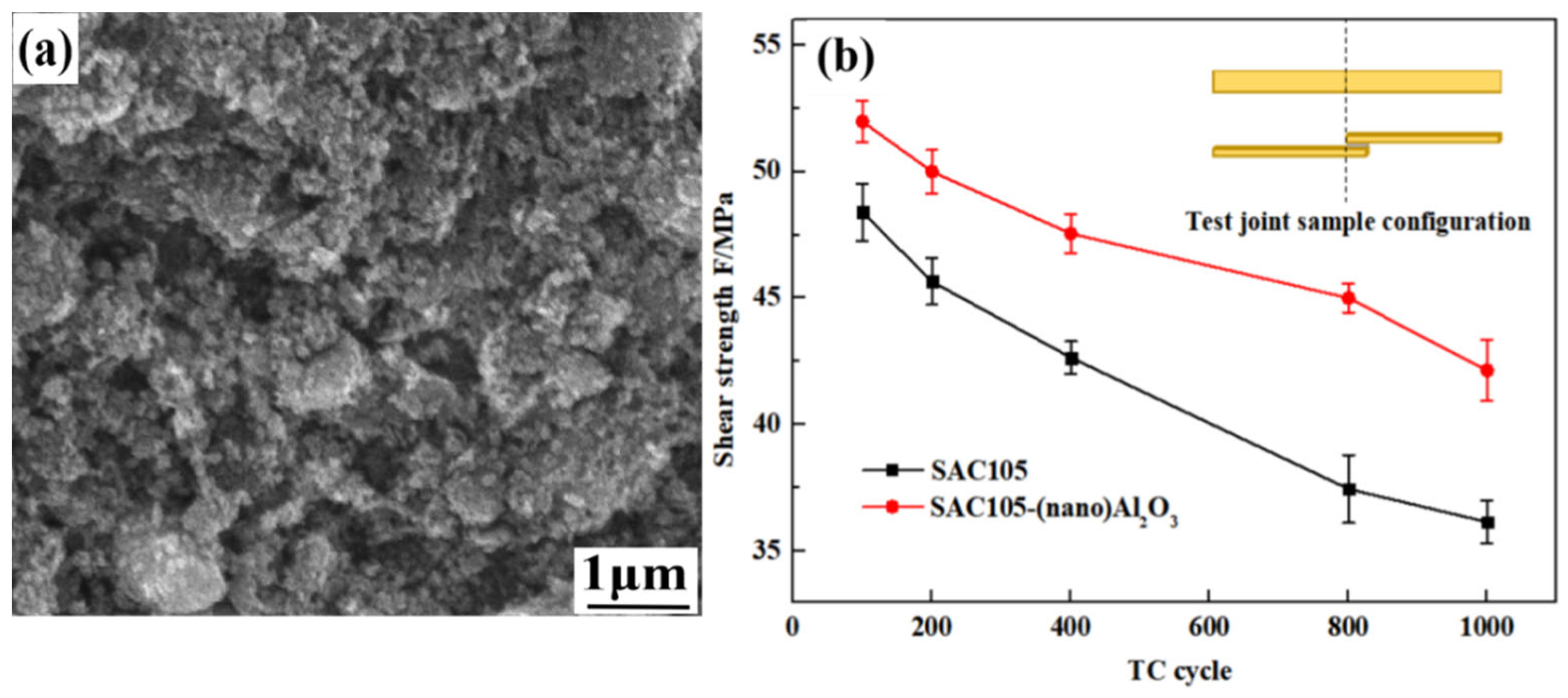
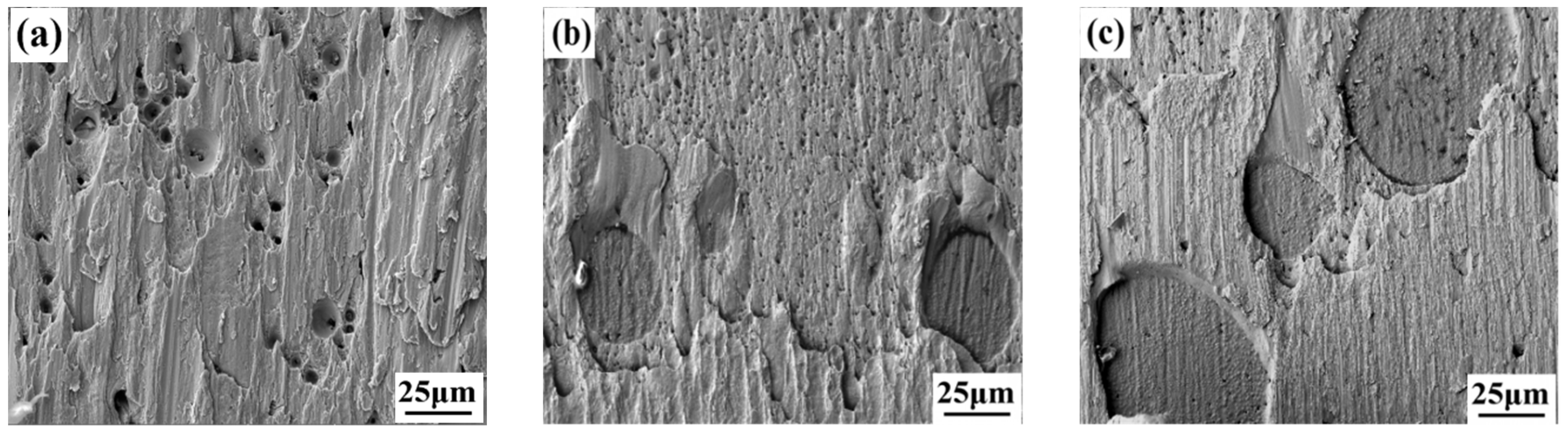
3.1. Shear Force and Fracture Morphology

Generally, a quick and convenient evaluation parameter for joint reliability is its shear strength. Figure 1b provided the shear strength of SAC105/Cu and SAC105-(nano)Al2O3/Cu solder joints during TC process. With TC number increased, the shear strength had degradation, but at a different rate. At the beginning, the decrease rate of shear strength of SAC105/Cu subjected to TC treatment was slower than that of nano-Al2O3 modified joint. However, as TC number increased from 800 to 1000, the decrease rate of SAC105-(nano)Al2O3/Cu (−6.3%) was higher than that of the original (−3.4%). This is probably due to the agglomeration of nano-Al2O3, which is hard and brittle and inducing micro-cracks. After 1000 TC number, the shear strength of SAC105/Cu and SAC105-(nano)Al2O3/Cu solder joints were 36.2 MPa and 42.1 MPa, respectively.
Figure 2 showed the fracture morphology of the joints after different TC numbers with shear loading to analyze the detailed fracture reasons. With first 100 cycles, the SAC105/Cu joint fractured with distinct elongated dimples, as shown in Figure 2a. Some dimples also formed on the surface with particles distributed at the bottom. With TC number increased to 400, the fracture surface became more superficial and two dark dimples with a relatively large size also emerged, which was inferred to be interfacial IMCs. Solder joints treated with 1000 TC number observed an IMC growth in the dark dimples. Figure 2d–f provided the SEM mapping images of elemental Sn (Figure 2d), Ag (Figure 2e), and Cu (Figure 2f) of the fracture morphology of SAC105/Cu joint treated with 1000 TC number. It was demonstrated that on the bottom of dark dimples were interfacial IMCs due to the enrichment distribution of elemental Sn and Cu. With nano-Al2O3 doped, the fracture morphology of composite solder joint observed a few dimples on the fracture surface, indicative an obvious characteristic of ductile fracture with micro-void accumulation. On the other hand, it suggested a higher shear strength than that of non-doped solder joint. With TC number increased, the dimple size increased with more distinct shearing trace (Figure 2h,i). It was noted that the bulk fractured Sn manifested layered phenomenon (marked with red arrow in Figure 2i), which was mainly caused by the embedded Al2O3 agglomerations, and corresponding to a rapid decrease in shear strength compared to that of the non-modified solder joint.

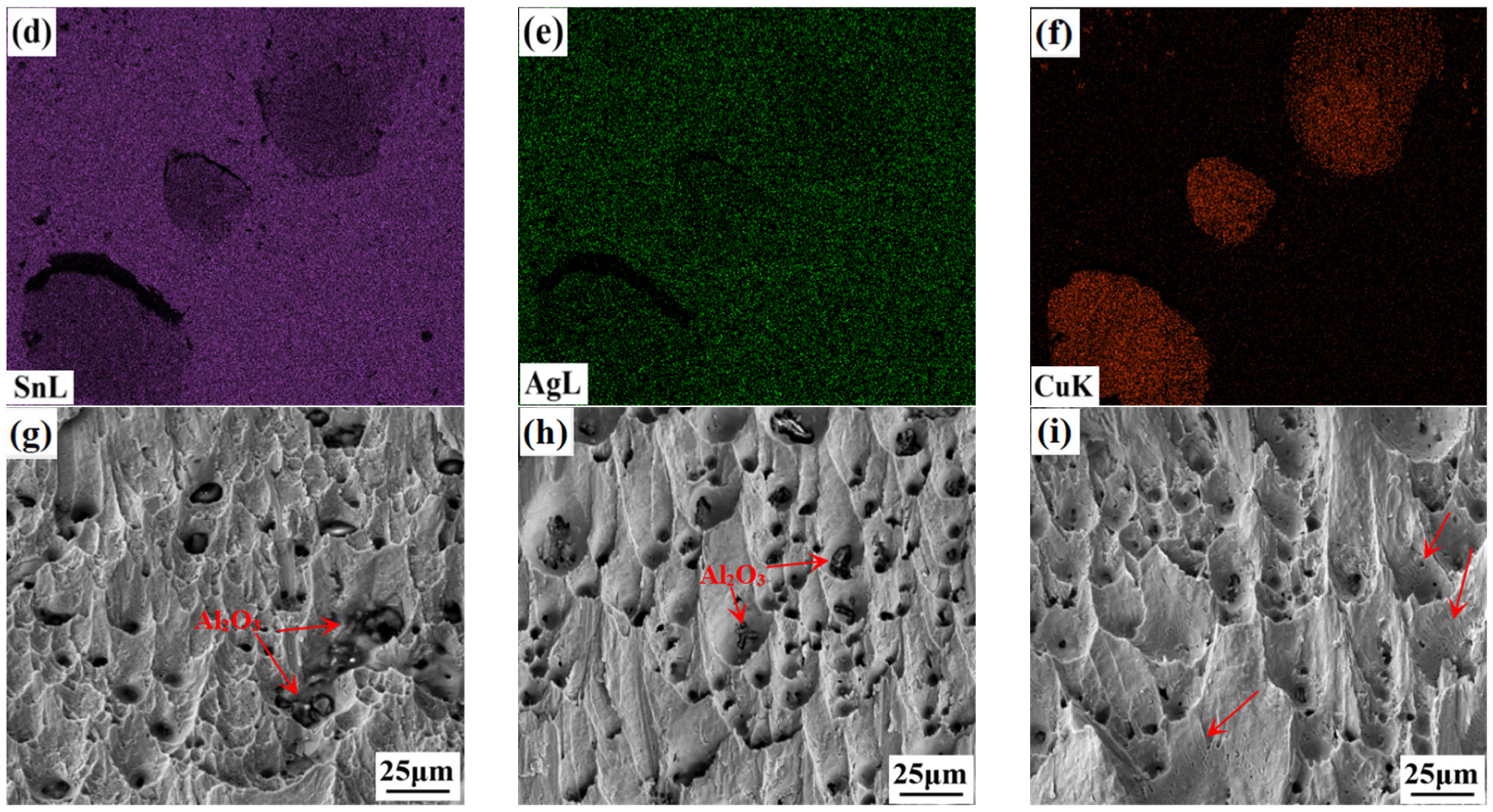
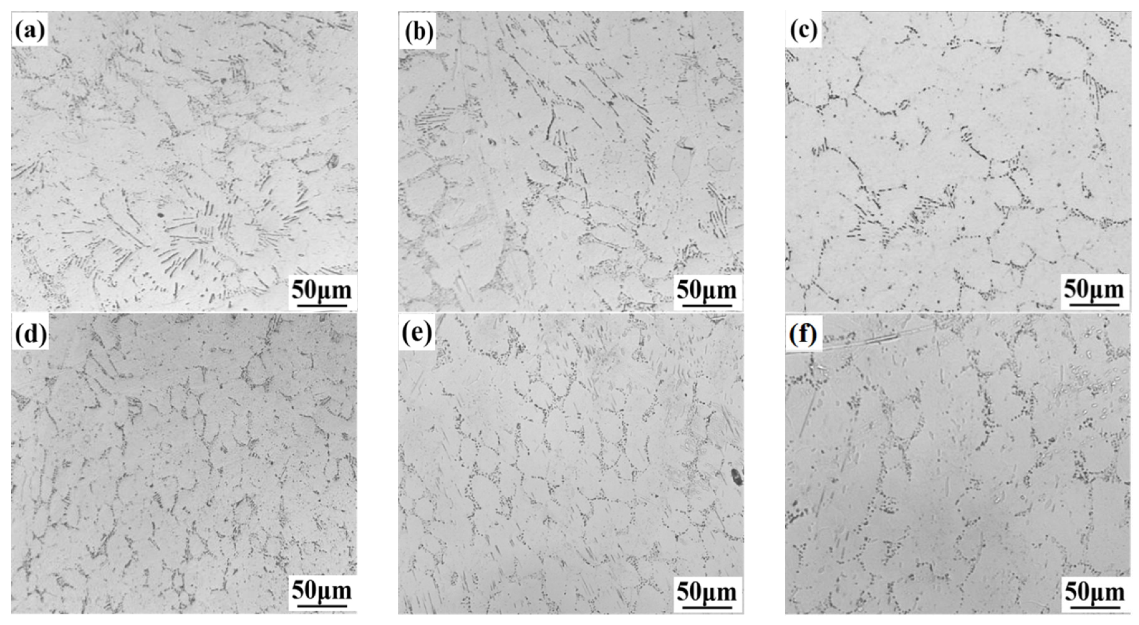
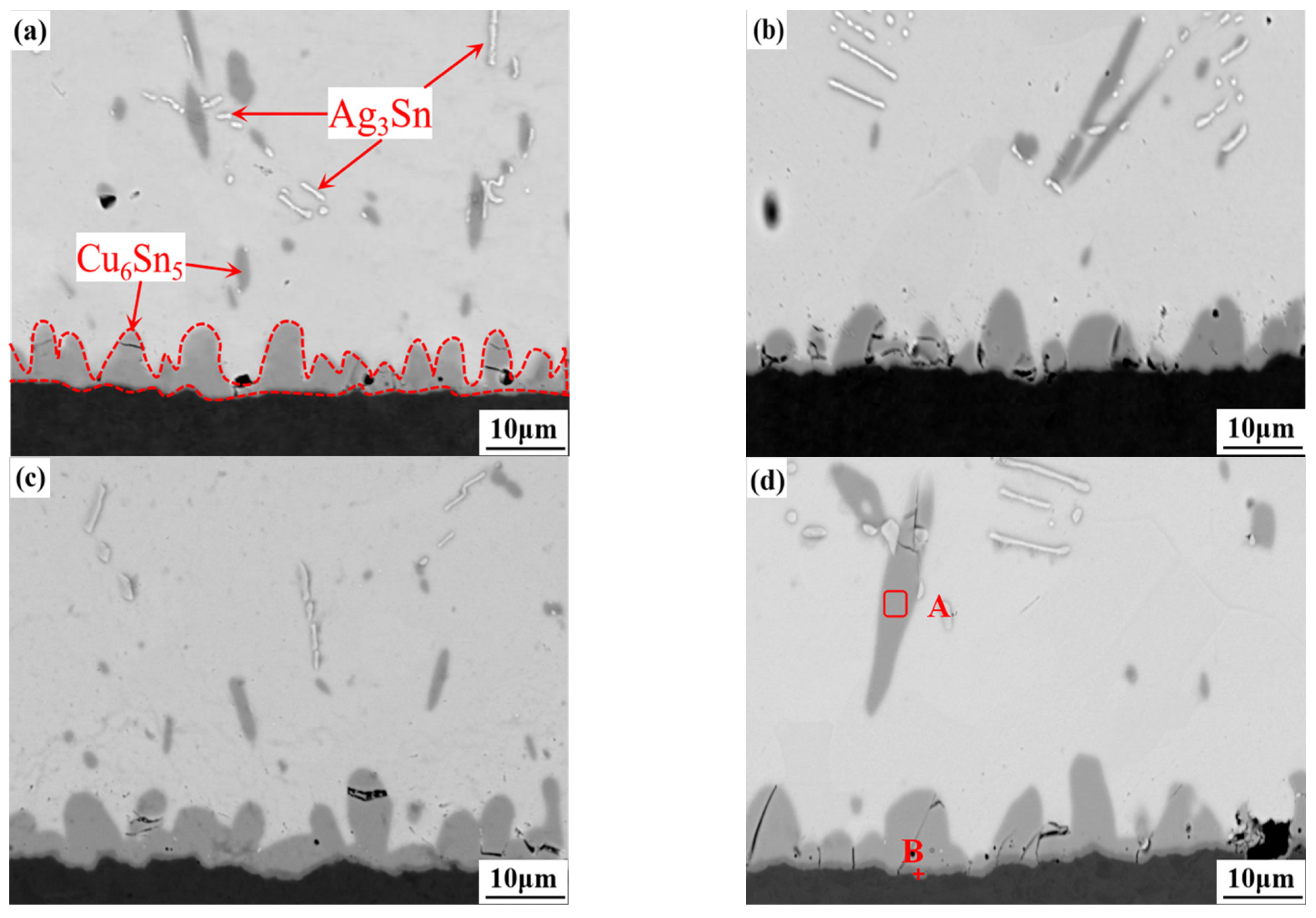
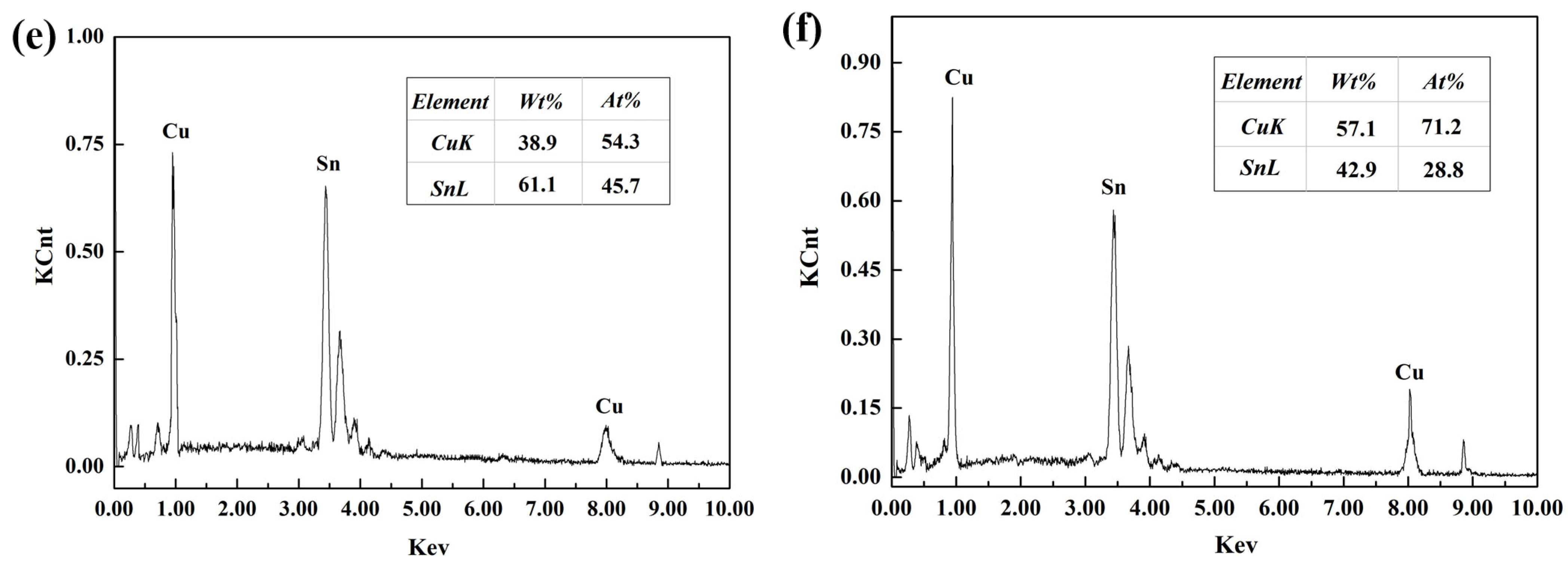
3.2. Interfacial Microstructure

The reliability is closely related with interfacial microstructure. Figure 3 shows the microstructures evolution of SAC105/Cu and SAC105-(nano)Al2O3/Cu solder joints subjected to TC treatment. Weather for SAC105/Cu or for SAC105-(nano)Al2O3/Cu solder joint, the bulk solder microstructure coarsened with β-Sn area increased and eutectic region becoming sparse. It led to a Sn dependency characteristic. It is clear that the microstructure of SAC105-(nano)Al2O3/Cu solder joint had a smaller coarsening rate, thus corresponding to a slower degradation in shear strength (Figure 3d–f). Even after 1000 TC number, the microstructure of SAC105-(nano)Al2O3/Cu solder joint was more refined than that of SAC105/Cu solder joint. It is attributed to the adsorption of nano-Al2O3 that can inhibit the grain growth during TC process.
Besides, morphologies of interfacial IMCs formed at the interfaces of SAC105/Cu and SAC105-(nano)Al2O3/Cu were provided in Figure 4 and Figure 5. It is clear that after 100 TC cycles, a scallop-like Cu6Sn5 IMCs [35] still displayed at the interface with few thin strip-shaped Ag3Sn IMCs [36] distributed (Figure 4a). With TC number increased, both sizes of interfacial IMCs and Ag3Sn had a further increase, and some micro-cracks began to emerge at the interface. In addition, the dark IMC layer, identified as Cu3Sn IMCs (Figure 4f) also formed at the interface, as shown in Figure 4b–d. With nano-Al2O3 doped, the growth of interfacial Cu6Sn5 IMCs was inhibited, manifested as a smaller thickness (Figure 5a). In addition, Ag3Sn IMCs also changed into particle-shaped, which were prone to distribute around Cu6Sn5 IMCs. Similarly, with TC number increased to 400, the growth of interfacial IMCs occurred. In addition, the inhibiting effect of Ag3Sn on Cu6Sn5 IMCs was also obvious, as shown in Figure 5b. An increase in TC number continues the growth of interfacial IMCs. Ag3Sn IMCs still maintained nano-scaled (Figure 5c), which grew into a micro scale with the TC number increased to 1000 (Figure 5d). Further, a few Ag3Sn IMCs, demonstrated by EDS analysis shown in Figure 5e, also formed at the interfacial IMCs due to a short diffusion pathway at the boundary than at the interfacial IMC top. It played a role as a pinning effect on IMCs merging. Figure 6a provided the detailed distributed illustration of nano-scaled Ag3Sn and Al2O3. Clearly, the nano-scaled Ag3Sn and Al2O3 tended to adsorbed at the grain surfaces or boundaries, and pinning the IMCs growth.

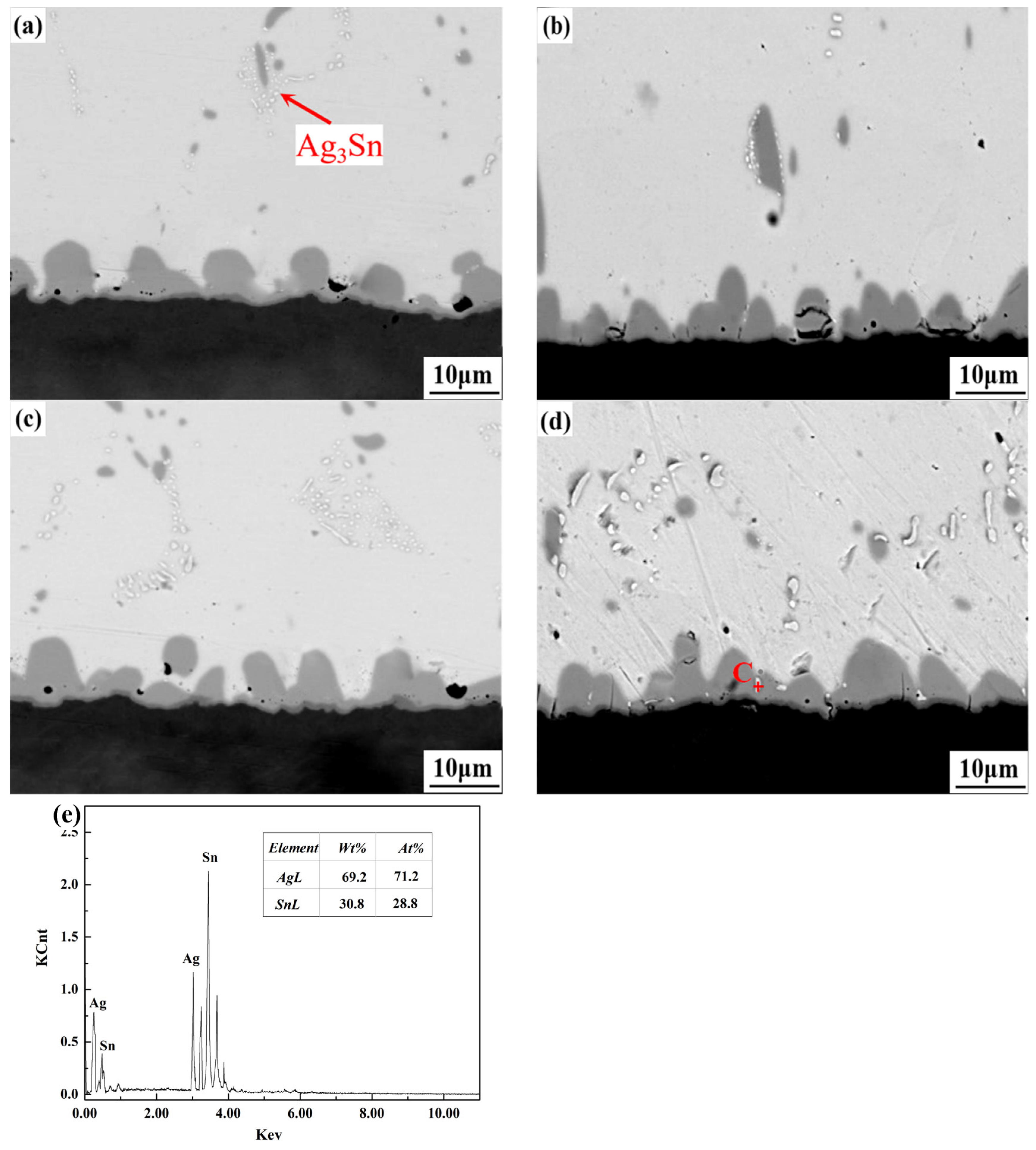
3.3. Interfacial IMC Growth Kinetics

Due to the diffusion barrier of nano-Al2O3, the SAC105-(nano)Al2O3/Cu interface exhibited a slower growth in interfacial IMCs. Hence, it is essential to study the interfacial IMC growth kinetics to quantify the inhibition effect. During the high temperature stage of one TC number, interfacial IMCs had a solid-solid reaction contributed by Cu diffusion from Cu substrate. With first 100 TC number, the thickness of interfacial IMCs at SAC105/Cu and SAC105-(nano)Al2O3/Cu approached ~5.2 and ~3.8 μm, respectively. As the TC number increased to 1000, the interfacial IMC thickness of SAC105-(nano)Al2O3/Cu reached ~5.5 μm, about 23.6% thinner than that of SAC105/Cu solder joint. A detailed interfacial IMC thickness change at SAC105/Cu and SAC105-Al2O3/Cu interface was provided in Figure 6b. Considering a solid-solid reaction, the classic diffusion mode was used to describe the process [37]:
l t = l 0 + D ¯ t
where l t represents the thickness of interfacial IMCs after time t, l 0 is the initial IMC thickness, D ¯ is the average diffusion coefficient. It can be calculated from the slope of interfacial IMC thickness—time/cycle curve.
Hence, a relationship between the thickness of interfacial IMC layer and the TC time t was plotted in Figure 6. The final fitted equations displayed as follows:
l SAC 105 = 4.26 + 0.092 × t
l SAC 105 nano Al 2 O 3 = 2.96 + 0.081 × t
It was clear that nano-Al2O3 modified solder has a relatively lower average growth coefficient, which was calculated to be 6.5 × 10⁻¹¹ cm2/h, about 22.6% lower than that if original solder joint (8.4 × 10⁻¹¹ cm2/h). This is mainly related to the pinning effect of nano-Al2O3 on the growth of interfacial IMCs.

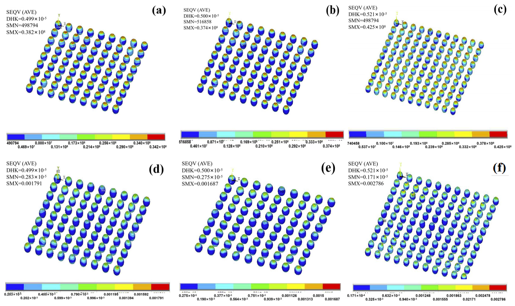
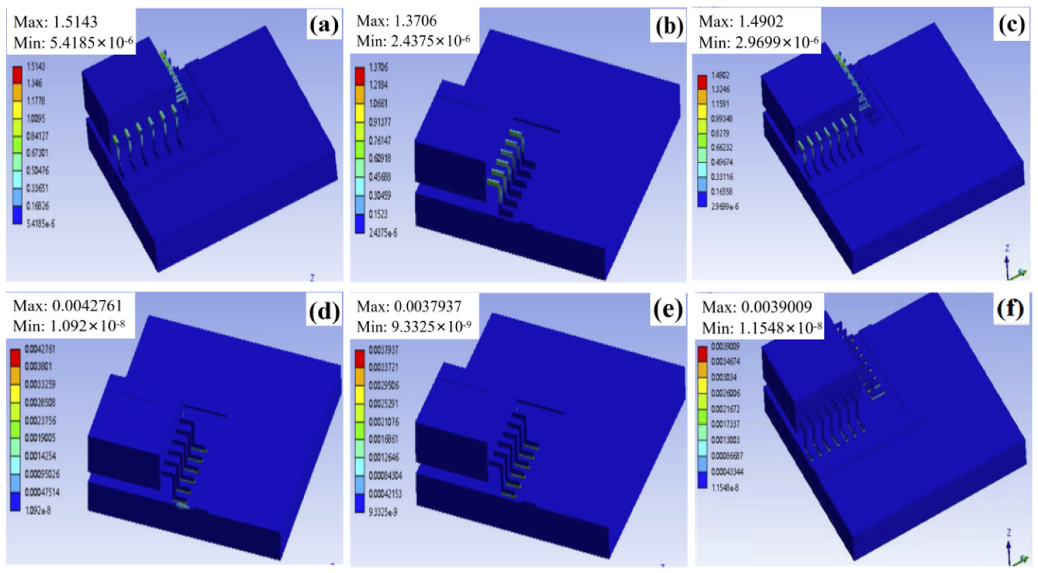
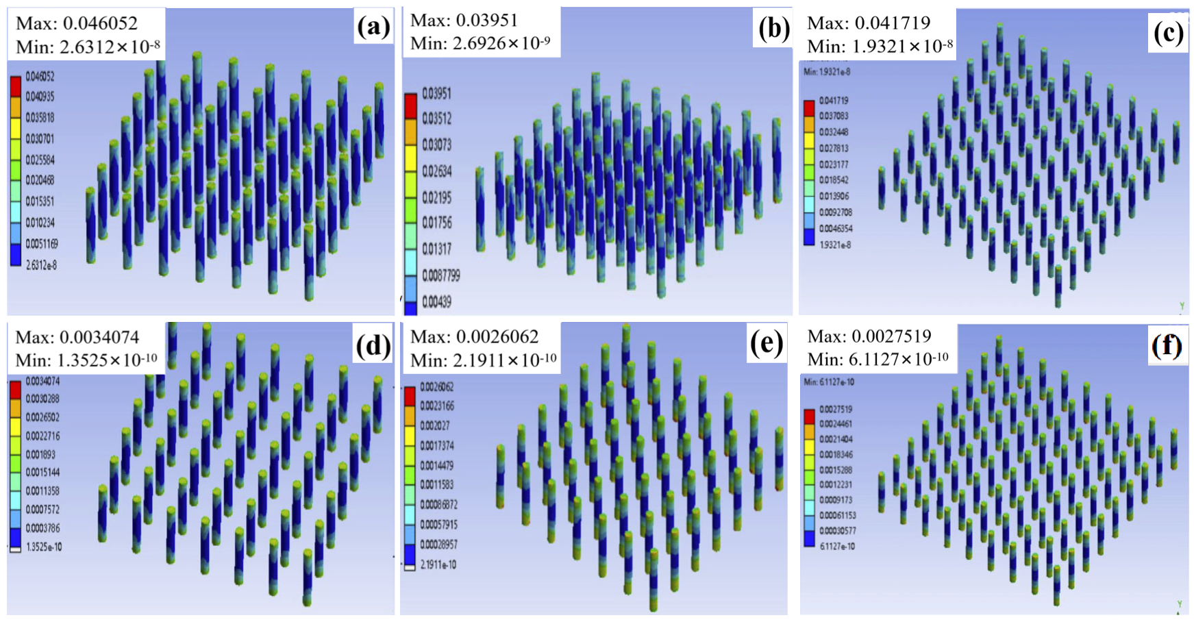
3.4. Application in High-Density Electronic Packaging

In order to promote the nano-Al2O3 modified solder into the electronic market, its application in high-density packaging should be attempted. Before then, it is essential to make a Finite Element simulation to predict detailed behaviors of high-density solder joints under TC treatment in advance. Hence, three mainstream packaging forms (QFP, BGA and CCGA) are selected to build three-dimensional Finite Element model of electronic packaging structure loaded with TC. Corresponding stress and strain distribution was simulated.
Figure 7, Figure 8 and Figure 9 shows the detailed TC simulation results of BGA80A, QFP48, and CCGA575 using different solders and with different arrays. For BGA80A, it can be seen from the stress and strain distribution cloud diagram (Figure 7) that both stress and strain concentrated on the top side of the balls, and decreased in the height direction. With trace addition of nano-Al2O3, the average stress and strain of solder ball was relieved (Figure 7b,e). With solder ball array increased from 9 × 9 to 11 × 11, the location of stress and strain was unchanged, while the stress had a small increment, which was not that considerable compared to the original (Figure 7c,f). Figure 8 showed the FEM stress (Figure 8a–c) and strain (Figure 8d–f) analyzed results of QFP48 electronic packaging subjected to TC. It was clear that the contributed stress mainly concentrated on the pin and chip connection part, while the pin and substrate connection part had a relatively obvious strain concentration. When the nano-Al2O3 modified solder was used, the maximum stress and strain were decreased from 1.5143 to 1.3706, from 0.0042761 to 0.0037937, respectively. With the number of pins increased to 4 × 14, both stress and strain had a small increase when compared to the QFP48 packaging using the nano-Al2O3 modified solder, but still smaller than the non-modified solder. For CCGA575 electronic packaging, FEM analysis results presented a stress and strain distribution at both connection ends. With the application of nano-Al2O3 modified solder, both the maximum stress and strain had a decrease. With bonding array increased to 11 × 11, the maximum stress and strain was also slightly increased, but still lower than that of the packaging using SAC105 solder with 9 × 9 array.
It can be concluded that the application of using nano-Al2O3 modified solder can effectively undertake partial stress and strain during TC treatment, contributing to a decreased stress and strain distribution even with increasing the packaging arrays of QFP and CCGA. Hence, it has great potential for nano-Al2O3 modified solder to be used in high-density electronic packaging. However, abundant experimental work still remains to be done to demonstrate it in the future.

4. Conclusions

In this study, the TC reliability of nano-Al2O3 modified SAC105 low-Ag solder joint was investigated, and its possibility application in high-density electronic packaging was explored with FEM analysis. Detailed conclusions were drawn as follows:
1.
With nano-Al2O3 particles doped, the TC reliability of SAC105 low-Ag solder joint was enhanced, manifesting as a slower degradation in joint mechanical strength when compared to the non-modified joint. Corresponding fracture morphology also showed that SAC105-(nano)Al2O3/Cu always presented a typical ductile fracture with micro-void accumulation fracture mode.
2.
The enhanced TC reliability is mainly attributed to the insoluble Al2O3 NPs absorbing on the grain surface, inhibiting the microstructure coarsening. In addition, some nano-scaled Ag3Sn particles also tended to form at the phase boundary, and contributing to decreasing the IMC coarsening rate in bulk solder.
3.
Doping of nano-Al2O3 exerted a pinning effect on the interfacial IMCs due to their absorption on grain surfaces of interfacial IMCs. Thus, the flux of Cu dissolution from Cu substrate via GB channels was decreased, representing a suppressed growth of interfacial IMCs. Theoretical calculation also demonstrated a decrease in the average growth coefficients of interfacial IMCs, from 8.4 × 10⁻¹¹ cm2/h to 6.5 × 10⁻¹¹ cm2/h.
4.
From the FEM simulation results of applying nano-Al2O3 modified solder in high-density packaging, it was clear that the induced stress and strain with TC treatment can be decreased. However, as the TC number increased, the induced stress and strain slightly increased, which was still not much more severe than that of the non-modified one.

Author Contributions

Conceptualization: J.W.; Methodology: J.W., G.H.; FEM analysis and investigation: X.H., R.Y., Y.W.; Data curation: X.Y., G.C.; Writing—original draft preparation: J.W.; Writing—review and editing: G.H., C.T., Z.Y.; Funding acquisition: J.W., H.S., Y.X.; Supervision: G.H., Y.X. All authors have read and agreed to the published version of the manuscript.

Funding

This work was financially supported by [National Natural Science Foundation of China], Grant number [52105369], [12004194], [52205436]. In addition, it was founded by [Natural Science Foundation of the Jiangsu Higher Education Institutions of China], Grant number [20KJB460008]; the [Natural Science Foundation of Jiangsu Province] Grant number [BK20200746], [BK20180759]; the [China Postdoctoral Science Foundation], Grant number [2021M693581]; and [Starting founding from Nanjing University of Posts and Telecommunications] (NJUPTSF), Grant number [NY220077], and [NY220066]. Also, it was also founded by [Guangdong Province Research and Development in Key Fields from Guangdong Greater Bay Area Institute of Integrated Circuit and System], Grant number [2021B0101280002] and [Guangzhou City Research and Development Program in Key Field], Grant number [20210302001] also support the work.

Institutional Review Board Statement

Not applicable.

Informed Consent Statement

Not applicable.

Data Availability Statement

This study does not contain any studies with human participants or animals performed by any of the authors.

Conflicts of Interest

The authors declare no conflict of interest.

References

  1. Chen, R.; Li, Y.C.; Cai, J.M.; Cao, K.; Lee, H.B.R. Atomic level deposition to extend Moore’s law and beyond. Int. J. Extrem. Manuf. 2020, 2, 022002. [Google Scholar] [CrossRef]
  2. Lu, N.; Yang, D.; Li, L. Interfacial reaction between Sn–Ag–Cu solder and Co–P films with various microstructures. Acta Mater. 2013, 61, 4581–4590. [Google Scholar] [CrossRef]
  3. Ajayan, J.; Nirmal, D.; Tayal, S.; Bhattacharya, S.; Arivazhagan, L.; Fletcher, A.A.; Murugapandiyan, P.; Ajitha, D. Nanosheet field effect transistors—A next generation device to keep Moore’s law alive: An intensive study. Microelectron. J. 2021, 114, 105141. [Google Scholar] [CrossRef]
  4. Hao, Y.; Wu, H.; Yang, Y.; Liu, Q.; Gong, X.; Han, G.; Li, M. Preface to the Special Issue on Beyond Moore: Three-Dimensional (3D) Heterogeneous Integration. J. Semicond. 2021, 42, 020101. [Google Scholar] [CrossRef]
  5. Chou, T.-T.; Song, R.-W.; Chen, H.; Duh, J.-G. Low thermal budget bonding for 3D-package by collapse-free hybrid solder. Mater. Chem. Phys. 2019, 238, 121887. [Google Scholar] [CrossRef]
  6. Spurney, R.G.; Sharma, H.; Raj, P.M.; Tummala, R.; Lollis, N.; Weaver, M.; Romig, M.; Gandhi, S.; Brumm, H. 3-D Packaging and Integration of High-Density Tantalum Capacitors on Silicon. IEEE Trans. Compon. Packag. Manuf. Technol. 2019, 9, 1466–1472. [Google Scholar] [CrossRef]
  7. Lu, M.C. Advancement of Chip Stacking Architectures and Interconnect Technologies for Image Sensors. J. Electron. Packag. 2022, 144, 020801. [Google Scholar] [CrossRef]
  8. Liu, X.; Chen, Y.; Li, J.; Qiao, Y.; Ma, Q.; Shan, S.; Zhang, H.; Tang, X. Failure Analysis Technology for High Density Packaging and Its Application. Semicond. Technol. 2018, 43, 310–315. [Google Scholar]
  9. Liu, M.; Nie, J.; Liu, Y.; Sun, J.; Li, M.; Yan, C.; Yan, Q. Research on the reliability of Micro LED high-density solder joints under thermal cycling conditions. J. Phys. Conf. Ser. 2022, 2221, 012010. [Google Scholar] [CrossRef]
  10. Zhang, L.; Tu, K.N. Structure and properties of lead-free solders bearing micro and naXno particles. Mater. Sci. Eng. R 2014, 82, 1–32. [Google Scholar] [CrossRef]
  11. Li, M.L.; Gao, L.L.; Zhang, L.; Long, W.M.; Zhong, S.J.; Zhang, L. Interfacial evolution of pure Sn solder bearing silicon carbide nanowires under isothermal aging and thermal cycling. J. Mater. Res. Technol. 2021, 15, 3974–3982. [Google Scholar] [CrossRef]
  12. Gu, T.H.; Xu, Y.L.; Gourlay, C.M.; Britton, T.B. In-situ electron backscatter diffraction of thermal cycling in a single grain Cu/Sn-3Ag-0.5Cu/Cu solder joint. Scr. Mater. 2020, 175, 55–60. [Google Scholar] [CrossRef]
  13. Wang, J.H.; Xue, S.B.; Liu, L.; Zhang, P.; Nishikawa, H. Three-dimensional interface and property of SnPb solder joint under extreme thermal shocking. Sci. Technol. Weld. Join. 2022, 27, 186–196. [Google Scholar] [CrossRef]
  14. Sun, L.; Zhang, L.; Zhong, S.J.; Ma, J.; Bao, L. Reliability Studies of Sn-3.0Ag-0.5Cu Solder Joints. Electron. Process Technol. 2015, 36, 187. [Google Scholar]
  15. Zhang, S.; Duan, R.; Xu, S.; Xue, P.; Wang, C.; Chen, J.; Paik, K.W.; He, P. Shear performance and accelerated reliability of solder interconnects for fan-out wafer-level package. J. Adv. Join Process. 2022, 5, 100076. [Google Scholar] [CrossRef]
  16. Wang, Y.; Zhao, X.C.; Liu, Y.; Wang, Y.; Li, D.M. Microstructure, wetting property of Sn–Ag–Cu–Bi–xCe solder and IMC growth at solder/Cu interface during thermal cycling. Rare Met. 2021, 40, 714–719. [Google Scholar] [CrossRef]
  17. Tikale, S.; Prabhu, K.N. Development of low-silver content SAC0307 solder alloy with Al2O3 nanoparticles. Mater. Sci. Eng. A 2020, 787, 139439. [Google Scholar] [CrossRef]
  18. Liu, L.; Shi, L.; Peng, J.; Jiang, B.; Liu, S.; Liu, C.; Chen, Z. Interfacial reaction between Sn-Ag solder and electroless Ni-Fe-P diffusion barriers with different internal microstructure. Mater. Res. Bull. 2022, 152, 111854. [Google Scholar] [CrossRef]
  19. Muhamad, M.; Masri, M.N.; Nazeri, M.F.M.; Mohamad, A.A. The Effect of Bismuth Addition on Sn-Ag-Cu Lead-Free Solder Properties: A Short Review. IOP Conf. Ser. Earth Environ. Sci. 2020, 596, 012007. [Google Scholar] [CrossRef]
  20. El-Daly, A.; El-Hosainy, H.; Elmosalami, T.; Desoky, W. Microstructural modifications and properties of low-Ag-content Sn–Ag–Cu solder joints induced by Zn alloying. J. Alloys Compd. 2015, 653, 402–410. [Google Scholar] [CrossRef]
  21. Wu, J.; Xue, S.; Huang, G.; Sun, H.; Chi, F.; Yang, X.; Xu, Y. In-situ synergistic effect of Pr and Al2O3 nanoparticles on enhancing thermal cycling reliability of Sn-0.3 Ag-0.7 Cu/Cu solder joint. J. Alloys Compd. 2022, 905, 164152. [Google Scholar] [CrossRef]
  22. Shnawah, D.A.; Sabri, M.F.M.; Badruddin, I.A.; Said, S.B.M.; Bashir, M.B.A.; Sharif, N.M.; Elsheikh, M.H. Study on coarsening of Ag3Sn intermetallic compound in the Fe-modified Sn–1Ag–0.5Cu solder alloys. J. Alloys Compd. 2015, 622, 184–188. [Google Scholar] [CrossRef]
  23. Liu, P.; Gu, X.L.; Zhong, H.F.; Jin, X.; Zhe, J. New Brazing Material and vacuum brazing: Study on novel low-Ag solder SAC0307X. Electron. Compon. Mater. 2015, 34, 129–133. [Google Scholar]
  24. Yang, M.; Ji, H.; Wang, S.; Ko, Y.H.; Lee, C.W.; Wu, J.; Li, M. Effects of Ag content on the interfacial reactions between liquid Sn–Ag–Cu solders and Cu substrates during soldering. J. Alloys Compd. 2016, 679, 18–25. [Google Scholar] [CrossRef]
  25. Illés, B.; Choi, H.; Hurtony, T.; Skwarek, A.; Dusek, K.; Busek, D. Suppression of Sn whisker growth from SnAgCu solder alloy with TiO2 and ZnO reinforcement nano-particles by increasing the corrosion resistance of the composite alloy. J. Mater. Res. Technol. 2022, 20, 4231–4240. [Google Scholar] [CrossRef]
  26. Sayyadi, R.; Khodabakhshi, F.; Javid, N.S.; Khatibi, G. Influence of graphene content and nickel decoration on the microstructural and mechanical characteristics of the Cu/Sn–Ag–Cu/Cu soldered joint. J. Mater. Res. Technol. 2020, 9, 8953–8970. [Google Scholar] [CrossRef]
  27. Xu, L.; Wang, L.; Jing, H.; Liu, X.; Wei, J.; Han, Y. Effects of graphene nanosheets on interfacial reaction of Sn-Ag-Cu solder joints. J. Alloys Compd. 2015, 650, 475–481. [Google Scholar] [CrossRef]
  28. Skwarek, A.; Krammer, O.; Hurtony, T.; Ptak, P.; Górecki, K.; Wroński, S.; Straubinger, D.; Witek, K.; Illés, B. Application of ZnO nanoparticles in Sn99Ag0.3Cu0.7 based composite solder alloys. Nanomaterials 2021, 11, 1545. [Google Scholar] [CrossRef] [PubMed]
  29. Xing, W.Q.; Yu, X.Y.; Li, H.; Ma, L.; Zuo, W.; Dong, P.; Wang, W.X.; Ding, M. Effect of nano-Al2O3 additions on the interfacial behavior and mechanical properties of eutectic Sn-9Zn solder on low temperature wetting and soldering of 6061 aluminum alloys. J. Alloys Compd. 2016, 695, 574–582. [Google Scholar] [CrossRef]
  30. Tsao, L.C.; Wu, R.W.; Cheng, T.H.; Fan, K.H.; Chen, R.S. Effects of nano-Al2O3 particles on microstructure and mechanical properties of Sn3.5Ag0.5Cu composite solder ball grid array joints on Sn/Cu pads. Mater. Des. 2013, 50, 774–781. [Google Scholar] [CrossRef]
  31. Tikale, S.; Prabhu, K.N. Performance and reliability of Al2O3 nanoparticles doped multicomponent Sn-3.0Ag-0.5Cu-Ni-Ge solder alloy. Microelectron. Reliab. 2020, 113, 113933. [Google Scholar] [CrossRef]
  32. Zhang, Y.; Madenci, E.; Zhang, Q. ANSYS implementation of a coupled 3D peridynamic and finite element analysis for crack propagation under quasi-static loading. Eng. Fract. Mech. 2022, 260, 108179. [Google Scholar] [CrossRef]
  33. Bai, T.; Qiao, Y.; Wang, X.; Zhao, N. Finite element method modeling of temperature gradient-induced Cu atomic thermomigration in Cu/Sn/Cu micro solder joint. Microelectron. Reliab. 2022, 129, 114479. [Google Scholar] [CrossRef]
  34. Xie, M.W.; Chen, G.; Yu, J.T.; Wu, Y.; Liu, X.; Yang, J.; Xu, W.L. A dual-phase crystal plasticity finite-element method for modeling the uniaxial deformation behaviors of thermally aged SAC305 solder. Int. J. Plast. 2022, 155, 103342. [Google Scholar] [CrossRef]
  35. Qiao, Y.Y.; Ma, H.T.; Yu, F.Y.; Zhao, N. Quasi-in-situ observation on diffusion anisotropy dominated asymmetrical growth of Cu-Sn IMCs under temperature gradient. Acta Mater. 2021, 217, 117168. [Google Scholar] [CrossRef]
  36. Qiao, C.; Sun, X.; Wang, Y.Z.; Hao, L.; An, X.Z. A perspective on effect by Ag addition to corrosion evolution of Pb-free Sn solder. Mater. Lett. 2021, 297, 129935. [Google Scholar] [CrossRef]
  37. Tu, K.N.; Liu, Y. Recent advances on kinetic analysis of solder joint reactions in 3D IC packaging technology. Mater. Sci. Eng. R Rep. 2019, 136, 1–12. [Google Scholar] [CrossRef]
Figure 1. (a) SEM image of Al2O3 nanoparticles; (b) Changes in shear strengths of SAC105/Cu and SAC105-(nano)Al2O3/Cu solder joints.
Crystals 12 01736 g001
Figure 2. SEM micrograph of fracture morphology of SAC105/Cu (ac) and SAC105-(nano)Al2O3/Cu (gi) solder joint subjected to: 100 cycle (a,g); 400 cycle (b,h); 1000 cycle (c,i); Mapping image of elemental Sn: (d), Ag: (e), and Cu: (f).
Crystals 12 01736 g002aCrystals 12 01736 g002b
Figure 3. Microstructure images of SAC105/Cu: (ac) and SAC105-(nano)Al2O3/Cu: (df) subjected to 100 cycle: (a,d); 400 cycle: (b,e); 1000 cycle: (c,f).
Crystals 12 01736 g003
Figure 4. Interfacial microstructure of SAC105/Cu solder joint subjected to (a) 100 cycle; (b) 400 cycle; (c) 800 cycle; (d) 1000 cycle; (e) EDS analysis of area A in (d); (f) EDS analysis of point B in (d).
Crystals 12 01736 g004aCrystals 12 01736 g004b
Figure 5. Interfacial microstructure of SAC105-(nano)Al2O3/Cu solder joint subjected to (a) 100 cycle; (b) 400 cycle; (c) 800 cycle; (d) 1000 cycle; (e) EDS analysis of point C.
Crystals 12 01736 g005
Figure 6. (a) Distributed illustration of nano-Al2O3 and Ag3Sn IMCs; (b) Thickness of the interfacial IMCs at SAC105/Cu and SAC105-(nano)Al2O3/Cu interface subjected to TC.
Crystals 12 01736 g006
Figure 7. FEM analysis of stress (ac) and strain (df) analysis of BGA80A electronic packaging subjected to TC: 9 × 9, SAC105: (a,d); 9 × 9, SAC105-(nano)Al2O3/Cu: (b,e); 11 × 11, SAC105-(nano)Al2O3/Cu: (c,f).
Crystals 12 01736 g007
Figure 8. FEM analysis of stress (ac) and strain (df) analysis of QFP48 electronic packaging subjected to TC: 4 × 12, SAC105: (a,d); 4 × 12, SAC105-(nano)Al2O3/Cu: (b,e); 4 × 14, SAC105-(nano)Al2O3/Cu: (c,f).
Crystals 12 01736 g008
Figure 9. FEM analysis of stress (ac) and strain (df) analysis of CCGA575 electronic packaging subjected to TC: 9 × 9, SAC105: (a,d); 9 × 9, SAC105-(nano)Al2O3/Cu: (b,e); 11 × 11, SAC105-(nano)Al2O3/Cu: (c,f).
Crystals 12 01736 g009
Table 1. Samples with different analysis technique.
Analysis TechniqueBrandTest Sample
Drying boxDZF-6050-220V-MS, Hefei Kejing Material Technology Co., Ltd., Hefei, ChinaAl2O3 NPs
Automatic solder paste mixerZB500S, Huaqi Zhengbang Co., Ltd., Zhejiang, ChinaSolder paste
Thermal shock test chamberCJ61S2, Chongqing Yinhe Test Instrument Co., Ltd., Chongqing, Chinalap-shaped joint sample
Tensile testing machineWEW-100B, Jinan Liling Testing Machine Co., Ltd., Jinan, Chinalap-shaped joint sample subjected with different TC cycles (100, 200, 400, 800, 1000)
FE-SEMTescan Mira3solder joint sample subjected with different TC cycle (100, 200, 400, 800, 1000)
EDSBruker, Billerica, MA, USAsolder joint sample subjected with different TC cycles (100, 200, 400, 800, 1000)
Publisher’s Note: MDPI stays neutral with regard to jurisdictional claims in published maps and institutional affiliations.

