Article

Epitaxial Lateral Overgrowth of {11-22} InGaN Layers Using Patterned InGaN Template and Improvement of Optical Properties from Multiple Quantum Wells

Yamaguchi University, 2-16-1 Tokiwadai Ube, Yamaguchi 755-8611, Japan
*
Author to whom correspondence should be addressed.
Crystals 2022, 12(10), 1373; https://doi.org/10.3390/cryst12101373
Submission received: 27 July 2022 / Revised: 23 September 2022 / Accepted: 25 September 2022 / Published: 27 September 2022
(This article belongs to the Special Issue III-Nitride-Based Light-Emitting Devices)

Abstract

:
We report the growth and characterization of thick, completely relaxed {11-22}-oriented InGaN layers using epitaxial lateral overgrowth (ELO). Although it was difficult to grow ELO-InGaN layers on patterned GaN templates, we succeeded in growing ELO-InGaN layers on a patterned InGaN template. The full width at half maximum of the X-ray rocking curve of ELO-InGaN on the InGaN templates was less than that of non-ELO InGaN. The photoluminescence intensity of InGaN/GaN multiple quantum wells on ELO-InGaN was approximately five times stronger than that on the {11-22} GaN template.

1. Introduction

Light-emitting diodes (LEDs) with very high external quantum efficiencies (EQEs) have been developed based on advancements in LED fabrication technologies. The EQEs of LEDs with different wavelengths in the visible light region (from purple to red) have been improved, with record efficiencies being reported [1,2,3,4,5]. There has also been an increasing demand for laser diodes (LDs) with longer emission wavelengths [6]. In particular, GaN-based LEDs have attracted increasing attention as promising materials for optoelectronic device applications. InGaN-based multiple quantum wells (MQWs) are typically used as an active layer in such devices and are grown on a thick GaN template layer or a GaN substrate. However, the major factors that prevent the realization of high-performance devices are the large internal electric field [7] and the generation of misfit dislocations caused by the large lattice mismatch between the GaN template and InGaN active layer [8]. One of the most promising routes for realizing high-efficiency, longer-wavelength LEDs and LDs based on InGaN is the use of a thick underlying layer composed of an InGaN ternary alloy with a low defect density that can reduce the lattice mismatch between the template and active layer. For this reason, the fabrication of thick c-plane InGaN layers has been of considerable interest [9,10,11,12]. In addition, the relaxation effects of InGaN [13,14,15] and pseudomorphic InGaN layers [16] have been reported. However, the crystalline quality of the InGaN layers currently produced is insufficient for the above purpose. Furthermore, from the viewpoint of the fabrication of high-quality InGaN layers grown on GaN, the c-plane is not suitable. This is because a very rough surface with a high dislocation density, consisting of {10-11} or {11-22} planes, is formed after the relaxation of the InGaN layer grown on the c-plane of GaN. The growth of the InGaN layer on the {10-11} or {11-22} planes is a potential solution to this problem because these planes are stable at lower growth temperatures [17]. In addition, they are stable after relaxation, where the relaxation mechanism of these planes was reported by Tyagi et al [18]. However, the generation of misfit dislocations is a crucial setback when nonpolar or semipolar planes similar to the c-plane are used because of the large lattice mismatch between GaN and InGaN [19,20]. Epitaxial lateral overgrowth (ELO) on {10-11} or {11-22} surfaces has emerged as a promising technique for preparing the InGaN layers required for the above-mentioned applications. There are very few studies reporting the ELO of InGaN, for example, on the m-plane InGaN layer [21,22]. Therefore, it is important to investigate the ELO of {10-11}- or {11-22}-oriented InGaN layers in order to understand the growth mechanism of InGaN. In recent years, many researchers have explored red LEDs using a relaxed [9,10,23,24] or semi-relaxed [25,26] InGaN underlayer on the GaN or coherent InGaN underlayer using a ScAlMgO4 substrate [27]. In particular, nitride-based red LEDs have attracted much attention for micro-LEDs [28,29,30]. The EQE of nitride-based red LEDs is significantly lower than those of the blue and green LEDs; the highest EQE of red LED is 4.5% [1,3,31]. Previously, EQEs of 1% and 3% were obtained by Eu doping and using InGaN underlayers, respectively [32,33]. The efficiency of red LEDs is gradually increasing, but further improvement is still needed. The requirements for a relaxed InGaN indicate that it is also important to investigate the potential of a relaxed nonpolar or semipolar InGaN template.
In this study, we focused on the growth of {11-22} InGaN layers as templates to incorporate the InGaN MQWs, which, in turn, were used to fabricate LEDs. We report the growth of a completely relaxed and thick {11-22}-oriented InGaN layer with a high crystalline quality and a smooth surface using the ELO method for use as a thick underlying layer.

2. Experimental Methods

A semipolar {11-22} GaN template on an m-plane sapphire substrate was prepared. The GaN layer was grown on the m-plane sapphire substrate by the hydride vapor phase epitaxy. Ammonia (NH3) and GaCl, mixed with purified H2 and N2 carrier gases, were used as the nitrogen and gallium sources, respectively. The reactor pressure was maintained at 98.5 kPa during the growth of the GaN layer. The NH3 gas was introduced during the ramping process, and a nitridation process was carried out for 20 min before the growth of the main GaN layer, which was grown using an NH3/HCl ratio of 10. A growth temperature of 1100 °C was used. The threading dislocation and stacking fault (SF) densities of the semipolar {11-22} GaN template on the m-plane sapphire substrate were of the order of approximately 1010 cm−2 and 105 cm−1, respectively [34]. The full widths at half maxima (FWHMs) of the X-ray rocking curves (XRCs) for the symmetric 11-22 reflection with the azimuth of the X-ray parallel to the <10-10> and <11-23> directions of the GaN template were 1679 and 1116 arcsec, respectively. Next, InGaN layers were grown by metal-organic vapor phase epitaxy (MOVPE). NH3, trimethyl gallium (TMGa), and trimethyl indium (TMIn) were used as the nitrogen, gallium, and indium sources, respectively. The flow rates of TMGa, TMIn, and NH3 were 71.9 μmol/min, 48.9 μmol/min, and 0.38 mol/min, respectively. The InGaN buffer layer was grown with a V/III ratio of 3100 at atmospheric pressure. Nitrogen gas was used as the carrier gas. The thicknesses of all the base layers were approximately 2 μm. The In content of the InGaN buffer layer was changed by varying the growth temperature from 700 to 850 °C. In the case of ELO, InGaN layers were regrown on the various templates. There were no differences in the regrowth procedures of the different samples, especially with regard to the flow rates of ammonia, hydrogen, and nitrogen used prior to the regrowth. For the growth of the MQWs, the thicknesses of the GaN (or InGaN) barrier layer and InGaN well layer were set as 16 nm and 3 nm, respectively. A buffer layer such as the InGaN/GaN superlattice is important to improve the LED performance, but there was no buffer layer beneath the MQWs. The degrees of relaxation of the different InGaN templates were investigated by reciprocal space mapping (RSM), which was performed using X-ray diffraction (XRD) analysis. All of the InGaN templates were completely relaxed. Photoluminescence (PL) spectra were excited using a He-Cd laser at room temperature (RT), and the spectra were recorded by a spectrometer.

3. Results

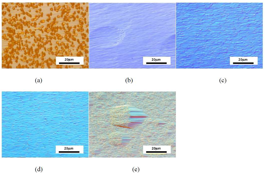
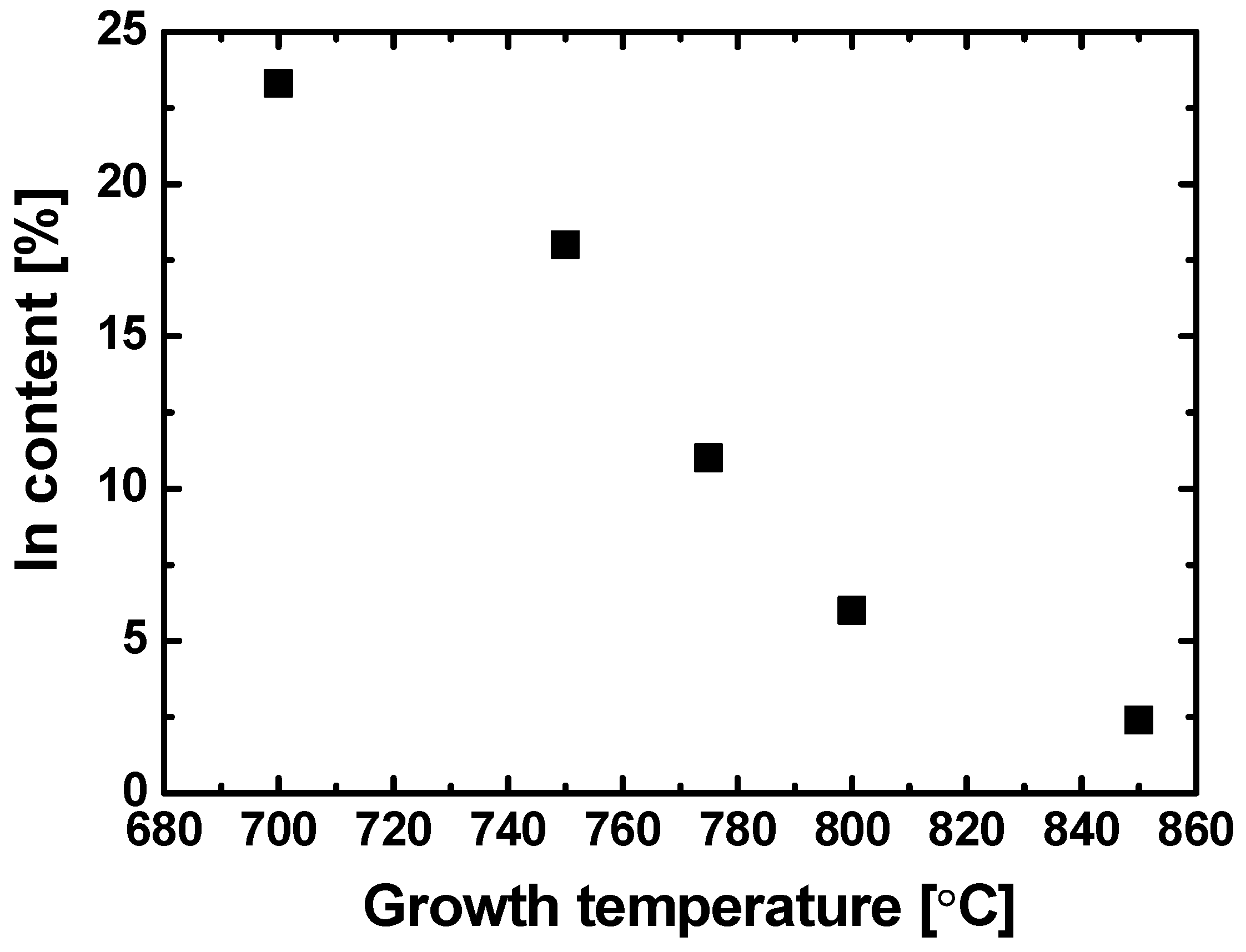
3.1. Characterization of the {11-22} InGaN Layer

First, we characterized the InGaN layers grown on the {11-22} GaN templates, which were obtained at growth temperatures from 700 to 850 °C, with different In contents. Figure 1 shows the images of the epilayer surfaces obtained by differential interference contrast microscopy (Nomarski microscopy). When the growth temperature was 700 °C, many large hillocks were generated on the smooth surface of the GaN base layer. The migration of Ga atoms is considered to be insufficient below a specific temperature, which in this study was 700 °C, resulting in the formation of hillocks. This can also be attributed to the supersaturation of the In molecule toward nitrogen, induced by the low growth temperature, thereby forming an inversion domain, which was observed in the {11-22} GaN layer [35]. On the other hand, the surface morphology was quite smooth when the growth temperature exceeded 750 °C. We confirmed by XRD and RSM analyses in our previous study that a perfectly relaxed InGaN layer could be formed even at the lowest In content of 2% [36,37]. The relaxation mechanism of the InGaN layers was investigated as follows. First, the on-axis RSM of the 11-22 diffraction was observed. We obtained XRD spectra for both the azimuths of the X-ray beam incident along the [-1-123] and [1-100] directions. The crystal properties of {11-22} InGaN varied in the plane depending on the direction of the incident X-ray because of its anisotropy [38,39,40]. The relaxation of {11-22} InGaN can be attributed to the misfit dislocations along the dislocation line parallel to the m-axis. Therefore, the fully relaxed {11-22} InGaN tilts toward the [-1-123] direction from the GaN layer [41]. This offset indicates a macroscopic tilt in the crystal lattice of the InGaN layer and is observable in RSM when the incident X-ray beam is parallel to the [1-123] axis. This result demonstrates that {11-22} InGaN is relaxed if the Qx values of {11-22} InGaN differ from those of GaN. The RMS results showed that all of the samples grew fully relaxed.
The In content was determined from the XRD results according to Vegard’s law, and the relationship between the In content and growth temperature is shown in Figure 2. The optimization of InGaN growth was not performed. The InGaN layers prepared with the In content of less than 18% exhibited a smooth surface. We have previously analyzed these samples by transmission electron microscopy (TEM). When the In content was low, few misfit dislocations existed at the interface between InGaN and GaN, and they did not form threading dislocations. However, a high density of misfit dislocations was generated in the InGaN layers prepared with high In content. We also carried out the ELO of InGaN with an In content greater than 10%; however, we did not succeed in growing a smooth InGaN layer. Thus, to maintain the quality of the InGaN layers and high migration of Ga, the ELO of InGaN was carried out at In contents of less than 6% in this study.

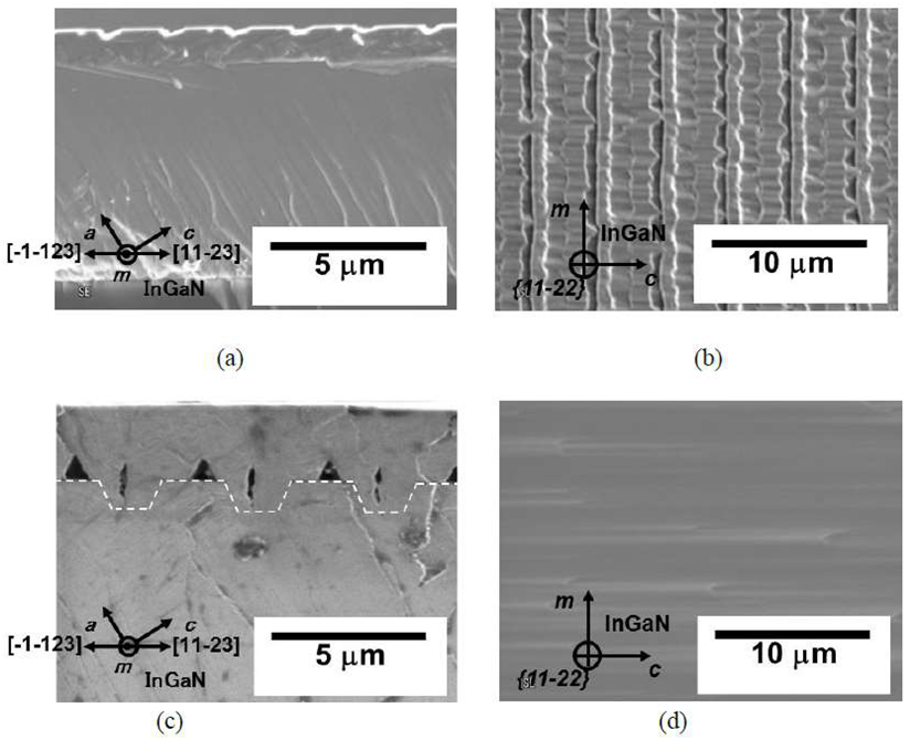
3.2. Epitaxial Lateral Overgrowth of InGaN on the GaN Template

For the ELO of InGaN, a trench-patterned {11-22} GaN template with a SiO2 mask on the terrace was prepared initially, as shown in Figure 3. Striped patterns were formed along the m-axis, parallel to the <11-23> direction, to reduce the formation of SFs by ELO. Here, the InGaN layer is believed to have grown from the sidewall, which is called sidewall ELO. The trench and groove widths were both 2 µm. A growth temperature of 800 °C was used for the ELO of the InGaN layer.
Figure 4 shows the cross-sectional and the plan-view scanning electron microscopy (SEM) images of the InGaN layers at the initial stage of growth and after coalescence. During the initial stages of growth, an undulating surface morphology oriented toward the <11-23> direction was observed. The InGaN growth occurred on both the sidewalls of the GaN template. Furthermore, the InGaN nuclei formed on the SiO2 stripe masks. A smooth surface was not obtained after coalescence because of the above-mentioned anomalous growth on the masks. Two kinds of anomalous morphologies were observed: one was hexagonal and the other was an inclined c-plane crystal, as shown in Figure 4d. The hexagonal morphologies are believed to have originated from the nucleation observed on the SiO2 mask in the initial stages. RSM was performed to elucidate the origin of the inclined c-plane crystal.

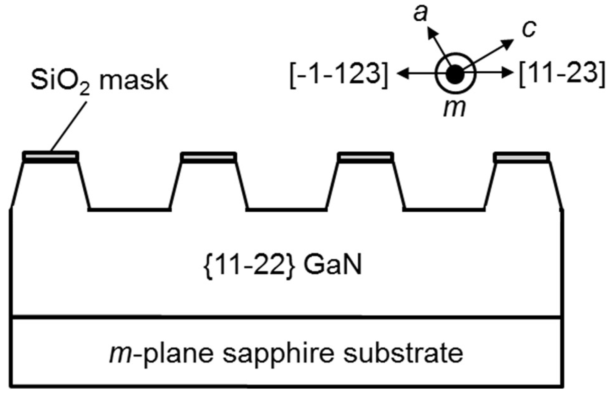
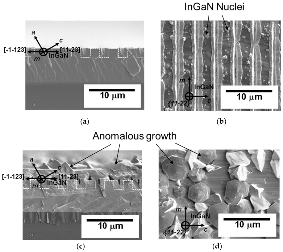
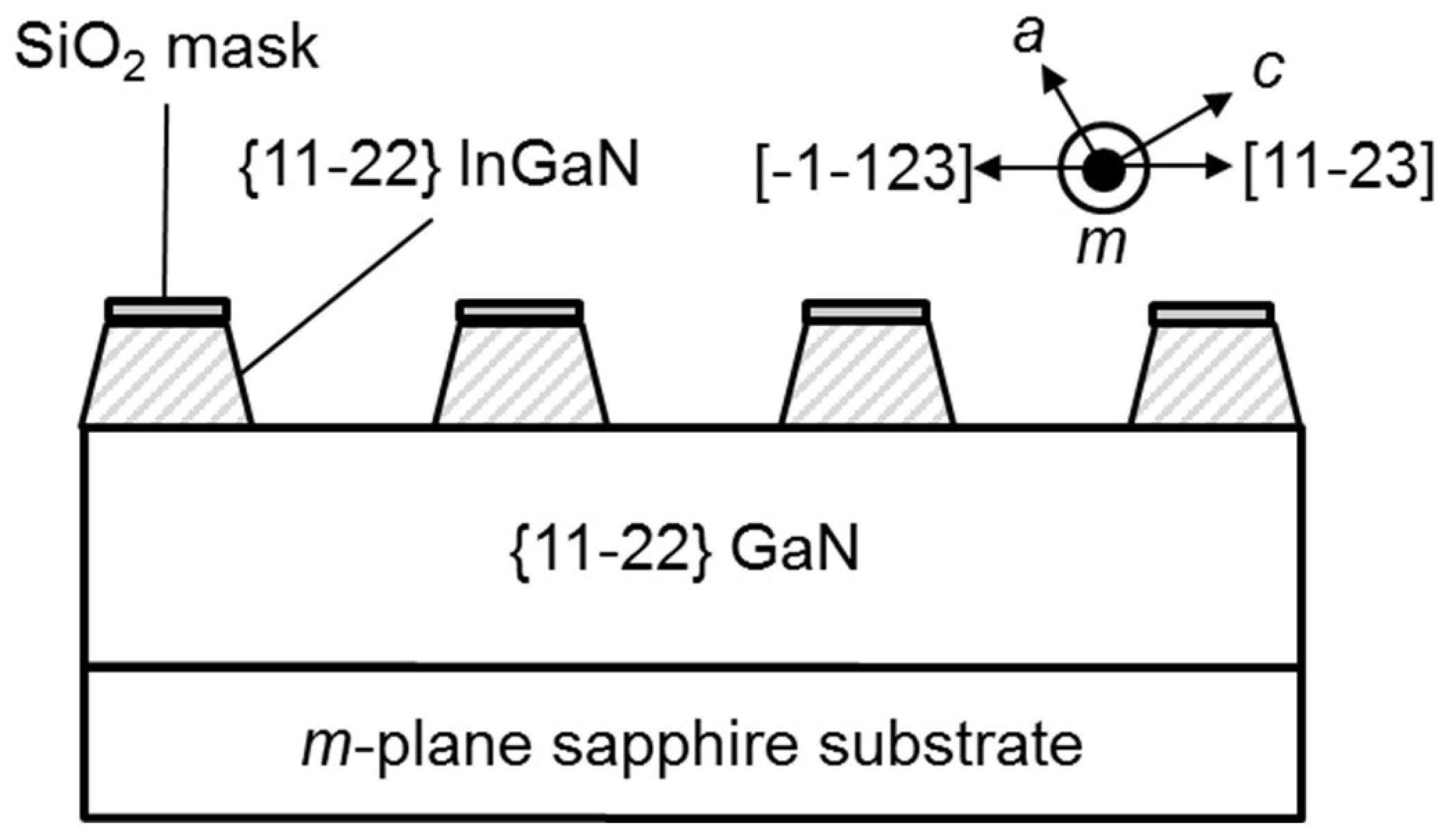
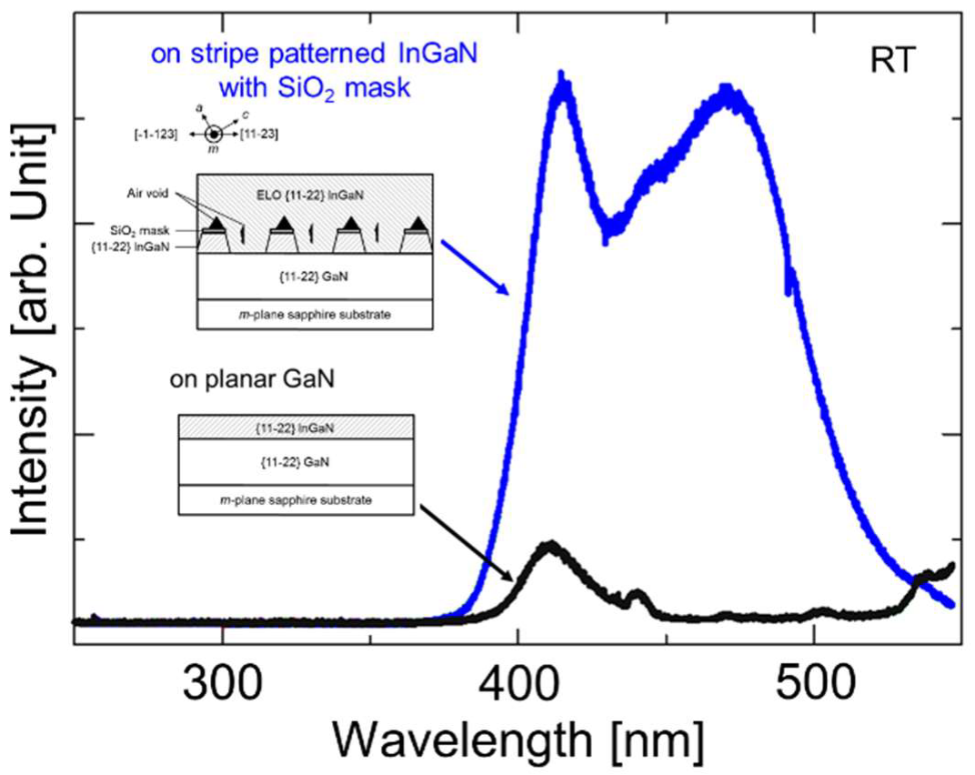
3.3. Epitaxial Lateral Overgrowth of InGaN on an InGaN Template with a SiO2 Mask
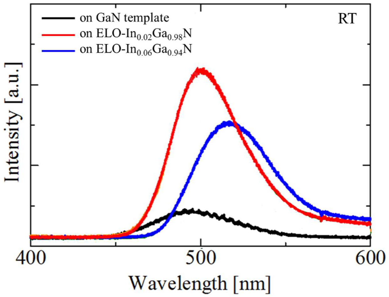
For the ELO of InGaN with better surface morphology, a trench-patterned {11-22} InGaN template with a SiO2 mask on the terraces was prepared, as shown in Figure 5. Similar striped patterns, with trench and groove widths of 2 µm, were formed on the GaN template along the m-axis. The thicknesses of all the base layers were 2 μm, which corresponded to the thickness of the InGaN template, in order to expose the underlying GaN layer. Therefore, the sidewalls were composed of only the InGaN layers. A growth temperature of 800 °C was used for the ELO of the InGaN layer, which was the same as the growth temperature of the base InGaN layer. The growth conditions including the growth time were identical to those of the trench-patterned {11-22} GaN template.
Figure 6 shows the cross-sectional and plan-view SEM images of the InGaN layers at the initial stage of growth and after coalescence. At the initial growth stage, there was no nucleation on the SiO2 mask on the InGaN template. The InGaN growth occurred on both the sidewalls of the InGaN template, in a manner similar to the growth on the patterned GaN template. In the semipolar and nonpolar growths, -c-plane growth promoted the generation of stacking faults. A smooth surface was obtained after coalescence. For the regrown InGaN layer, the film thicknesses were 3.6 μm and 2.5 μm from the trench top and bottom to the surface, respectively. The XRC-FWHMs for the symmetric 11-22 reflection with the azimuth of the X-ray parallel to the <10-10> and <11-23> directions of the sample were 1328 and 796 arcsec, respectively. These values were lower than those of the materials grown on the GaN template (1679 and 1116 arcsec, respectively). Thus, it appears that the crystallinity can be improved by adopting the ELO technique for semipolar {11-22} InGaN layers.
The drastic differences observed in the growth modes of ELO-InGaN on the patterned GaN and InGaN templates were caused by the greater incorporation of In on the patterned InGaN template than on the patterned GaN template due to the compositional pulling effect of In. The higher incorporation of In suppressed the parasitic nucleation on the mask. Thus, a smaller lattice mismatch promoted the ELO of InGaN layers. Our hypothesis regarding the nucleation on the stripe mask is as follows. The partial pressures of Ga and In species in the gas phase over the mask were almost the same at the initial stage of regrowth on InGaN. However, when the In incorporation in the InGaN layer on the InGaN sidewall was greater, the In species on the mask could be reduced because of the different concentration gradient of In in the gas phase. Consequently, the static state of the In species in the gas phase could differ between the GaN and InGaN templates. Alternately, there is a possibility that in the case of regrowth on the patterned GaN template, the nucleation of InGaN on GaN is partially impaired because of the differences in the lattice constants. As a result, the probability of nucleation on the mask is higher than that on the InGaN stripes.
To investigate the crystalline quality of the ELO-InGaN layer based on the optical properties, we recorded the PL spectra. Figure 7 shows the PL spectra at RT of the InGaN layers grown on the planar GaN template and stripe-patterned InGaN template with SiO2 masks. As can be seen in the figure, the PL intensity of ELO-InGaN on the stripe-patterned InGaN template with the SiO2 mask was approximately five times higher than that of the InGaN layer grown on the GaN template. Thus, the effect of ELO on the improvement in the crystalline quality was confirmed. The FWHMs of the PL spectra of the ELO-InGaN layers were greater than those of the InGaN layers on the GaN template, which confirmed the ELO and the change in the In content during ELO. The ELO-InGaN layer was relatively flat, but the In content was 0.5% higher than that of the InGaN template, which can be attributed to the greater incorporation of In during the growth of InGaN toward both the [11-2-3] and [-1-123] directions, similar to the {10-11} plane. The five-times-stronger emission intensity of the ELO-InGaN layer, at approximately 415 nm, was due to the ELO, which improved the crystal quality of the InGaN layer. In addition, a void structure was formed in the layer, which could slightly enhance the light extraction. These account for the higher emission wavelength of the ELO-InGaN template [42,43,44]. The PL spectrum of the ELO-InGaN layer was composed of two peaks at 415 and 470 nm. The peak at 470 nm was considered to be a deep level emission; however, the 470 nm peak was present at a smaller wavelength than the equivalent yellow luminescence observed in GaN. We believe that this emission is not due to (11-22), but could be caused by a plane that appears at ELO, which is neither the c-plane nor (11-22), because it is more prominent at ELO. The mechanism has not yet been fully understood and further investigation should be conducted.

4. Discussion

We succeeded in growing high quality ELO-InGaN layers using a patterned InGaN template. In this section, we compare the optical properties of InGaN/GaN MQWs grown on the GaN and ELO-InGaN templates. Here, the two ELO-InGaN layers were grown at different temperatures while the other parameters were identical. The growth temperatures of these InGaN layers were the same for the base and regrowth layers; for the ELO-InGaN layers with 2% and 6% In composition, the growth temperatures were 850 °C and 800 °C, respectively. Both the trench-patterned InGaN base layers had the same structure as in Figure 6. The thicknesses of both the regrown ELO-InGaN layers were almost the same. In other words, the two InGaN templates were considered to be equivalent in performance except for the In composition. We prepared the ELO-InGaN layers with In contents of 2% and 6%. Figure 8 shows the RT-PL spectra of the InGaN/GaN MQWs grown on the GaN and ELO-InGaN templates. The intensities of the MQWs grown on the ELO-InGaN layers with In contents of 2% and 6% were approximately five and three times stronger than that of the MQWs grown on the GaN layer, respectively. These results indicate that there was a marked improvement in the crystalline quality due to the presence of ELO-InGaN layers. The peak wavelengths of the MQWs on the GaN template and InGaN templates with In contents of 2% and 6% were different due to the In pulling effect. The peak wavelengths of the MQWs grown on the GaN layer and InGaN layers with In contents of 2% and 6% were 493, 501, and 517 nm, respectively. We also calculated the In content of the InGaN well layer based on the peaks present in each PL spectrum. We employed the modified Vegard’s law including the linear interpolation and quadratic term based on a bowing parameter, obtained from previous studies [45]. The In contents of the InGaN well layers in the InGaN/GaN MQWs on the GaN template and InGaN layers with In contents of 2% and 6% were estimated to be 21.9%, 23.0%, and 25.0%, respectively. When the In content in the InGaN template was higher, the lattice mismatch between the MQW and InGaN template was smaller. The higher intensity of the MQWs on the ELO-InGaN layers resulted from the high-quality ELO-InGaN template and suppression of the generation of dislocations and SFs between the InGaN and the MQWs. The emission wavelength increased with an increase in the In content in the InGaN template because of the higher In content due to the efficient In pulling effect in the MQWs.

5. Conclusions

We report the growth of a completely relaxed and thick {11-22}-oriented InGaN layer using the ELO technique. We succeeded in growing an ELO-InGaN layer on a patterned InGaN template. However, it was difficult to fabricate high-quality ELO-InGaN layers on patterned GaN templates. The number of high-density dislocations decreased as the In content decreased. The XRD analysis indicated that the ELO of the InGaN layer should be carried out on relaxed InGaN templates. The FWHM of the 11-22 reflection parallel to <10-10> of ELO-InGaN in the XRC was smaller compared to that of the non-ELO InGaN grown on the {11-22} GaN template. The intensities of the MQWs grown on the ELO-InGaN layers with In contents of 2% and 6% were approximately five and three times higher than that on the GaN layer, respectively. Future research will involve evaluating the SFs of the ELO-InGaN layers and TEM analyses of the dislocation behavior within the layers.

Author Contributions

Conceptualization, N.O. and K.T.; writing—original draft preparation, N.O.; writing—review and editing, N.O.; supervision, K.T.; project administration, K.T.; funding acquisition, K.T. All authors have read and agreed to the published version of the manuscript.

Funding

This research was funded by NEDO grant number I-D2.

Conflicts of Interest

The authors declare no conflict of interest.

References

  1. Narukawa, Y.; Ichikawa, M.; Sanga, D.; Sano, M.; Mukai, T. White light emitting diodes with super-high luminous efficacy. J. Phys. D Appl. Phys. 2010, 43, 354002. [Google Scholar] [CrossRef]
  2. Shioda, T.; Yoshida, H.; Tachibana, K.; Sugiyama, N.; Nunoue, S. Enhanced light output power of green LEDs employing AlGaN interlayer in InGaN/GaN MQW structure on sapphire (0001) substrate. Phys. Stat. Solidi A 2012, 209, 473. [Google Scholar] [CrossRef]
  3. Hashimoto, R.; Hwang, J.; Saito, S.; Nunoue, S. High-efficiency green-yellow light-emitting diodes grown on sapphire (0001) substrates. Phys. Stat. Solidi C 2013, 10, 1529. [Google Scholar] [CrossRef]
  4. Krames, M.R.; Shchekin, O.B.; Mach, R.M.; Mueller, G.O.; Zhou, L.; Harbers, G.; Craford, M.G. Status and future of high-power light-emitting diodes for solid-state lighting. J. Display Tech. 2007, 3, 160. [Google Scholar] [CrossRef]
  5. Iida, D.; Niwa, K.; Kamiyama, S.; Ohkawa, K. Demonstration of InGaN-based orange LEDs with hybrid multiple-quantum-wells structure. Appl. Phys. Express 2016, 9, 111003. [Google Scholar] [CrossRef]
  6. Enya, Y.; Yoshizumi, Y.; Kyono, T.; Akita, K.; Ueno, M.; Adachi, M.; Sumitomo, T.; Tokuyama, S.; Ikegami, T.; Katayama, K.; et al. 531 nm green lasing of InGaN based laser diodes on semi-polar {20-21} free-standing GaN substrates. Appl. Phys. Express 2009, 2, 082101. [Google Scholar] [CrossRef]
  7. Takeuchi, T.; Amano, H.; Akasaki, I. Theoretical study of orientation dependence of piezoelectric effects in wurtzite strained GaInN/GaN heterostructures and quantum wells. Jpn. J. Appl. Phys. 2000, 39, 413. [Google Scholar] [CrossRef]
  8. Liu, R.; Mei, J.; Srinivasan, S.; Ponce, F.A.; Omiya, H.; Narukawa, Y.; Mukai, T. Generation of misfit dislocations by basal-plane slip in InGaN/GaN heterostructures. Appl. Phys. Lett. 2006, 89, 201911. [Google Scholar] [CrossRef]
  9. Hirasaki, T.; Asano, K.; Banno, M.; Ishikawa, M.; Sakuma, F.; Murakami, H.; Kumagai, Y.; Koukitu, A. Growth of thick InGaN layers by tri-halide vapor phase epitaxy. Jpn. J. Appl. Phys. 2014, 53, 05FL02. [Google Scholar] [CrossRef]
  10. Tsai, W.-C.; Hsu, C.-H.; Fu, S.-F.; Lee, F.-W.; Chen, C.-Y.; Chou, W.-C.; Chen, W.-K.; Chang, W.-H. Optical properties associated with strain relaxations in thick InGaN epitaxial films. Opt. Express 2014, 22, A416. [Google Scholar] [CrossRef] [Green Version]
  11. Yamamoto, A.; Hasan, T.M.; Kodama, K.; Shigekawa, N.; Kuzuhara, M. Growth temperature dependent critical thickness for phase separation in thick (~1 μm) InxGa1−xN (x = 0.2–0.4). J. Cryst. Growth 2015, 419, 64. [Google Scholar] [CrossRef]
  12. Papadomanolaki, E.; Bazioti, C.; Kazazis, S.A.; Androulidaki, M.; Dimitrakopulos, G.P. Molecular beam epitaxy of thick InGaN (0001) films: Effects of substrate temperature on structural and electronic properties. J. Cryst. Growth 2016, 437, 20. [Google Scholar] [CrossRef]
  13. Hestroffer, K.; Wu, F.; Li, H.; Lund, C.; Keller, S.; Speck, J.S.; Mishra, U.K. Relaxed c-plane InGaN layers for the growth of strain-reduced InGaN quantum wells. Semicond. Sci. Technol. 2015, 30, 105015. [Google Scholar] [CrossRef]
  14. Sharma, T.K.; Towe, E. A method for evaluating the ground state excitonic band gaps of strained InxGa1−xN/GaN quantum wells. J. Appl. Phys. 2009, 106, 104509. [Google Scholar] [CrossRef]
  15. Okada, N.; Yamada, Y.; Tadatomo, K. Structural and optical evaluation of InGaN/GaN multi-quantum wells on template consisting of in-plane alternately arranged relaxed InGaN and GaN. J. Appl. Phys. 2012, 111, 043508. [Google Scholar] [CrossRef]
  16. Däuebler, J.; Passow, T.; Aidam, R.; Köhler, K.; Kirste, L.; Kunzer, M.; Wagner, J. Long wavelength emitting GaInN quantum wells on metamorphic GaInN buffer layers with enlarged in-plane lattice parameter. Appl. Phys. Lett. 2014, 105, 111111. [Google Scholar] [CrossRef]
  17. Hiramatsu, K.; Nishiyama, K.; Motogaito, A.; Miyake, H.; Iyechika, Y.; Maeda, T. Recent progress in selective area growth and epitaxial lateral overgrowth of III-nitrides: Effects of reactor pressure in MOVPE growth. Phys. Status Solidi A 1999, 176, 535. [Google Scholar] [CrossRef]
  18. Tyagi, A.; Wu, F.; Young, E.C.; Chakraborty, A.; Ohta, H.; Bhat, R.; Fujito, K.; DenBaars, S.P.; Nakamura, S.; Speck, J.S. Partial strain relaxation via misfit dislocation generation at heterointerfaces in (Al, In)GaN epitaxial layers grown on semipolar GaN free standing substrates. Appl. Phys. Lett. 2009, 95, 251905. [Google Scholar] [CrossRef]
  19. Wu, Z.H.; Tanikawa, T.; Murase, T.; Fang, Y.-Y.; Chen, C.Q.; Honda, Y.; Yamaguchi, M.; Amano, H.; Sawaki, N. Partial strain relaxation by stacking fault generation in InGaN multiple quantum wells grown on (1-101) semipolar GaN. Appl. Phys. Lett. 2011, 98, 051902. [Google Scholar] [CrossRef]
  20. Kuwahara, T.; Kuwano, N.; Kurisu, A.; Okada, N.; Tadatomo, K. Behavior of misfit dislocations in semipolar InGaN/GaN grown by MOVPE. Phys. Stat. Solidi. C 2012, 9, 488. [Google Scholar] [CrossRef]
  21. Senda, R.; Miura, A.; Hayakawa, T.; Kawashima, T.; Iida, D.; Nagai, T.; Iwaya, M.; Kamiyama, S.; Amano, H.; Akasaki, I. Realization of high-crystalline-quality thick m-plane GaInN film on 6H-SiC substrate by epitaxial lateral overgrowth. Jpn. J. Appl. Phys. 2007, 46, L948. [Google Scholar] [CrossRef]
  22. Senda, R.; Miura, A.; Kawashima, T.; Iida, D.; Nagai, T.; Iwaya, M.; Kamiyama, S.; Amano, H.; Akasaki, I.; Akasaki, I. Improvement in crystalline quality of thick GaInN on m-plane 6H-SiC substrates using sidewall epitaxial lateral overgrowth. Phys. Stat. Solidi C 2008, 5, 3045. [Google Scholar] [CrossRef]
  23. Ozaki, T.; Takagi, Y.; Nishinaka, J.; Funato, M.; Kawakami, Y. Metalorganic vapor phase epitaxy of GaN and lattice-matched InGaN on ScAlMgO4 (0001) substrates. Appl. Phys. Express 2014, 7, 091001. [Google Scholar] [CrossRef]
  24. Okada, N.; Inomata, Y.; Ikeuchi, H.; Fujimoto, S.; Itakura, H.; Nakashima, S.; Kawamura, R.; Tadatomo, K. Characterization of high-quality relaxed flat InGaN template fabricated by combination of epitaxial lateral overgrowth and chemical mechanical polishing. J. Cryst. Growth 2019, 512, 147. [Google Scholar] [CrossRef]
  25. White, R.C.; Khoury, M.; Wu, F.; Keller, S.; Rozhavskaia, M.; Sotta, D.; Nakamura, S.; DenBaars, S.P. MOCVD growth of thick V-pit-free InGaN films on semi-relaxed InGaN substrates. Semicond. Sci. Technol. 2021, 36, 015011. [Google Scholar] [CrossRef]
  26. White, R.C.; Khoury, M.; Wong, M.S.; Li, H.; Lynsky, C.; Iza, M.; Keller, S.; Sotta, D.; Nakamura, S.; DenBaars, S.P. Realization of III-nitride c-plane microleds emitting from 470 to 645 nm on semi-relaxed substrates enabled by v-defect-free base layers. Crystals 2021, 11, 1168. [Google Scholar] [CrossRef]
  27. Wong, M.S.; Chan, P.; Lim, N.; Zhang, H.; White, R.C.; Speck, J.S.; Denbaars, S.P.; Nakamura, S. Low forward voltage III-nitride red micro-light-emitting diodes on a strain relaxed template with an InGaN decomposition layer. Crystals 2022, 12, 721. [Google Scholar] [CrossRef]
  28. White, R.C.; Li, H.; Khoury, M.; Lynsky, C.; Iza, M.; Keller, S.; Sotta, D.; Nakamura, S.; DenBaars, S.P. InGaN-based microLED devices approaching 1% EQE with red 609 nm electroluminescence on semi-relaxed substrates. Crystals 2021, 11, 1364. [Google Scholar] [CrossRef]
  29. Horng, R.H.; Ye, C.-X.; Chen, P.-W.; Iida, D.; Ohkawa, K.; Wu, Y.-R.; Wuu, D.-S. Study on the effect of size on InGaN red micro-LEDs. Sci. Rep. 2022, 12, 1324. [Google Scholar] [CrossRef]
  30. Li, P.; Li, H.; Wong, M.S.; Chan, P.; Yang, Y.; Zhang, H.; Iza, M.; Speck, J.S.; Nakamura, S.; Denbaars, S.P. Progress of InGaN-based red micro-light emitting diodes. Crystals 2022, 12, 541. [Google Scholar] [CrossRef]
  31. Wakahara, A.; Sekiguchi, H.; Okada, H.; Takagi, Y. Current status for light-emitting diode with Eu-doped GaN active layer grown by MBE. J. Lumin. 2012, 132, 3113. [Google Scholar] [CrossRef]
  32. Li, P.; Li, H.; Zhang, H.; Lynsky, C.; Iza, M.; Speck, J.S.; Nakamura, S.; DenBaars, S.P. Size-independent peak external quantum efficiency (>2%) of InGaN red micro-light-emitting diodes with an emission wavelength over 600 nm. Appl. Phys. Lett. 2021, 119, 081102. [Google Scholar] [CrossRef]
  33. Zhao, G.; Wang, L.; Yang, S.; Li, H.; Wei, H.; Han, D.; Wang, Z. Anisotropic structural and optical properties of semi-polar (11–22) GaN grown on m-plane sapphire using double AlN buffer layers. Sci. Rep. 2016, 6, 20787. [Google Scholar] [CrossRef] [PubMed]
  34. Lotsari, A.; Das, A.; Kehagias, T.; Kotsar, Y.; Monroy, E.; Karakostas, T.; Gladkov, P.; Komninou, P.; Dimitrakopulos, G.P. Morphology and origin of V-defects in semipolar (11–22) InGaN. J. Cryst. Growth 2021, 339, 1. [Google Scholar] [CrossRef]
  35. Okada, N.; Okamura, Y.; Uchida, K.; Tadatomo, K. Controlling optical polarization of {11–22} semipolar multiple quantum wells using relaxed underlying InGaN buffer layers. Opt. Mater. 2016, 58, 243. [Google Scholar] [CrossRef]
  36. Tawarazako, Y.; Nishi, N.; Nakata, A.; Okada, N.; Kurai, S.; Yamada, Y.; Tadatomo, K. Long wavelength red to green emissions from {11-22} semipolar multi-quantum wells on fully relaxed InGaN underlayer. Jpn. J. Appl. Phys. 2021; under review. [Google Scholar]
  37. Lee, S.-N.; Klm, K.K.; Nam, O.H.; Klm, J.H.; Klm, H. Structural and optical characterization of (11–22) semipolar GaN on m-plane sapphire without low temperature buffer layer. Phys. Stat. Solidi C 2010, 7, 2043. [Google Scholar] [CrossRef]
  38. Wernicke, T.; Netzel, C.; Weyers, M.; Kneissl, M. Semipolar GaN grown on m-plane sapphire using MOVPE. Phys. Stat. Solidi 2008, 5, 1815. [Google Scholar] [CrossRef]
  39. Kappers, M.J.; Hollander, J.L.; McAleese, C.; Johnston, C.F.; Broom, R.F.; Barnard, J.S.; Vickers, M.E.; Humphreys, C.J. Growth and characterisation of semi-polar ( 11 2 - 2 ) InGaN/GaN MQW structures. J. Cryst. Growth 2007, 300, 155. [Google Scholar] [CrossRef]
  40. Romanov, A.E.; Young, E.C.; Wu, F.; Tyagi, A.; Gallinat, C.S.; Nakamura, S.; DenBaars, S.P.; Speck, J.S. Basal plane misfit dislocations and stress relaxation in III-nitride semipolar heteroepitaxy. J. Appl. Phys. 2011, 109, 103522. [Google Scholar] [CrossRef]
  41. Keller, S.; Fichtenbaum, N.A.; Furukawa, M.; Speck, J.S.; DenBaars, S.P.; Mishra, U.K. Growth and characterization of N-polar InGaN/GaN multiquantum wells. Appl. Phys. Lett. 2007, 90, 191908. [Google Scholar] [CrossRef]
  42. Wernicke, T.; Schade, L.; Netzel, C.; Rass, J.; Hoffmann, V.; Ploch, S.; Knauer, A.; Weyers, M.; Schwarz, U.; Kneissl, M. Indium incorporation and emission wavelength of polar, nonpolar and semipolar InGaN quantum wells. Semicond. Sci. Technol. 2012, 27, 024014. [Google Scholar] [CrossRef]
  43. Wunder, T.; Feneberg, M.; Lipski, F.; Wang, J.; Leute, R.A.; Schwaiger, S.; Thonke, K.; Chuvilin, A.; Schwarz, U.T.; Dräger, A.D.; et al. Three-dimensional GaN for semipolar light emitters. Phys. Stat. Solidi B 2011, 248, 549. [Google Scholar] [CrossRef]
  44. Orsal, G.; Gmili, Y.E.; Fressengeas, N.; Streque, J.; Djerboub, R.; Moudakir, T.; Sundaram, S.; Ougazzaden, A.; Salvestrini, J.P. Bandgap energy bowing parameter of strained and relaxed InGaN layers. Opt. Mater. Express 2014, 4, 1030. [Google Scholar] [CrossRef]
  45. Kurouchi, M.; Araki, T.; Naoi, H.; Yamaguchi, T.; Suzuki, A.; Nanishi, Y. Growth and properties of In-rich InGaN films grown on (0001) sapphire by RF-MBE. Phys. Stat. Solidi B 2004, 241, 2843. [Google Scholar] [CrossRef]
Figure 1. Nomarski images of InGaN layers with different In contents grown on the {11-22} GaN templates at (a) 700, (b) 750, (c) 775, (d) 800, and (e) 850 °C.
Crystals 12 01373 g001
Figure 2. The relationship between the In content and growth temperature.
Crystals 12 01373 g002
Figure 3. A schematic illustration of the trench-patterned {11-22} GaN template with a SiO2 mask on the terraces.
Crystals 12 01373 g003
Figure 4. Cross-sectional and plan-view SEM images of the {11-22} InGaN layers grown on the GaN template at a growth temperature of 800 °C, at the initial stage of growth (a,b), and after coalescence (c,d).
Crystals 12 01373 g004
Figure 5. A schematic illustration of the trench-patterned {11-22} InGaN template with a SiO2 mask on the terraces.
Crystals 12 01373 g005
Figure 6. Cross-sectional and plan-view SEM images of the {11-22} InGaN layers grown on the InGaN template at a growth temperature of 800 °C, at the initial stage of growth (a,b), and after coalescence (c,d).
Crystals 12 01373 g006
Figure 7. The PL spectra of the {11-22} InGaN layers grown on the planar GaN template and stripe-patterned InGaN template with SiO2 masks.
Crystals 12 01373 g007
Figure 8. The PL spectra of the {11-22} InGaN/GaN MQWs on the GaN and ELO-InGaN templates.
Crystals 12 01373 g008
Publisher’s Note: MDPI stays neutral with regard to jurisdictional claims in published maps and institutional affiliations.

