Article

Optical Properties of InGaN/GaN QW with the Same Well-Plus-Barrier Thickness

Laboratory of Micro/Nano-Optoelectronics, Department of Microelectronics and Integrated Circuits, Xiamen University, Xiamen 361005, China
*
Authors to whom correspondence should be addressed.
Crystals 2022, 12(1), 114; https://doi.org/10.3390/cryst12010114
Submission received: 12 December 2021 / Revised: 13 January 2022 / Accepted: 14 January 2022 / Published: 15 January 2022
(This article belongs to the Special Issue Advances in GaN-Based Optoelectronic Materials and Devices)

Abstract

:
Optical properties of wurtzite violet InGaN/GaN quantum well (QW) structures, with the same well-plus-barrier thickness, grown by metal-organic chemical vapor deposition (MOCVD) on c-plane sapphire substrates, were investigated using temperature-dependent photoluminescence (TDPL) and excitation-power-dependent photoluminescence (PDPL). Two samples were compared: one had a thicker well (InGaN/GaN 3/5 nm); the other had a thicker barrier (InGaN/GaN 2/6 nm). It was found that the GaN barrier thickness in the InGaN/GaN MQWs plays an important role in determining the optical characteristics of the MQWs. The peak energy of the two samples varied with temperature in an S-shape. The thicker-barrier sample had a higher turning point from blueshift to redshift, indicating a stronger localization effect. From the Arrhenius plot of the normalized integrated PL intensity, it was found that the activation energy of the nonradiative process also increased with a thicker barrier thickness. The radiation recombination process was dominated in the sample of the thicker barrier, while the non-radiation process cannot be negligible in the sample of the thicker well.

1. Introduction

During the past decades, group III nitride materials have attracted great attention. InGaN/GaN multiple quantum well (MQW) structures are currently utilized as the active layers for most optoelectronic devices due to their excellent performance, such as ultraviolet-visible tunable emission band [1], thermal stability, and high quantum efficiency [2]. The energy bandgap tunability of InGaN makes it possible to manufacture red-, green-, and blue (RGB)-light-emitting diodes (LEDs) using the same material system, which can help to develop the monolithic integration technology for high-performance micro-LED displays. The optical properties of the MQW active regions are influenced by the material quality and structures of InGaN well layers, such as the thickness [3], shape [4], and well number [5]. GaN quantum barriers (QBs) also affect the optical properties of the active layer. This is because that QBs have a higher optimum growth temperature than that of InGaN well layers. Thermal degradation and decomposing in InGaN QWs are promoted by the elevated temperature, which degrades the optical quality of the well layer [6]. Moreover, the barrier thickness can affect the piezoelectric field and the distribution of injected carriers [7] and exciton localization in the well [8]. Therefore, analyzing how well and how barriers affect the optical properties is of great significance for both theoretical researches and practical applications.
At present, a lot of work has been completed on the effect of InGaN well thickness or barrier thickness on the optical properties of InGaN/GaN MQWs. Li et al. [9] proved that a thinner well results in higher internal quantum efficiency (IQE) due to the greater overlap of electron and hole wave functions in space. Huang et al. [10] found that larger well thickness can induce a stronger carrier localization effect by investigating the effect of well thickness on the properties of InGaN/GaN active layers. Jia et al. [11] proved that increasing the GaN barrier thickness can improve the IQE of QD/QW hybrid structures. The results of Liang et al. [12] indicated that the localization effect formed by Indium clusters is stronger for a sample with a thicker barrier. However, these studies keep the thickness of the well (barrier) constant and change the thickness of the barrier (well), leading to different well-plus-barrier thicknesses. This can cause undesirable effects that will influence the optical properties of the MQWs and the final conclusion [13]. For instance, the change in total thickness will lead to a different strain accumulation and relaxation [14]; enhancement of the inhomogeneous of carrier distribution among different wells, especially holes; and variation in cavity lengths in the case of resonant-cavity light-emitting diodes and vertical-cavity surface-emitting lasers. Based on the above, the change of optical properties cannot be simply attributed to the change of well or barrier thickness.
In this paper, two samples with the same well-plus-barrier thickness were grown under the same conditions. The well/barrier layer thickness in the MQW was 3 nm/5 nm for Sample 1 and 2 nm/6 nm for Sample 2, respectively. The optical properties of these two samples were studied by the temperature-dependent photoluminescence (TDPL) and excitation-power-dependent photoluminescence (PDPL) measurements. An S-shaped shift (redshift–blueshift–redshift) of luminescence peak energy is well known for InGaN/GaN quantum wells and usually originates from the existence of potential fluctuations and carrier localization–delocalization process [14,15] was observed. The temperature of the turning point from blueshift to redshift of the S-shaped curve and the activation energy of the nonradiative recombination process is increased in Sample 2. In addition, the band-tail model was employed to evaluate the localization effect. The results suggest weaker localization effects in Sample 1, indicating that the barrier thickness (longer growth time) may play a more important role than the well thickness.

2. Materials and Methods

InGaN/GaN MQW heterostructures Sample 1 and Sample 2 were grown on c-plane sapphire substrates via a low-pressure metalorganic chemical vapor deposition (MOCVD) cold wall system. Ammonia (NH3), trimethylgallium (TMGa), trimethylindium (TMIn), biscyclopentadienylMagnesium (Cp2Mg), and silane (SiH4) were used as the precursors and dopants, and hydrogen and nitrogen as carrier gas. Figure 1 shows the structure of these two samples. The epitaxial structure for both samples includes a 2 μm undoped GaN layer, a 2 μm thick n-type GaN layer, five periods of In0.1Ga0.9N/GaN MQWs, a 20 nm thick Al0.2Ga0.8N electron blocking layer, and a 97-nm thick p-type GaN layer in turn. For better comparison, the growth conditions and structure were identical for both samples, except the active layer. The growth temperatures were 780 °C for the InGaN wells and 880 °C for GaN barriers, respectively. Five periods of In0.1Ga0.9N (3 nm)/GaN (5 nm) quantum wells (QWs) served as the active region for Sample 1, while five periods of In0.1Ga0.9N (2 nm)/GaN (6 nm) QWs for Sample 2.
A continuous-wave He–Cd laser (325 nm) served as excitation source for the TDPL and PDPL. A closed-cycle He-cryostat system was used to control the temperature ranging from 10 to room temperature(RT). The luminescent signal was dispersed by using a Princeton instruments ACTON Spectrapro-3000i monochromator (Princeton Instruments, New Jersey, America) and detected with a Synapse CCD detector (HORIBA, Kyoto, Japan), which is cooled by thermoelectric units.

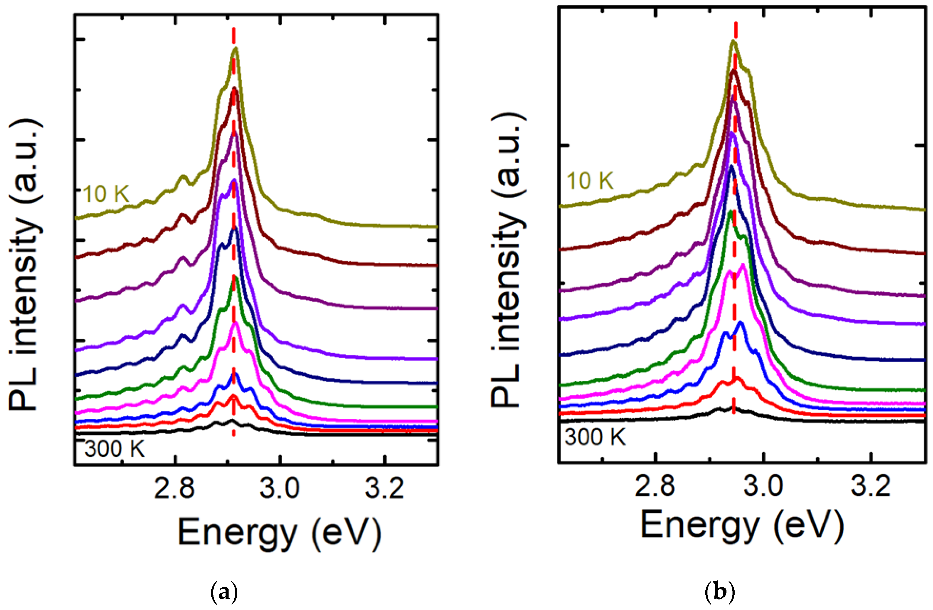
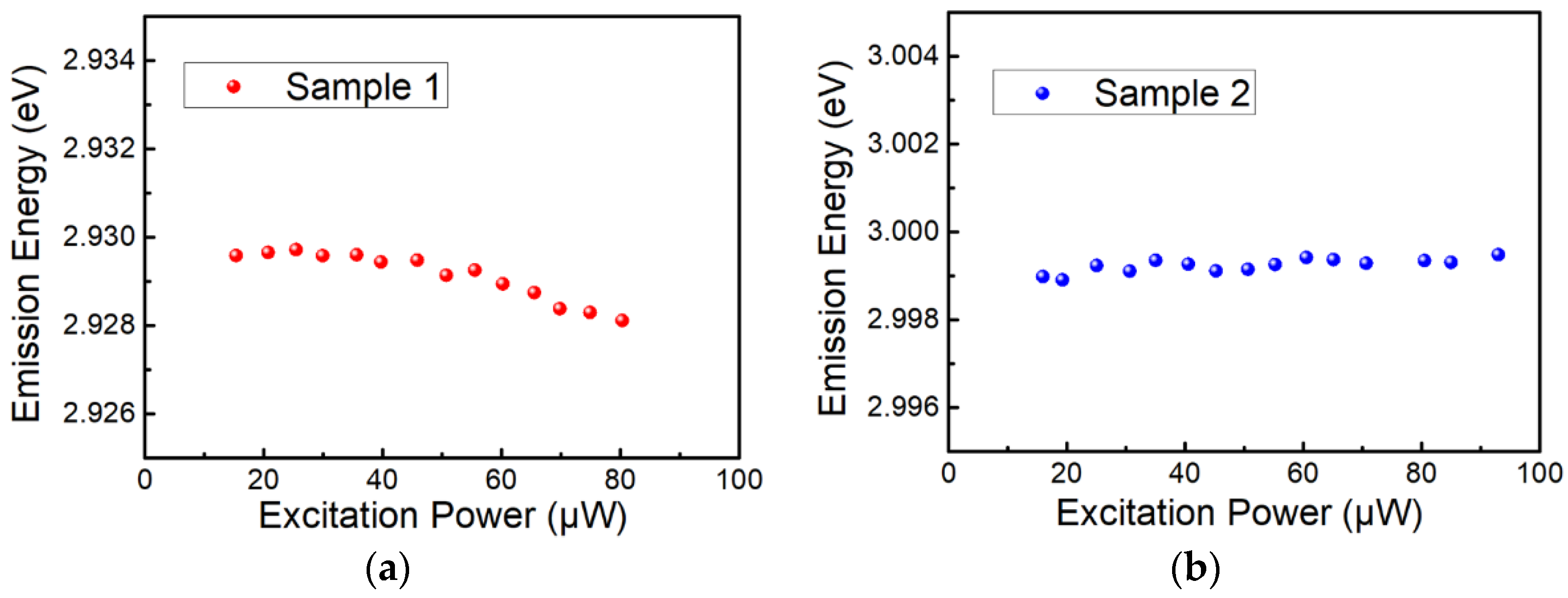
3. Results and Discussion

The PL spectra of (a) Sample 1 and (b) Sample 2 recorded at different temperatures at an 0.02-mW excitation power using the 325 nm He–Cd laser are shown in Figure 2a,b, respectively. These spectra with different temperatures were shifted in the vertical axis to compare their shapes and peak positions. In order to eliminate the influence of Fabry–Perot interference fringe and acquire the accurate peak energy and half-peak full width (FWHM), the Gaussian functions were used to fit all the PL spectra. The peak energy was determined to be 2.901 eV for Sample 1 and 2.935 eV for Sample 2 at room temperature. The bandgap for the InxGa1-xN ternary system without an electric field can be calculated by the following formula [11]:
E g ( I n x G a 1 x N ) = 3.42 2.65 · x 2.4 · x · ( 1 x )   ( e V )  
When the Indium composition is about 10%, the bandgap is calculated to be 2.939 eV. This is very close to the emission energy of the two samples in this study. So the Indium composition is around 10%. Since there are nearly identical growth conditions for the two samples, the Indium content is considered to be similar for Sample 1 and Sample 2 [12]. Considering that the emission energy is decreased with an increasing well thickness owing to the quantum-confinement effect [13], this result is in accordance with the experimental data. That is, Sample 2 exhibits a higher carrier transition energy because of its thinner well thickness. In addition, the electric field in QWs leads to a strong quantum-confined Stark effect (QCSE), which can result in bandgap shrinkage. However, the QCSE in Sample 1 and Sample 2 is negligible, which is supported by the PDPL measurement and will be discussed later. Fluctuation of Indium composition in the active layer is beneficial to localize carriers and hinders their migration toward nonradiative recombination centers. There are several mechanisms that can explain the formation, such as the surface-segregation effect [14], spinodal decomposition [15], and composition-pulling effect [16]. Yen-Sheng Lin et al. [15] showed that it is a spinodal decomposition mechanism rather than a composition pulling effect that dominated the formation of the compositional fluctuations in InGaN/GaN multiple quantum wells with indium content in the range of 15–25%. Given that the composition-pulling effect is strengthened with the increase of Indium composition in the InGaN film, the composition-pulling effect is weak for the 10% low-Indium InGaN layer studied here.
Figure 3 shows the temperature dependence of peak energy and FWHM for the two samples. As the signature of the exciton localization [17], an S-shaped (red–blue–red) shift of luminescence peak energy and a V-shaped (declining-then-rising) FWHM were observed. This phenomenon is well known for InGaN/GaN quantum wells and usually originates from the presence of potential fluctuations and the carrier-transition process between localization and delocalization [18,19]. We named the transition temperature of red–blueshift as Tmin. The valve of Tmin is related to the transition of carriers between shallow and deep localized states. The higher Tmin in Sample 2 implies a severe indium composition fluctuation, which is consistent with the broader FWHM of Sample 2 [20]. The decline in FWHM is mainly related to the migration process of thermally activated carriers from shallow to deep localized states. Additionally, the deep localized states have a higher density of carrier states, resulting in a narrower linewidth and redshifts. The difference between the peak energy and FWHM reveals that the concentration of deep localized centers is lower in Sample 1. The reason for this will be further discussed in a later section. We named the transition temperature of blue–redshift as Tmax, which is related to the depth of localization potential [21]. The values of Tmax are 180 K and 200 K for Sample 1 and Sample 2, respectively. This means that Sample 2 has the comparatively stronger confinement energy than those of localization states in Sample 1 on average. Larger thermal energy is needed for carriers to exit the localization potential.
In order to further investigate the temperature dependence of the PL peak energy, the band-tail model is employed. The model considers the energy levels lower than the nominal band edge, which provides the localized carriers confinement effect [22]. In the band-tail model, the peak energy at various temperatures can be expressed in the following equation [23,24].
E ( T ) = E ( 0 ) α T 2 β + T σ 2 k B T
where E(0), T, and kB is the band-gap energy at 0 K, temperature, and the Boltzmann constant, respectively. α , β are Varshni’s fitting parameters. The parameters σ reflects the degree of localization effect [25]. The model presented in Equation (2) is in good agreement with the experimental data. The fitting parameters α (0.75 meV/K) and β (1300 K) are similar to those used in the literature [26]. The values of σ were fitted to be 18.41 meV and 23.01 meV for Sample 1 and Sample 2, respectively. It is well known that the excellent performance of InGaN-based LEDs is widely ascribed to the carrier localization effect [27]. It is the indium-rich regions in the InGaN well layer with deeper potential levels that serve as localized centers, limiting the outflow of carriers to the surrounding nonradiative recombination centers(NRCs) [28], thus improving the emission efficiency of the quantum well structure. The smaller value of σ indicates weaker localization effects and poor optical performance in Sample 1, which has a thicker well thickness.
However, the decrease in σ with larger well thickness seems to be in conflict with previous publications [10,25,29]. The previous literature pointed out that InGaN/GaN MQW LEDs with thicker well structures have stronger exciton localization effects. The discrepancy between our experimental results and those of the previous reports is that our samples have different barrier thicknesses at the same time, while their samples kept the barrier layer thickness constant. Sample 1 has a thicker well thickness, while Sample 2 has a thicker barrier thickness. Such stronger localization effects in Sample 2 can be attributed to the larger potential fluctuations promoted by larger barrier thickness. The barrier is also essential to the crystal quality and structural properties of InGaN well layers. The thicker barrier needs a longer growth time. Because the optimum growth temperature of GaN barriers is much higher than that of InGaN layers [30], InGaN is thermally annealed during the growth of the barrier, leading to indium desorption and indium segregation [30]. In the case of a thicker barrier where a longer growth time is necessary, this phenomenon will be enhanced, resulting in stronger composition fluctuation and then stronger localization effects in the MQWs.
Figure 4 shows the Arrhenius plots of the integral PL intensity for Sample 1 and Sample 2. The results show that the PL intensities decrease significantly with the increasing temperature, which is attributed to defect-related nonradiative recombination [31,32]. However, a strong localization effect can hinder carriers from diffusion towards NRCs [33]. To further verify the carrier localization effects in two samples, the dependence of the integrated PL intensity on different temperatures was fitted by the following one-channel Arrhenius model [34]:
I ( T ) = 1 1 + N · e x p ( E a / K T )
where parameters N and Ea represent the quantity and activation energy of the nonradiative process, respectively. kB is the Boltzmann constant and T represents temperature. Ea is related to the nonradiative channels introduced by the dislocations [35]. The solid lines in Figure 4 are the best fitting of experimental data of Samples 1 and 2 by Equation (3), and the fitted values are shown in Figure 4. The Ea value for Sample 2 is larger than that for Sample 1, suggesting that the former is less sensitive to NRC. This is consistent with our Varshini fitting results. The strong carrier localization effect in Sample 2 suppresses the possibility of carriers being captured by the NRCs due to the deep localized potential restricting carrier movability, while the photogenerated carriers in Sample 1 will be more easily affected by the defect-related nonradiative centers because of the relatively weaker localization effect.
The explanation is also supported by PDPL. Figure 5 shows the integrated PL intensities (I) for (a) Sample 1 and (b) Sample 2 as functions of excitation power (E). It is known that the relationship between I and E is expressed as I Ep, where parameter P describes the rate between radiative and nonradiative recombination in the QWs [36]. The PL intensity of Sample 2 increases linearly throughout the excitation range. The slope of ~1.03 was obtained by linear fitting, indicating that the radiation recombination process is dominant, while the slope is ~1.39 for Sample 1, suggesting a larger inclusion of the nonradiation process. The longer growth time of the barriers for Sample 2 leads to indium segregation, causing the Indium compositional fluctuation or localized states. These localized states, working as quantum dots, can limit the movement of carriers and make them avoid nonradiative recombination centers caused by dislocations. The strong carrier localization effect in Sample 2 can effectively reduce the possibility of carrier migration into NRCs and thus increase the chance of radiation recombination, which is consistent with the conclusion discussed above.
In addition, the quantum-confined Stark effect (QCSE) in InGaN QWs, which causes a decreasing overlap between electron and hole wave functions and lowers radiative recombination, is investigated. Figure 6 shows the emission energy as a function of excitation power for Sample 1 and Sample 2, respectively. Sample 1 shows a slight redshift (1.47 meV) of emission energy with increasing the excitation power, while the emission energy of Sample 2 is almost independent of the excitation power. It is known that the piezoelectric fields which determine the QCSE in the strained InGaN well layer will be screened by photon-generated carriers, and the transition energy will increase (blueshift). This phenomenon, however, was not observed in our study. These results indicate that the QCSE (or the piezoelectric internal field) in Sample 1 and Sample 2 is negligible. In addition, different from the case of InGaN quantum wells, the QCSE, which causes a decreasing overlap between electron and hole wave functions and lowers the radiative recombination, is expected to be significantly weakened in the localized states. The Indium compositional fluctuation in Sample 2 is considered to be responsible for the better optical properties.

4. Conclusions

In general, the optical properties of the violet-light-emitting InGaN/GaN MQWs with different active region structures were investigated by TDPL and PDPL measurements. The two samples had the same thickness of well-plus-barrier, but one had a thicker well thickness, and the other had a thicker barrier thickness. It was found that the carrier-localization effect was enhanced for the sample with the thicker barrier thickness. By comparing the activation energy of the nonradiative process and the ratio between radiative and nonradiative recombination of the PL peak, the MQW with a thicker barrier thickness was demonstrated to exhibit better optical performance. This is because a thicker barrier means a longer growth time at an elevated temperature, inducing the aggregating of Indium-rich microstructures in the InGaN layers, which improves the sample quality. In conclusion, given the fact that the thicknesses of the barrier and well both strongly affect the optical properties of InGaN/GaN MQWs structures, a moderate barrier and well width are quite necessary.

Author Contributions

Conceptualization, H.X. and X.H.; methodology, H.X. and X.H.; formal analysis, H.X.; investigation, H.X. and L.C.; resources, Y.M. and B.Z.; data curation, H.X. and L.C.; writing—original draft preparation, H.X.; writing—review and editing, X.H., Y.M., and B.Z.; visualization, H.X.; supervision, B.Z.; project administration, Y.M. and B.Z. All authors have read and agreed to the published version of the manuscript.

Funding

This research was funded by the National Key Research and Development Program of China, grant number 2017YFE0131500, the National Natural Science Foundation of China, grant number U21A20493 and 62104204 and President’s Foundation of Xiamen University, grant number ZK1029.

Institutional Review Board Statement

Not applicable.

Informed Consent Statement

Not applicable.

Data Availability Statement

Data underlying the results presented in this paper are not publicly available at this time but may be obtained from the authors upon reasonable request.

Acknowledgments

The authors would like to gratefully acknowledge the support from the National Key Research, Development Program of China and the National Natural Science Foundation of China and President’s Foundation of Xiamen University. The authors thank the reviewers for their constructive comments, which helped the cause of the manuscript.

Conflicts of Interest

The authors declare no conflict of interest.

References

  1. Hou, X.; Fan, S.; Iida, D.; Mei, Y.; Zhang, B.; Ohkawa, K. Photoluminescence of InGaN-based red multiple quantum wells. Opt. Express 2021, 29, 30237–30243. [Google Scholar] [CrossRef]
  2. Liu, W.; Zhao, D.G.; Jiang, D.S.; Chen, P.; Liu, Z.S.; Zhu, J.J.; Li, X.; Shi, M.; Zhao, D.M.; Liu, J.P. Effect of localization states on the electroluminescence spectral width of blue–green light emitting InGaN/GaN multiple quantum wells. J. Vac. Sci. Technol. A Vac. Surf. Film. 2015, 33, 061502. [Google Scholar] [CrossRef]
  3. Younghoon, K.; Changsoo, K.; Samkyu, N.; Jaeyoung, L.; Keeyoung, L.; Byungsung, O. Structural and optical properties of InGaN/GaN multi-quantum well structures with different well widths. MRS Online Proc. Libr. Arch. 2002, 722, 193–198. [Google Scholar]
  4. Shim, H.; Choi, R.; Jeong, S.; Van Vinh, L.; Hong, C.-H.; Suh, E.-K.; Lee, H.; Kim, Y.-W.; Hwang, Y. Influence of the quantum-well shape on the light emission characteristics of InGaN/GaN quantum-well structures and light-emitting diodes. Appl. Phys. Lett. 2002, 81, 3552–3554. [Google Scholar] [CrossRef]
  5. Steele, A.; Liu, H.; Buchanan, M.; Wasilewski, Z. Influence of the number of wells in the performance of multiple quantum well intersubband infrared detectors. J. Appl. Phys. 1992, 72, 1062–1064. [Google Scholar] [CrossRef]
  6. Chen, P.; Park, Y.J.; Liu, Y.S.; Detchprohm, T.; Dupuis, R.D. Epitaxial Growth and Optically Pumped Stimulated Emission in AlGaN/InGaN Ultraviolet Multi-Quantum-Well Structures. J. Electron. Mater. 2020, 49, 2326–2331. [Google Scholar] [CrossRef] [Green Version]
  7. Liu, J.; Ryou, J.-H.; Dupuis, R.; Han, J.; Shen, G.; Wang, H. Barrier effect on hole transport and carrier distribution in InGaN/GaN multiple quantum well visible light-emitting diodes. Appl. Phys. Lett. 2008, 93, 021102. [Google Scholar] [CrossRef]
  8. Xiao-Long, H.; Jiang-Yong, Z.; Jing-Zhi, S.; Wen-Jie, L.; Bao-Ping, Z. The exciton-longitudinal-optical-phonon coupling in InGaN/GaN single quantum wells with various cap layer thicknesses. Chin. Phys. B 2010, 19, 117801. [Google Scholar]
  9. Li, Y.L.; Huang, Y.R.; Lai, Y.H. Efficiency droop behaviors of InGaN/GaN multiple-quantum-well light-emitting diodes with varying quantum well thickness. Appl. Phys. Lett. 2007, 91, 181113. [Google Scholar] [CrossRef] [Green Version]
  10. Huang, J.; Liu, W.; Yi, L.; Zhou, M.; Zhao, D.; Jiang, D. The influence of well thickness on the photoluminescence properties of blue-violet light emitting InGaN/GaN multiple quantum wells. Superlattices Microstruct. 2018, 113, 534–540. [Google Scholar] [CrossRef]
  11. Romanov, I.S.; Prudaev, I.A.; Brudnyi, V.N.; Kopyev, V.V.; Mazalov, A.V. Effect of the Barrier Thickness on the Optical Properties of InGaN/GaN/Al2O3 (0001) LED Heterostructures. Russ. Phys. J. 2015, 58, 996–1000. [Google Scholar] [CrossRef]
  12. Liu, W.; Liang, F.; Zhao, D.; Yang, J.; Jiang, D.; Zhu, J.J.; Liu, Z. Effects of photogenerated carriers in GaN layers on the photoluminescence characteristics of violet light-emitting InGaN/GaN multiple quantum wells. Mater. Res. Express 2019, 24, 076203. [Google Scholar] [CrossRef]
  13. Jia, Z.; Hao, X.; Lu, T.; Dong, H.; Jia, Z.; Ma, S.; Liang, J.; Jia, W.; Xu, B. Improving the internal quantum efficiency of QD/QW hybrid structures by increasing the GaN barrier thickness. RSC Adv. 2020, 10, 41443–41452. [Google Scholar] [CrossRef]
  14. Klymenko, M.V.; Sukhoivanov, I.A.; Shulika, O.V. Impact of Indium Surface Segregation on Optical Properties of Ultrathin InGaN/GaN Quantum Wells; SPIE: Bellingham, WA, USA, 2012. [Google Scholar]
  15. Lin, Y.-S.; Ma, K.-J.; Hsu, C.; Feng, S.-W.; Cheng, Y.-C.; Liao, C.-C.; Yang, C.; Chou, C.-C.; Lee, C.-M.; Chyi, J.-I. Dependence of composition fluctuation on indium content in InGaN/GaN multiple quantum wells. Appl. Phys. Lett. 2000, 77, 2988–2990. [Google Scholar] [CrossRef]
  16. Grandjean, N.; Massies, J.; Dalmasso, S.; Vennegues, P.; Siozade, L.; Hirsch, L. GaInN/GaN multiple-quantum-well light-emitting diodes grown by molecular beam epitaxy. Appl. Phys. Lett. 1999, 74, 3616–3618. [Google Scholar] [CrossRef]
  17. Fan, W.; Ji, Z.; Qiang, W.; Wang, X.; Shuang, Q.; Xu, X.; Lv, Y.; Feng, Z. Green and blue emissions in phase-separated InGaN quantum wells. J. Appl. Phys. 2013, 114, 171103. [Google Scholar]
  18. Cho, Y.-H.; Schmidt, T.; Bidnyk, S.; Gainer, G.; Song, J.; Keller, S.; Mishra, U.; DenBaars, S. Linear and nonlinear optical properties of InxGa1−xN/GaN heterostructures. Phys. Rev. B 2000, 61, 7571. [Google Scholar] [CrossRef]
  19. Schömig, H.; Halm, S.; Forchel, A.; Bacher, G.; Off, J.; Scholz, F. Probing individual localization centers in an InGaN/GaN quantum well. Phys. Rev. Lett. 2004, 92, 106802. [Google Scholar] [CrossRef] [PubMed]
  20. Zhang, J.; Xiong, C.; Liu, J.; Quan, Z.; Wang, L.; Jiang, F. High brightness InGaN-based yellow light-emitting diodes with strain modulation layers grown on Si substrate. Appl. Phys. A 2014, 114, 1049–1053. [Google Scholar] [CrossRef]
  21. Ming-Ming, L.; Guo-En, W.; Jiang-Yong, Z.; Xiao-Mei, C.; Xue-Qin, L.; Lei-Ying, Y.; Bao-Ping, Z. Influence of barrier thickness on the structural and optical properties of InGaN/GaN multiple quantum wells. Chin. Phys. B 2014, 23, 054211. [Google Scholar]
  22. Liu, W.; Zhao, D.; Jiang, D.; Chen, P.; Liu, Z.; Zhu, J.; Shi, M.; Zhao, D.; Li, X.; Liu, J. Localization effect in green light emitting InGaN/GaN multiple quantum wells with varying well thickness. J. Alloy. Compd. 2015, 625, 266–270. [Google Scholar] [CrossRef]
  23. Eliseev, P.G.; Perlin, P.; Lee, J.; Osiński, M. “Blue” temperature-induced shift and band-tail emission in InGaN-based light sources. Appl. Phys. Lett. 1997, 71, 569–571. [Google Scholar] [CrossRef]
  24. Eliseev, P. The red σ 2/kT spectral shift in partially disordered semiconductors. J. Appl. Phys. 2003, 93, 5404–5415. [Google Scholar] [CrossRef]
  25. Bai, J.; Wang, T.; Sakai, S. Influence of the quantum-well thickness on the radiative recombination of InGaN/GaN quantum well structures. J. Appl. Phys. 2000, 88, 4729–4733. [Google Scholar] [CrossRef]
  26. Reynolds, D.; Hoelscher, J.; Litton, C.W.; Collins, T.C. Temperature dependence of free excitons in GaN. J. Appl. Phys. 2002, 92, 5596–5598. [Google Scholar] [CrossRef]
  27. Hammersley, S.; Kappers, M.J.; Massabuau, C.P.; Sahonta, S.L.; Dawson, P.; Oliver, R.A.; Humphreys, C.J. Effects of quantum well growth temperature on the recombination efficiency of InGaN/GaN multiple quantum wells that emit in the green and blue spectral regions. Appl. Phys. Lett. 2015, 252, 940–945. [Google Scholar] [CrossRef] [Green Version]
  28. Sun, H.; Ji, Z.; Wang, H.; Xiao, H.; Qu, S.; Xu, X.; Jin, A.; Yang, H. Transfer and recombination mechanism of carriers in phase-separated InGaN quantum wells. J. Appl. Phys. 2013, 114, 093508. [Google Scholar] [CrossRef]
  29. Na, J.H.; Taylor, R.A.; Lee, K.H.; Tao, W.; Tahraoui, A.; Parbrook, P.; Fox, A.M.; Yi, S.N.; Park, Y.S.; Choi, J.W. Dependence of carrier localization in InGaN/GaN multiple-quantum wells on well thickness. Appl. Phys. Lett. 2006, 89, L309. [Google Scholar] [CrossRef] [Green Version]
  30. Leem, S.J.; Shin, Y.C.; Kim, E.H.; Kim, C.M.; Lee, B.G.; Moon, Y.; Lee, I.H.; Kim, T.G. Optimization of InGaN/GaN multiple quantum well layers by a two-step varied-barrier-growth temperature method. Semicond. Sci. Technol. 2008, 23, 125039. [Google Scholar] [CrossRef]
  31. Weng, G.-E.; Zhao, W.-R.; Chen, S.-Q.; Akiyama, H.; Li, Z.-C.; Liu, J.-P.; Zhang, B.-P. Strong localization effect and carrier relaxation dynamics in self-assembled InGaN quantum dots emitting in the green. Nanoscale Res. Lett. 2015, 10, 1–7. [Google Scholar] [CrossRef] [Green Version]
  32. Nag, D.; Sarkar, R.; Bhunia, S.; Aggarwal, T.; Ghosh, K.; Sinha, S.; Ganguly, S.; Saha, D.; Horng, R.-H.; Laha, A. Role of defect saturation in improving optical response from InGaN nanowires in higher wavelength regime. Nanotechnology 2020, 31, 495705. [Google Scholar] [CrossRef]
  33. Gerard, J.M.; Weisbuch, C. Semiconductor structure for optoelectronic components with inclusions. United States Patent 5075742, 24 December 1991. [Google Scholar]
  34. Deng, Z.; Jiang, Y.; Ma, Z.; Wang, W.; Jia, H.; Zhou, J.; Chen, H. Correction: Corrigendum: A novel wavelength-adjusting method in InGaN-based light-emitting diodes. Sci. Rep. 2013, 4, 4150. [Google Scholar] [CrossRef] [Green Version]
  35. Ngo, T.H.; Gil, B.; Valvin, P.; Damilano, B.; Lekhal, K.; Mierry, P.D. Internal quantum efficiency in yellow-amber light emitting AlGaN-InGaN-GaN heterostructures. Appl. Phys. Lett. 2015, 107, 141. [Google Scholar] [CrossRef]
  36. Weng, G.-E.; Zhang, B.-P.; Liang, M.-M.; Lv, X.-Q.; Zhang, J.-Y.; Ying, L.-Y.; Qiu, Z.R.; Yaguchi, H.; Kuboya, S.; Onabe, K. Optical properties and carrier dynamics in asymmetric coupled InGaN multiple quantum wells. Funct. Mater. Lett. 2013, 6, 1350021. [Google Scholar] [CrossRef]
Figure 1. Schematic structure of Sample 1 and Sample 2.
Crystals 12 00114 g001
Figure 2. PL spectra of (a) Sample 1 and (b) Sample 2 recorded in a temperature range of 10 K to RT.
Crystals 12 00114 g002
Figure 3. Temperature dependence of (a) peak energies of Sample 1, (b) peak energies of Sample 2, (c) FWHM of Sample 1, and (d) FWHM of Sample 2. Error bar is calculated standard error.
Crystals 12 00114 g003
Figure 4. Arrhenius plots of the integral PL intensity dependence on temperature for Sample 1 and Sample 2. Error bar is calculated standard error.
Crystals 12 00114 g004
Figure 5. Integrated PL intensities for the (a) Sample 1 and (b) Sample 2 as functions of excitation power. Error bar is calculated standard error.
Crystals 12 00114 g005
Figure 6. Emission energy as a function of excitation power for (a) Sample 1 and (b) Sample 2, measured at RT.
Crystals 12 00114 g006
Publisher’s Note: MDPI stays neutral with regard to jurisdictional claims in published maps and institutional affiliations.

