Article

Carbon Nanodots as a Potential Transport Layer for Boosting Performance of All-Inorganic Perovskite Nanocrystals-Based Photodetector

1
Promising Center for Sensors and Electronic Devices (PCSED), Najran University, P.O. Box 1988, Najran 11001, Saudi Arabia
2
Department of Electrical Engineering, Faculty of Engineering, Najran University, P.O. Box 1988, Najran 11001, Saudi Arabia
3
Department of Chemistry, Faculty of Science and Arts, Najran University, P.O. Box 1988, Najran 11001, Saudi Arabia
4
Department of Physics, Faculty of Science and Arts, Najran University, P.O. Box 1988, Najran 11001, Saudi Arabia
5
Department of Materials Science, University of Patras, Rio, 26504 Patras, Greece
*
Author to whom correspondence should be addressed.
Crystals 2021, 11(6), 717; https://doi.org/10.3390/cryst11060717
Submission received: 27 May 2021 / Revised: 13 June 2021 / Accepted: 17 June 2021 / Published: 21 June 2021
(This article belongs to the Special Issue Functional Nanomaterials for Advanced Applications)

Abstract

:
A low-cost and simple drop-casting method was used to fabricate a carbon nanodot (C-dot)/all-inorganic perovskite (CsPbBr3) nanosheet bilayer heterojunction photodetector on a SiO2/Si substrate. The C-dot/perovskite bilayer heterojunction photodetector shows a high performance with a responsivity (R) of 1.09 A/W, almost five times higher than that of a CsPbBr3-based photodetector (0.21 A/W). In addition, the hybrid photodetector exhibits a fast response speed of 1.318/1.342 µs and a highly stable photocurrent of 6.97 µA at 10 V bias voltage. These figures of merits are comparable with, or much better than, most reported perovskite heterojunction photodetectors. UV–Vis absorption and photoluminescent spectra measurements reveal that the C-dot/perovskite bilayer heterojunction has a band gap similar to the pure perovskite layer, confirming that the absorption and emission in the bilayer heterojunction is dominated by the top layer of the perovskite. Moreover, the emission intensity of the C-dot/perovskite bilayer heterojunction is less than that of the pure perovskite layer, indicating that a significant number of charges were extracted by the C-dot layer. The studied band alignment of the C-dots and perovskites in the dark and under emission reveals that the photodetector has a highly efficient charge separation mechanism at the C-dot/perovskite interface, where the recombination rate between photogenerated electrons and holes is significantly reduced. This highly efficient charge separation mechanism is the main reason behind the enhanced performance of the C-dot/perovskite bilayer heterojunction photodetector.

1. Introduction

Solution-processed organic–inorganic halide perovskites have been envisioned to be the best available material for low-cost, flexible, and high-performance photodetectors [1,2] due to their excellent optoelectronic properties, including strong absorption, high mobilities, tunable band gap, and high stability [3,4,5,6,7,8]. Solution-processed photodetectors based on a single layer of CsPbBr3 nanocrystals (with a responsivity of 0.005 A/W) and a single layer of CsPbBr3 micro-particles (with a responsivity of 0.18 A/W) were demonstrated by [9,10], respectively. The performance of the above-mentioned photodetectors was very poor, mainly because the low conductivity of their solution-processed film, caused by its poor continuity on the substrate, which unavoidably produces interfacial traps that lower the carrier extraction and transport efficiency [11]. As a result, perovskite bilayer heterojunction (PBHJ) photodetectors were introduced. PBHJ photodetectors, such as Au NPs/perovskite [9], TiO2/perovskite [12,13,14], ZnO/perovskite [15], graphene/perovskite [16,17,18,19,20], WS2/perovskite [21], WSe2/perovskite [22], and MoS2/perovskite [23,24], have demonstrated much higher performances than that of single layer perovskite-based photodetectors due to their highly efficient charge separation at their interfaces [15,25]. This performance enhancement resulted from the coupling of the bottom layer (e.g., TiO2, ZnO, graphene, WS2, WSe2, or MoS2), which efficiently extracts and transports the photogenerated carriers, with the top layer (e.g., perovskites), which has a large absorption coefficient and high quantum efficiency [26,27]. Although these novel devices achieved an outstanding performance, they still have some performance issues. The low responsivity for Au NPs/perovskite (0.01004 A/W) [9] and TiO2 NCs/perovskite (0.12 A/W) [12], the low on/off ratio for graphene/perovskite [16,19], and the long rise/decay time for 2D material/perovskite (2100/300 ms) [22] bilayer heterojunction photodetectors are still challenging. In addition, the synthesis and transfer process of the thin graphene, WS2, WSe2, and MoS2 are complex and costly and, thus, unsuitable for flexible and wearable applications [28,29,30,31,32,33,34].
In contrast, carbon nanodots (C-dots) have been successfully employed to increase the performance of the solar cell [35], photodetectors [36,37,38,39], and light-emitting diodes [40,41,42] by providing an efficient electron transportation layer. Moreover, they have been widely recognized to possess an excellent photoluminescence [43] and high stability [44]. Tunable light emission and carrier injection between the hybrid lead halide perovskite and quantum dot bilayer structure have already been long-established by [45]. Furthermore, graphene quantum dots (GQDs, i.e., a special type of carbon nanodots) were employed to improve efficiency of perovskite solar cells [46]. Recently, we have demonstrated that the responsivity of single layer (CsPbBr3) perovskite nanosheet photodetector can be enhanced by simply doping the perovskite nanosheets with the carbon nanodots [47]. As a result, the responsivity of the carbon nanodot-doped perovskite composite photodetector (0.608 A/W) was improved to be three times higher compared with the responsivity of the undoped perovskite photodetector (0.221 A/W). Furthermore, we demonstrated that the responsivity of a single layer (CsPbBr3) perovskite nanocrystal photodetector can be enhanced from 0.09 to 0.24 A/W by introducing a GQD layer underneath the perovskite layer [48]. Even though the performance of these devices were improved compared with that of the pure perovskite photodetectors, their responsivities (0.608 and 0.24 A/W) are still much lower than that of reported PBHJ photodetectors based on m-TiO2/CsPbBr3 QDs, WS2/CH3NH3PbI3, and MoS2/CsPbBr3. Additionally, poor stability of the GQD/perovskite nanocrystal bilayer heterostructure photodetector resulted from the intrinsic sensitive behavior of the GQDs in humid environments [49,50].
In this work, a fast, stable, and high-performance photodetector based on a C-dot/all-in organic (CsPbBr3) perovskite nanosheet bilayer heterojunction was fabricated on a p-type SiO2/Si substrate using a low-cost and facile drop-casting method. The performance of the fabricated photodetector not only outperformed the performance of photodetectors based on GQDs, GQDs/graphene, single crystal perovskite, and Au NPs/perovskite but also was comparable to well-known 2D material/perovskite photodetectors. Moreover, the performance of the fabricated photodetector was very stable in air. The enhanced performance of the fabricated heterojunction photodetector was attributable to highly efficient charge separation and transport at the C-dot/perovskite interface resulting from combining the C-dot layer with the perovskite layer.

2. Experimental Details

2.1. Material Synthesis

The C-dots were prepared by the hydrothermal method as reported in our previous report [47]. Initially, 10 mL of hot water was added to 0.1 g of poly ethylenimine to obtain an aqueous solution. Then, 0.1 g of citric acid was added to the aqueous solution and stirred for 1 h. Furthermore, an autoclave was used to heat the as-prepared solution at 230 °C for 5 h. After the cooling process, the solution was centrifuged and purified by dialysis. To finish, the carbon nanodots were collected from the solution after drying for 24 h at 75 °C in a high vacuum and frozen for further use. Similarly, the CsPbBr3 nanosheets were synthesized by the recrystallization method as reported in detail in our previous work [47]. First, CsBr and PbBr2 (molar ratio 1:0.5) were dissolved by ultrasonication in 15 mL of dimethyl sulfoxide for 1 h, yielding a mixed solution. Second, 0.2 mL of the as-prepared solution was dropped into 1 mL octadecylamine and acetic acid solution (50 mg/mL) and magnetically stirred for 2 min. Then, 15 mL of toluene was injected into this solution. After a few minutes, the solution was centrifuged, and the collected precipitate was redispersed in toluene and centrifuged once more. Finally, the precipitate was dispersed in 4 mL of toluene to form a 2 mg/mL perovskite solution.

2.2. Fabrication of Photodetector

A p-type Si substrate with a 100 nm SiO2 oxide layer was ultrasonically cleaned with acetone and isopropanol, then rinsed with DI and dried under a N2 flow. Consequently, Ti/Au (3/30 nm) were sputtered on the pre-cleaned substrate and standard lithography and wet etching processes were performed to obtain interdigitated electrodes with a total device effective area of 0.0061 cm2. Subsequently, the C-dot solution was drop-casted using a micropipette on the interdigitated electrodes and pre-heated at 120 °C for 20 min. Similarly, the CsPbBr3 solution was drop-casted on top of the C-dot layer and post-heated at 120 °C for 20 min to complete the fabrication process.

2.3. Characterizations

The device structure and thickness of the C-dot/perovskite bilayer heterojunction deposited on SiO2/Si substrate were characterized by field emission scanning electron microscopy (SEM-JEOL-7800F, JEOL, Ltd., Tokyo, Japan). The crystal structure and quality of C-dots and perovskites were characterized by X-ray diffraction (XRD; PAN analytical Xpert Pro.) and transmission electron microscopy (TEM; JEOL-JEM-2010, JEOL, Ltd., Tokyo, Japan) coupled with high-resolution TEM (HRTEM) and selected area electron diffraction (SAED). The absorption properties of the C-dot solutions were measured using a fluorescence spectrophotometer (OPTIZEN 3220UV, Agilent Technologies Inc., Santa Clara, CA, USA) while the photoluminescence properties of C-dots, perovskites, and C-dot/perovskite bilayer films were examined by a JASCO V-650 spectrophotometer (Tokyo, Japan). The photoelectrical and response time measurements were performed with a semiconductor characterization system (Kiethely 4200-SCS, Cleveland, OH, USA), a 520 nm laser diode, an oscilloscope (Tektronix DPO2012B), and an optical chopper (SRS, SR540, Scitec Instruments Ltd., London, UK).

3. Results and Discussion

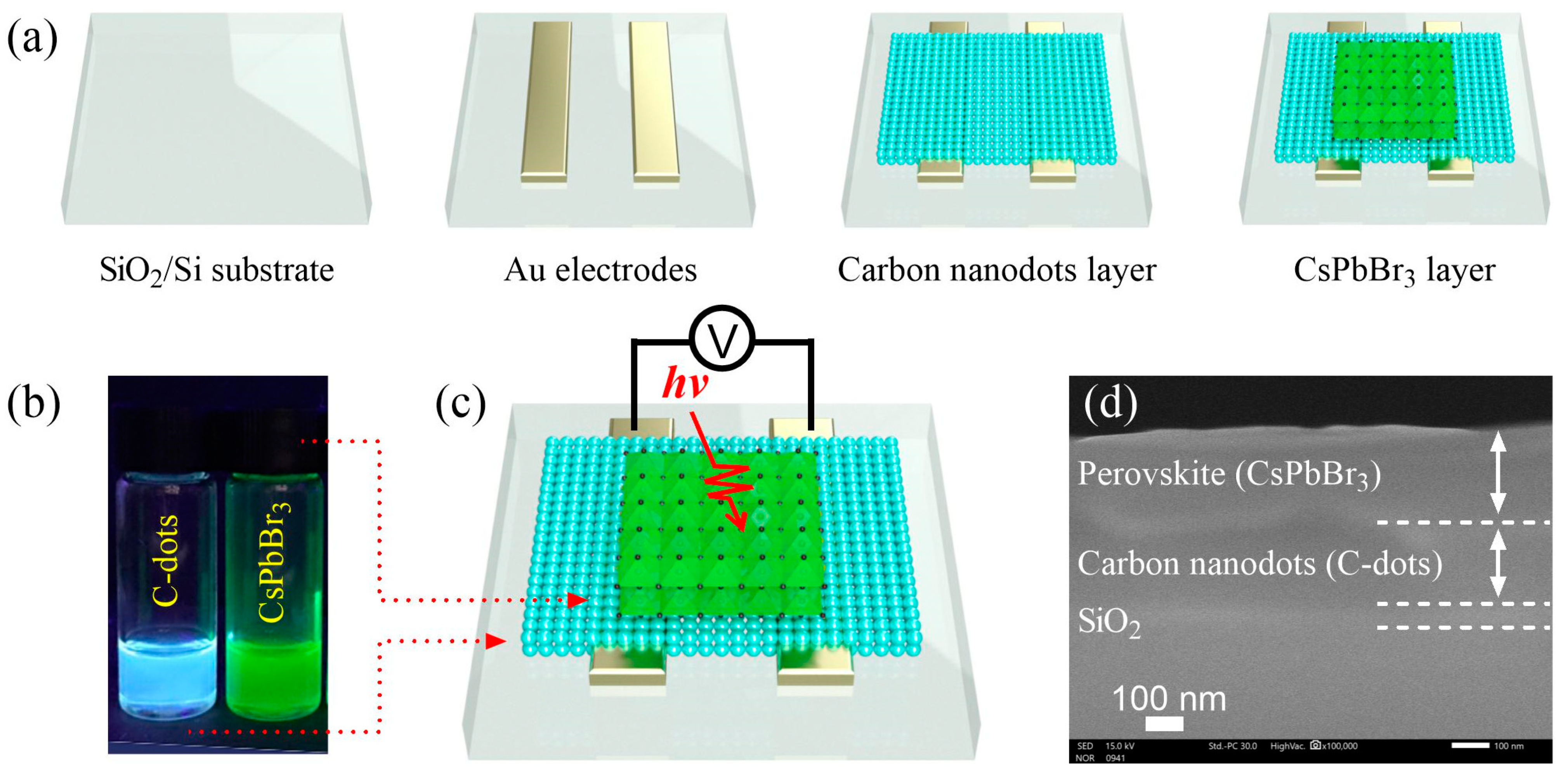
3.1. Structure and Fabrication of Photodetector Device

Figure 1a shows a schematic for the fabrication process of the C-dot/perovskite photodetector. Initially, Ti/Au (3/30 nm) were sputtered on a pre-cleaned commercial p-type Si substrate, with a 100 nm SiO2 oxide layer, using standard lithography and a wet etching process to obtain interdigitated electrodes with a total effective area of 0.0061 cm2. Then, a single layer of C-dots was deposited on top of the interdigitated electrodes by directly drop-casting the C-dot solution, and the whole substrate was pre-heated at 300 °C for 30 min to evaporate the solvent. Similarly, a perovskite layer was deposited on top the C-dot layer, and annealed at 100 °C for 15 min to complete the fabrication process of the C-dot/perovskite photodetector. The complete fabrication process of the fabricated photodetector is explained in detail in the experimental sections. Figure 1b shows an image of C nanodots and perovskite solutions, under 365 nm UV light, used for the fabrication process of the C nanodot/perovskite bilayer photodetector. The C nanodot and perovskite layers emitted typical light blue and green colors under 365 nm UV light. The same colors were used in constructing a full schematic structure of a C nanodot/perovskite device to distinguish between the C nanodot and perovskite layers as shown in Figure 1c.
The cross-sectional SEM image of the C nanodot/perovskite bilayer heterostructure photodetector is shown in Figure 1d. The C nanodot/perovskite bilayer heterostructure deposited on the Si substrate with the 100 nm SiO2 oxide layer is very obvious. The thicknesses of the C nanodot and perovskite layers were 380 and 420 nm, respectively. Moreover, the thickness of the C nanodot (380 nm) layer is much higher than that of the Ti/Au (3/30 nm) electrodes when ensuring that the perovskite layer (420 nm) was not in contact with the Ti/Au (3/30 nm) electrodes. This is very important to evaluate the carrier transport properties of the C nanodot layer in the C nanodot/perovskite device in the dark and under illumination conditions.

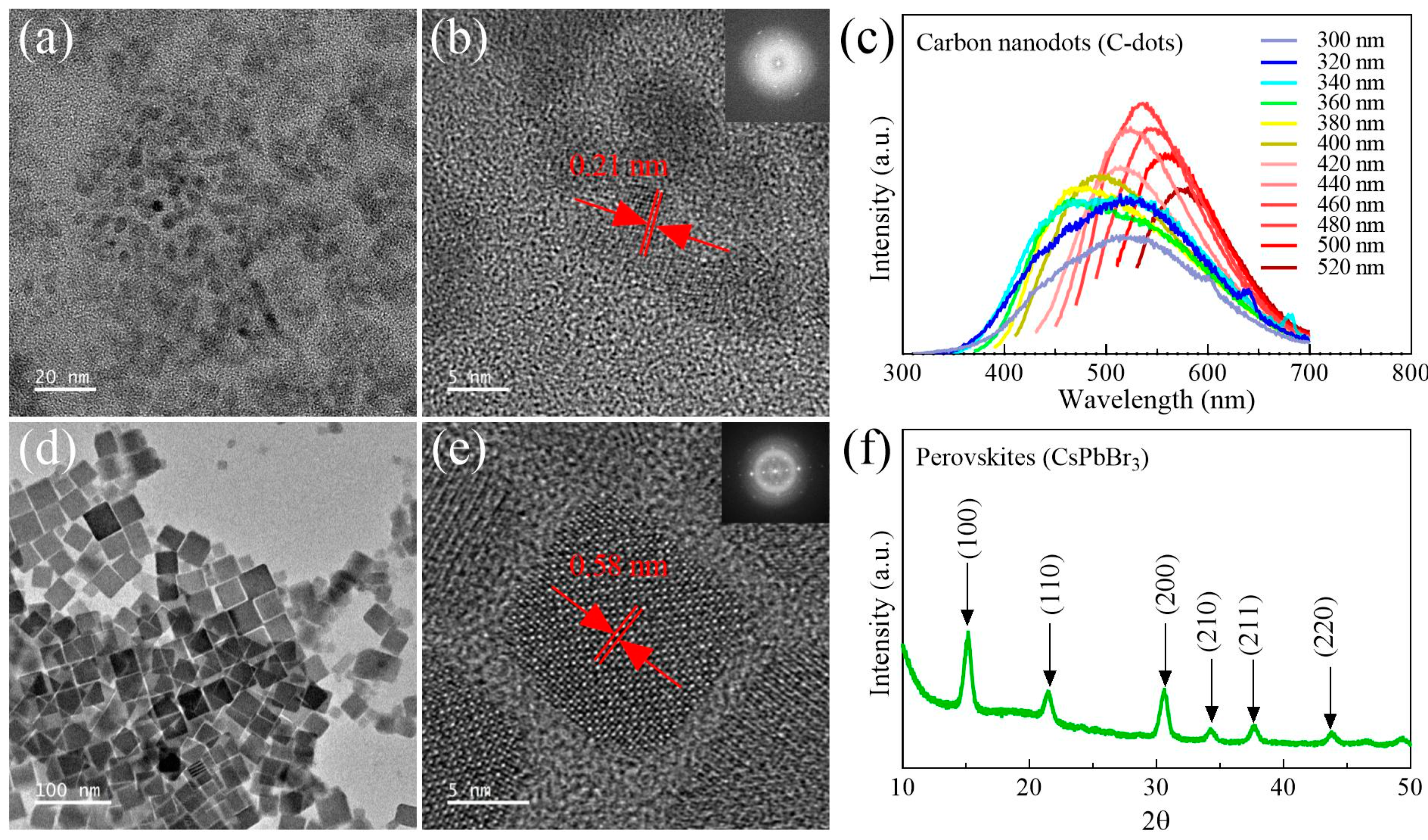
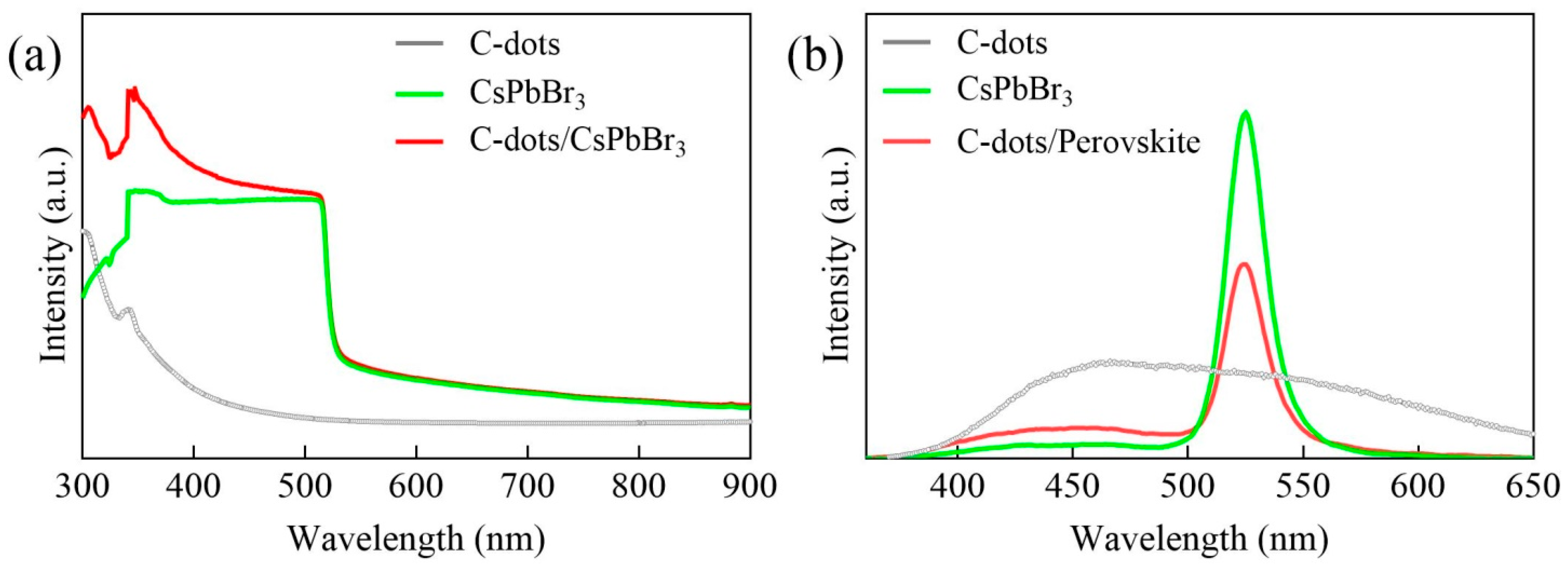
3.2. Characterizations and Properties of the Prepared Materials

The crystal structures and morphologies of carbon nanodots and perovskites are evaluated using transmission electron microscopy (TEM), X-ray diffraction (XRD), and a fluorescence spectrophotometer, as shown in Figure 2. The C nanodots are spherical in shape, stacked in layers, and narrowly distributed in size with an average size of 4.5 nm, as shown in Figure 2a. The high crystallinity of a typical C-dot structure, with a lattice fringe of 0.21 nm, is very clear in Figure 2b and the inset figure of Figure 2b [47,51]. The excitation-dependent photoluminescence behavior of the 0-dimensional (0D) C-dot solution is also confirmed by measuring its photoluminescence spectra (PL) at different excitation wavelengths from 300 to 520 nm, as shown in Figure 2c [51,52,53]. These results confirm a highly crystalline structure and the excitation-dependent photoluminescence properties of synthesized C-dots, as reported elsewhere. In addition, the CsPbBr3 perovskite structure is highly crystalline and cubic-shaped with an area of 17 nm × 17 nm, as shown in Figure 2d,e [23,54]. The high crystallinity and distinctive lattice fringe of 0.58 nm for the typical CsPbBr3 perovskite nanocrystals are shown in Figure 2e. The inset of Figure 2e demonstrates the selected area electron diffraction (SAED) pattern of the corresponding CsPbBr3 nanocrystals shown in Figure 2e, which further confirms the high crystallinity of the synthesized nanocrystals. Furthermore, the XRD spectra of the perovskites’ film exhibit peaks at 100, 110, 200, 210, 211, and 220, corresponding to the cubic structure of all-inorganic perovskite nanosheets, as shown in Figure 2f [9]. These results confirm a highly crystalline structure and good quality of the synthesized perovskite nanosheets, as reported elsewhere.
The optical characterizations of the C-dots, CsPbBr3 perovskites, and C-dot/CsPbBr3 perovskite layers were evaluated using UV–Vis and photoluminescence spectrophotometers, as presented in Figure 3. Figure 3a shows the absorption spectra of the C-dots, perovskites, and C-dot/perovskite layers. The C-dots have a narrow spectrum ranging from the ultraviolet -B to the ultraviolet-A region with an absorption peak at 343 nm, corresponding to a band gap of 3.61 eV [51,55], whereas the perovskites have a typical broad absorption spectrum ranging from the ultraviolet to the visible region with an absorption peak at 520 nm, corresponding to a band gap of 2.4 eV [9,23]. The absorption intensity of the perovskite is much higher than that of the C-dots due to the intrinsic strong optical absorption behavior of the perovskites [4,54]. Unsurprisingly, the C-dot/perovskite bilayer has a similar spectrum to that of the pure perovskite layer with an absorption peak at 520 nm, corresponding to a band gap of 2.4 eV. This is due to the fact that the absorption in the C-dot/perovskite bilayer is mostly carried out by the top layer of the perovskites, and the absorption intensity of the C-dots in the visible region is almost zero. This result confirms that the C-dot/perovskite bilayer structure has a band gap of 2.4 eV, which is similar to that of the perovskite. Figure 3b shows the photoluminescence spectra of the C-dots, perovskites, and C-dot/perovskite layers. The PL spectrum of the C-dot and perovskite layers exhibits a typical emission band at 434 nm [47,51,55] and 515 nm [9,23,48] after 365 nm excitation, respectively. Moreover, the PL spectrum of the C-dot/perovskite bilayer shows an emission band at 515 nm, which is similar to that of the perovskite but with 50% less PL intensity compared to the PL intensity of perovskites. This means that when the C-dot/perovskite bilayer structure was excited with a 365 nm wavelength, the top layer of the perovskite absorbed photons (a large number of electrons moved from its valance band to its conduction band) and emitted fewer photons (fewer electrons moved from its conduction band back to its valance band) because some of these electrons were transferred to the conduction band of the C-dot layer. The results indicate that the C-dots work as a photocarrier transport layer in the C-dot/perovskite bilayer structure, where the absorption and emission are mostly carried out by the top layer of the perovskite. These findings will be later confirmed by a detailed analysis of the energy band alignment of the C-dot/perovskite bilayer structure.

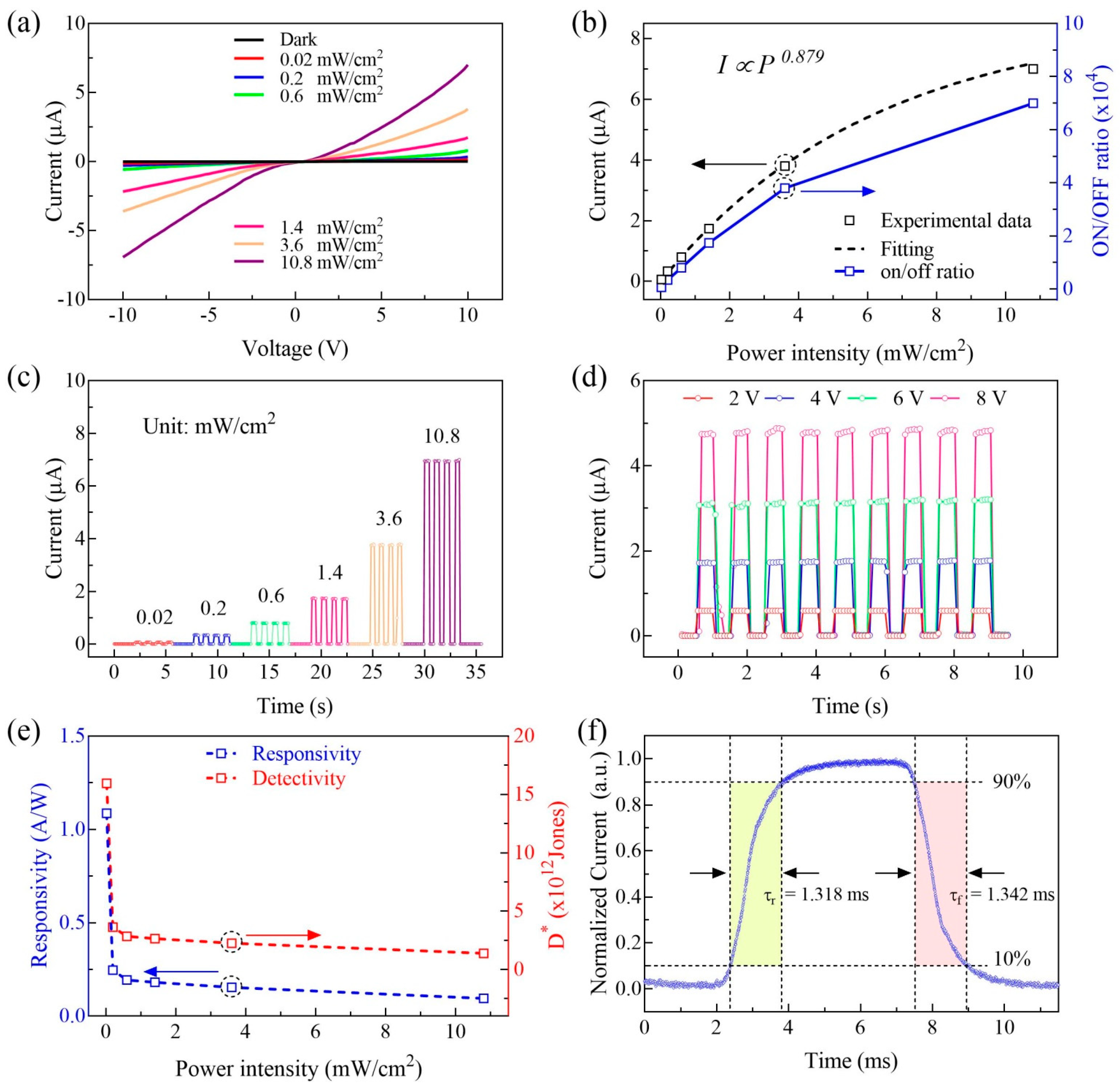
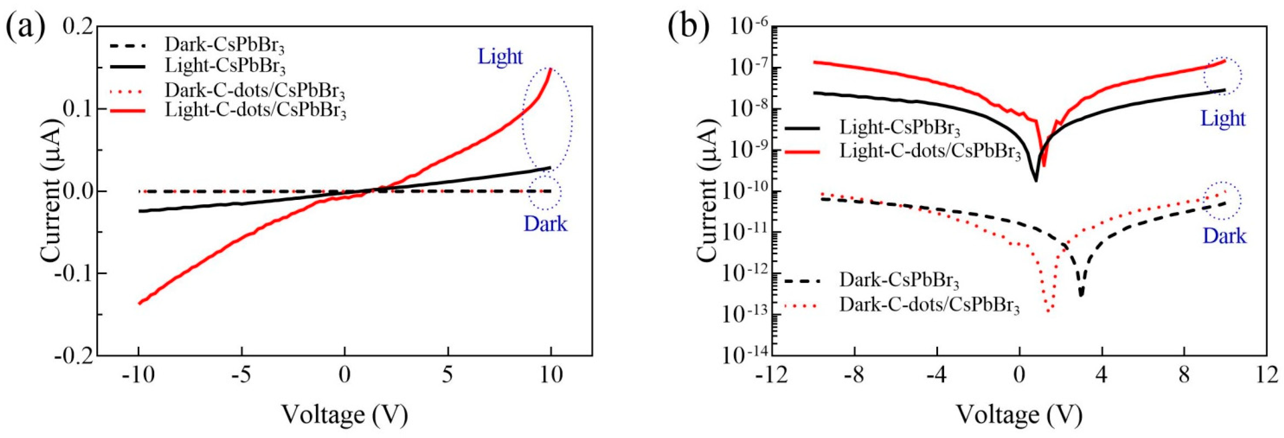
3.3. Performance of Fabricated Photodetector

Figure 4a shows the current–voltage (I–V) curves of the C-dot/perovskite photodetector in the dark and under a 520 nm light irradiation with different intensities ranging from 0.02 to 10.8 mW/cm2. The I–V curves are symmetrical, and the dark current (Id) is about 0.01 nA at 10 V bias voltage, which is an advantage for the photodetector [56,57]. When the laser intensity rose from 0.02 to 10.8 mW/cm2, the photocurrent (IPh) increased dramatically at both forward and reverse bias.
Figure 4b shows the photocurrent and the on/off ratio (i.e., photocurrent to dark current ratio) of the C-dot/perovskite photodetector as a function of light intensity at 10 V. The photocurrents increased from 0.15 to 6.93 µA when the laser intensity increased from 0.8 to 0.02 to 10.8 mW/cm2. This increase in photocurrent is due to the increase in the population of photoexcited electron–hole pairs at a higher intensity. The increased photocurrent due to the higher light intensity can be described by a power law according to the following equation [58]:
I p h P θ
The θ is the power law index, and it can be determined by fitting the experimental data of photocurrent values, as shown in Figure 4b. The θ value is 0.879 (0 < θ < 1), which indicates the existence of traps and defects in the C-dot/perovskite heterojunction photodetector [59,60,61]. This can also be confirmed by the light intensity-dependent calculated on/off ratio behavior in Figure 4b. The on/off ratio increased from 554 to 1500 when the light intensity increased from 0.02 to 10.8 mW/cm2. Furthermore, Figure 4c shows the pulsed driven current versus time (I–T) curves of the photodetector under 520 nm light illumination with different light intensities at 10 V bias voltage. The photodetector exhibits stable and reproducible pulse driven photocurrent values similar to that of the I–V curves when similar light intensities at 10 V bias voltage are applied. In addition, Figure 4d shows the pulse driven current versus time (I–T) curves of the photodetector under a 520 nm light illumination with a 10.8 mW/cm2 light intensity as a function of applied bias voltages. The photocurrent values are very stable and reproducible when the 520 nm laser with light intensity of 10.8 mW/cm2 and different applied bias voltages of 2, 4, 6, and 8 V are applied [21,22]. These photocurrent values are similar to that of the I–V curve when bias voltages of 2,4,6, and 8 V are applied. All of the above results confirm that the C nanodot/perovskite bilayer heterostructure PD is stable and promptly generated a photocurrent with a reproducible response in the on–off cycles. Furthermore, the stability of the C-dot/perovskite photodetector is due to the high stability of all-inorganic (CsPbBr3) perovskites in a humid environment, unlike organic–inorganic halide perovskites, such as Ch3NH3PbI3 [8,54,62]. Moreover, the C-dots used in the fabricated device are chemically doped with nitrogen during the synthesis process, and thus are highly stable as reported by [40,44,50].
The performance of the C-dot/perovskite PD was evaluated by calculating responsivity (R) and specific detectivity (D*) according to the following equations [26]:
R = I d I p h   P o p t × S
D * = A 1 / 2 × R   2   I d q  
where POpt is the laser intensity and q is the elementary charge, whereas the S and A are the effective illuminated and device areas, respectively. Figure 4e illustrates the responsivity and specific detectivity of the C-dot/perovskite PD as a function of light intensity at 10 V applied bias voltage.
The responsivity reached a maximum value of 1.09 A/W at a low light intensity of 0.02 mW/cm2 and decreased to a minimum value of 0.09 A/W at a higher light intensity of 10.8 mW/cm2. Similarly, the specific detectivity decreased from 1.593 × 10¹³ to 1.37 × 10¹² Jones when the light intensity was increased from 0.02 to 10.8 mW/cm2. It is widely known and theoretically putative that both responsivity and specific detectivity have the highest values at lower light intensities [54]. In addition, the performance of the C-dot/perovskite PD was evaluated by measuring the speed of the photodetector when illuminated with 0.08 mW/cm2 of light intensity and biased with 10 V. Figure 5f shows a single 10 (ms) period pulsed I–T curve with rise and fall times, indicated by two vertical black dashed lines around the yellow and red rectangles, respectively. The rise and decay times of the fabricated C-dot/perovskite bilayer heterojunction device are 1.318 and 1.342 ms, respectively. The rise time is faster than the fall time, which is a typical behavior for most perovskite heterojunction-based photodetectors [9,12,23]. The performance summary for the hybrid PD is shown in Table 1 as follows:
In addition, the performances of the pure perovskite (without carbon dots) and the hybrid (with carbon dots) PDs were compared by measuring the I–V curves for both devices, as shown in Figure 5a,b. The dark currents for both devices are 0.00005 and 0.0001 µA, respectively, while the photocurrent of the hybrid device was enhanced from 0.028 to 0.15 µA. By using the equations above, the performance summaries for the pure perovskite (without carbon dots) and the hybrid (with carbon dots) PDs are shown in Table 2. The responsivity (R) of the hybrid PD was enhanced from 0.209 to 1.09 A/W, which indicates that the carbon nanodot layer is able to enhance a perovskite-based optical device.
To understand the better properties of the C-dot/CsPbBr3 perovskite bilayer heterojunction photodetector, the performance of the fabricated bilayer heterojunction photodetector was compared with the other reported photodetectors reported in the literature and summarized in Table 3. The responsivity of the fabricated C-dot/perovskite bilayer photodetector (1.09 A/W) not only outperformed the responsivity of photodetectors based on single crystal CsPbBr3 (0.028A/W), graphene/GQDs/graphene (0.5 A/W), Au NP/CsPbBr3 NCs (0.01004 A/W), and TiO2 NC/CH3NH3PbI3 (0.12 A/W), but was also comparable to well-known 2D MoS2/CsPbBr3 (4.4 A/W) and WS2/CH3NH3PbI3 (2.1 A/W). Furthermore, the speed of the fabricated C-dot/perovskite bilayer photodetector (1.318/1.342 ms) is much faster than that of photodetectors based on the single crystal CsPbBr3 (90.7/57 ms), m-TiO2/CsPbBr3 QDs (>10,000 ms), TiO2 NC/CH3NH3PbI3 (490/560 ms), and 2D WS2/CH3NH3PbI3 (3000 ms).

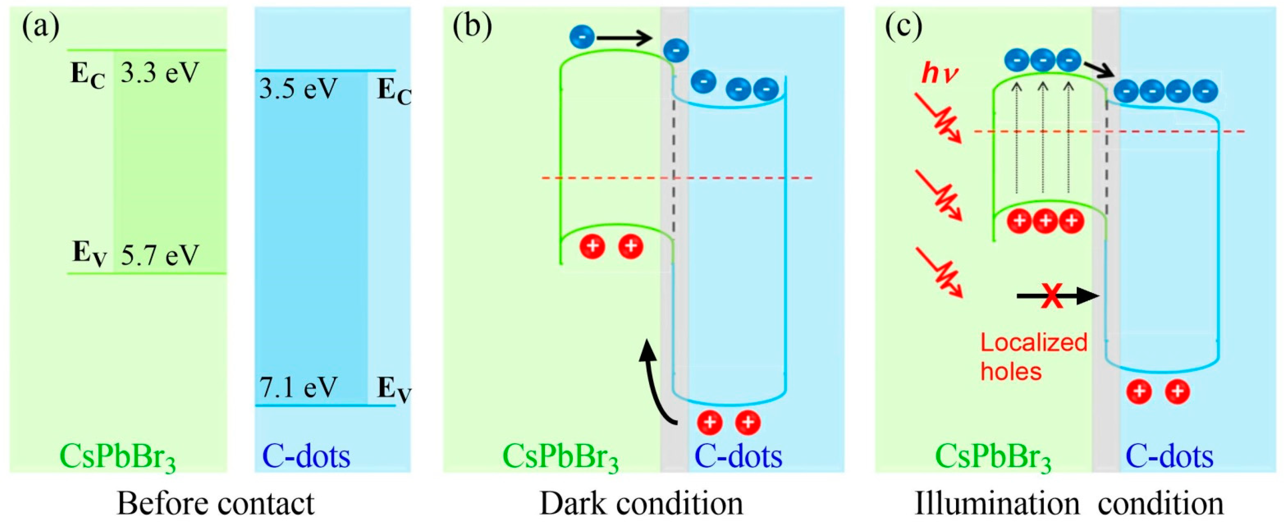
3.4. Mechanism for the Enhanced Performance of the Fabricated Heterojunction Photodetector

The working principle of the C-dot/CsPbBr3 perovskite heterojunction photodetector is explained based on the energy band alignment of C-dots and perovskite materials before contact, after contact in the dark, and under illumination conditions, as shown in Figure 6. Figure 6a shows the energy band alignment of C-dot and perovskite materials before contact. The conduction band and valence band levels for the perovskites are 3.3 and 5.7 eV, respectively [9,23,47]. Moreover, the conduction band and valence band levels for the C-dots are 3.5 and 7.1 eV, respectively [47,51,55]. Figure 6b shows the energy band alignment of the C-dot and perovskite materials after contact in the dark. The C-dot/perovskite interface heterojunction shows a type II band alignment with a band offset of 1.4 and 0.2 eV at the valence and conduction bands, respectively. Due to the difference in the work function of n-type C-dots and perovskite nanocrystals, a depletion region is formed at the interface, and thus, a built-in electrical field separates electron−hole pairs in the perovskite.
Figure 6c shows the energy band structure of C-dot and CsPbBr3 perovskite materials under illumination. The perovskite layer absorbs photons and, thus, a large number of electron–hole pairs are generated. The electrons in the conduction band of the perovskite layer are transferred to the conduction band of the C-dot layer by the built-in electric field, whereas the holes are blocked in the perovskites, due to the large valance band level of the C-dot layer. Due to this, the Fermi level of the C-dot layer and perovskite layer are raised and lowered, respectively, and the Schottky barrier height between the C-dots and Au electrode is reduced [9,15,23]. This allows only electrons to be re-circulated to the outside of the device, without recombining with the blocked holes, leading to a higher photocurrent, responsivity, and detectivity in the C-dot/perovskite bilayer heterojunction photodetector. In a few words, the efficient charge separation and transport at the C-dot/perovskite interface is the main reason behind the performance enhancement for the C-dot/perovskite bilayer heterojunction photodetector. This finding may pave the way for enhancing perovskite-based optoelectronics with carbon nanodots similar to other reported heterojunction-based optical devices [70,71,72,73].

4. Conclusions

In summary, a low-cost and simple drop-casting method was used to fabricate a UV–Vis photodetector based on a C-dot/CsPbBr3 perovskite bilayer heterojunction. The fabricated photodetector shows a responsivity of 1.09 A/W, a specific detectivity of 1.593 × 10¹³ Jones, and an on/off ratio of 1.5 × 10³. In addition, the photodetector exhibits a fast rise and decay time of 1.318/1.342 µs and a highly stable photocurrent of 6.97 µA. The performance of the C-dot/CsPbBr3 perovskite bilayer heterojunction is much better than most reported perovskite photodetectors.

Author Contributions

H.A. (Hassan Algadi) and A.U.: experiment conduction, data analysis, original manuscript drafting, writing—review and editing; H.A. (Hassan Algadi), A.U., H.A. (Hasan Algadi), T.A., and S.B.: visualization, editing, revision, and validation. All authors have read and agreed to the published version of the manuscript.

Funding

The authors would like to acknowledge the support of the Deputy for Research and Innovation—Ministry of Education, Kingdom of Saudi Arabia for the research grant (NU/IFC/INT/01/004) under the institutional funding committee at Najran University, Kingdom of Saudi Arabia.

Institutional Review Board Statement

Not applicable.

Informed Consent Statement

Not applicable.

Data Availability Statement

Data is contained within the article.

Conflicts of Interest

The authors have no conflict of interest to declare that is relevant to the content of this article.

References

  1. Hao, D.; Zou, J.; Huang, J. Recent developments in flexible photodetectors based on metal halide perovskite. InfoMat 2019, 2, 139–169. [Google Scholar] [CrossRef] [Green Version]
  2. Leung, S.-F.; Ho, K.T.; Kung, P.-K.; Hsiao, V.K.S.; Alshareef, H.N.; Wang, Z.L.; He, J.-H. A Self-Powered and Flexible Organometallic Halide Perovskite Photodetector with Very High Detectivity. Adv. Mater. 2018, 30, 1704611. [Google Scholar] [CrossRef] [PubMed]
  3. Zhang, F.; Zhong, H.; Chen, C.; Wu, X.; Hu, X.; Huang, H.; Han, J.; Zou, B.; Dong, Y. Brightly Luminescent and Color-Tunable Colloidal CH3NH3PbX3 (X = Br, I, Cl) Quantum Dots: Potential Alternatives for Display Technology. ACS Nano 2015, 9, 4533–4542. [Google Scholar] [CrossRef] [PubMed]
  4. Adinolfi, V.; Peng, W.; Walters, G.; Bakr, O.M.; Sargent, E.H. The Electrical and Optical Properties of Organometal Halide Perovskites Relevant to Optoelectronic Performance. Adv. Mater. 2018, 30, 1–13. [Google Scholar] [CrossRef] [PubMed]
  5. Dong, Q.; Fang, Y.; Shao, Y.; Mulligan, P.; Qiu, J.; Cao, L.; Huang, J. Electron-hole diffusion lengths > 175 μm in solution-grown CH3NH3PbI3single crystals. Science 2015, 347, 967–970. [Google Scholar] [CrossRef] [PubMed] [Green Version]
  6. Wehrenfennig, C.; Eperon, G.E.; Johnston, M.; Snaith, H.J.; Herz, L.M. High Charge Carrier Mobilities and Lifetimes in Organolead Trihalide Perovskites. Adv. Mater. 2014, 26, 1584–1589. [Google Scholar] [CrossRef] [Green Version]
  7. Yang, W.S.; Park, B.-W.; Jung, E.H.; Jeon, N.J.; Kim, Y.C.; Lee, D.U.; Shin, S.S.; Seo, J.; Kim, E.K.; Noh, J.H.; et al. Iodide management in formamidinium-lead-halide–based perovskite layers for efficient solar cells. Science 2017, 356, 1376–1379. [Google Scholar] [CrossRef] [Green Version]
  8. Yang, D.; Cao, M.; Zhong, Q.; Li, P.; Zhang, X.; Zhang, Q. All-inorganic cesium lead halide perovskite nanocrystals: Synthesis, surface engineering and applications. J. Mater. Chem. C 2019, 7, 757–789. [Google Scholar] [CrossRef]
  9. Dong, Y.; Gu, Y.; Zou, Y.; Song, J.; Xu, L.; Li, J.; Xue, J.; Li, X.; Zeng, H. Improving All-Inorganic Perovskite Photodetectors by Preferred Orientation and Plasmonic Effect. Small 2016, 12, 5622–5632. [Google Scholar] [CrossRef]
  10. Li, X.; Yu, D.; Cao, F.; Gu, Y.; Wei, Y.; Wu, Y.; Song, J.; Zeng, H. Healing All-Inorganic Perovskite Films via Recyclable Dissolution-Recyrstallization for Compact and Smooth Carrier Channels of Optoelectronic Devices with High Stability. Adv. Funct. Mater. 2016, 26, 5903–5912. [Google Scholar] [CrossRef]
  11. Li, X.; Yu, D.; Chen, J.; Wang, Y.; Cao, F.; Wei, Y.; Wu, Y.; Wang, L.; Zhu, Y.; Sun, Z.; et al. Constructing Fast Carrier Tracks into Flexible Perovskite Photodetectors To Greatly Improve Responsivity. ACS Nano 2017, 11, 2015–2023. [Google Scholar] [CrossRef] [PubMed]
  12. Yi, X.; Ren, Z.; Chen, N.; Li, C.; Zhong, X.; Yang, S.; Wang, J. TiO2 Nanocrystal/Perovskite Bilayer for High-Performance Photodetectors. Adv. Electron. Mater. 2017, 3, 1700251. [Google Scholar] [CrossRef] [Green Version]
  13. Zhou, L.; Yu, K.; Yang, F.; Zheng, J.; Zuo, Y.; Li, C.; Cheng, B.; Wang, Q. All-inorganic perovskite quantum dot/mesoporous TiO2 composite-based photodetectors with enhanced performance. Dalton Trans. 2016, 46, 1766–1769. [Google Scholar] [CrossRef]
  14. Zhou, L.; Yu, K.; Yang, F.; Cong, H.; Wang, N.; Zheng, J.; Zuo, Y.; Li, C.; Cheng, B.; Wang, Q. Insight into the effect of ligand-exchange on colloidal CsPbBr3 perovskite quantum dot/mesoporous-TiO2composite-based photodetectors: Much faster electron injection. J. Mater. Chem. C 2017, 5, 6224–6233. [Google Scholar] [CrossRef]
  15. Liu, H.; Zhang, X.; Zhang, L.; Yin, Z.; Wang, D.; Meng, J.; Jiang, Q.; Wang, Y.; You, J. A high-performance photodetector based on an inorganic perovskite–ZnO heterostructure. J. Mater. Chem. C 2017, 5, 6115–6122. [Google Scholar] [CrossRef]
  16. Dang, V.Q.; Han, G.S.; Trung, T.Q.; Duy, L.T.; Jin, Y.-U.; Hwang, B.-U.; Jung, H.-S.; Lee, N.-E. Methylammonium lead iodide perovskite-graphene hybrid channels in flexible broadband phototransistors. Carbon 2016, 105, 353–361. [Google Scholar] [CrossRef]
  17. Spina, M.; Lehmann, M.; Náfrádi, B.; Bernard, L.S.; Bonvin, E.; Gaál, R.; Magrez, A.; Forró, L.; Horváth, E. Microengineered CH3NH3PbI3Nanowire/Graphene Phototransistor for Low-Intensity Light Detection at Room Temperature. Small 2015, 11, 4824–4828. [Google Scholar] [CrossRef] [Green Version]
  18. Lee, Y.; Kwon, J.; Hwang, E.; Ra, C.-H.; Yoo, W.J.; Ahn, J.-H.; Park, J.H.; Cho, J.H. High-Performance Perovskite-Graphene Hybrid Photodetector. Adv. Mater. 2015, 27, 41–46. [Google Scholar] [CrossRef]
  19. Wang, Y.; Zhang, Y.; Lu, Y.; Xu, W.; Mu, H.; Chen, C.; Qiao, H.; Song, J.; Li, S.; Sun, B.; et al. Hybrid Graphene-Perovskite Phototransistors with Ultrahigh Responsivity and Gain. Adv. Opt. Mater. 2015, 3, 1389–1396. [Google Scholar] [CrossRef]
  20. Kwak, D.-H.; Lim, D.-H.; Ra, H.-S.; Ramasamy, P.; Lee, J.-S. High performance hybrid graphene–CsPbBr3−xIx perovskite nanocrystal photodetector. RSC Adv. 2016, 6, 65252–65256. [Google Scholar] [CrossRef]
  21. Ma, C.; Shi, Y.; Hu, W.; Chiu, M.-H.; Liu, Z.; Bera, A.; Li, F.; Wang, H.; Li, L.; Wu, T. Heterostructured WS2/CH3NH3PbI3 Photoconductors with Suppressed Dark Current and Enhanced Photodetectivity. Adv. Mater. 2016, 28, 3683–3689. [Google Scholar] [CrossRef]
  22. Lu, J.; Carvalho, A.; Liu, H.; Lim, S.X.; Neto, A.H.C.; Sow, C.H. Hybrid Bilayer WSe2-CH3NH3PbI3Organolead Halide Perovskite as a High-Performance Photodetector. Angew. Chem. Int. Ed. 2016, 55, 11945–11949. [Google Scholar] [CrossRef]
  23. Song, X.; Liu, X.; Yu, D.; Huo, C.; Ji, J.; Li, X.; Zhang, S.; Zou, Y.; Zhu, G.; Wang, Y.; et al. Boosting Two-Dimensional MoS2/CsPbBr3 Photodetectors via Enhanced Light Absorbance and Interfacial Carrier Separation. ACS Appl. Mater. Interfaces 2018, 10, 2801–2809. [Google Scholar] [CrossRef]
  24. Wang, Y.; Fullon, R.; Acerce, M.; Petoukhoff, C.E.; Yang, J.; Chen, C.; Du, S.; Lai, S.K.; Lau, S.P.; Voiry, D.; et al. Solution-Processed MoS2/Organolead Trihalide Perovskite Photodetectors. Adv. Mater. 2016, 29, 1603995. [Google Scholar] [CrossRef] [PubMed]
  25. Shi, E.; Gao, Y.; Finkenauer, B.P.; Akriti, A.; Coffey, A.H.; Dou, L. Two-dimensional halide perovskite nanomaterials and heterostructures. Chem. Soc. Rev. 2018, 47, 6046–6072. [Google Scholar] [CrossRef]
  26. Mei, F.; Sun, D.; Mei, S.; Feng, J.; Zhou, Y.; Xu, J. Advances in Physics: X Recent progress in perovskite-based photodetectors: The design of materials and structures. Adv. Phys. X 2019, 4, 1592709. [Google Scholar]
  27. Wang, J.; Han, J.; Chen, X.; Wang, X. Design strategies for two-dimensional material photodetectors to enhance device performance. InfoMat 2019, 1, 33–53. [Google Scholar] [CrossRef]
  28. Lee, S.; Shin, S.; Lee, S.; Seo, J.; Lee, J.; Son, S.; Cho, H.J.; Algadi, H.; Al-Sayari, S.; Kim, D.E.; et al. Stretchable Electronics: Ag Nanowire Reinforced Highly Stretchable Conductive Fibers for Wearable Electronics. Adv. Funct. Mater. 2015, 25, 3105. [Google Scholar] [CrossRef] [Green Version]
  29. Lee, S.; Shin, S.; Lee, S.; Seo, J.; Lee, J.; Son, S.; Cho, H.J.; Algadi, H.; Al-Sayari, S.; Kim, D.E.; et al. Ag Nanowire Reinforced Highly Stretchable Conductive Fibers for Wearable Electronics. Adv. Funct. Mater. 2015, 25, 3114–3121. [Google Scholar] [CrossRef]
  30. Lee, J.; Yoon, J.; Kim, H.G.; Kang, S.; Oh, W.-S.; Algadi, H.; Al-Sayari, S.; Shong, B.; Kim, S.-H.; Kim, H.; et al. Highly conductive and flexible fiber for textile electronics obtained by extremely low-temperature atomic layer deposition of Pt. NPG Asia Mater. 2016, 8, e331. [Google Scholar] [CrossRef] [Green Version]
  31. Kang, S.; Lee, J.; Lee, S.; Kim, S.; Kim, J.-K.; Algadi, H.; Al-Sayari, S.; Kim, D.; Kim, D.; Lee, T. Highly Sensitive Pressure Sensor Based on Bioinspired Porous Structure for Real-Time Tactile Sensing. Adv. Electron. Mater. 2016, 2, 1600356. [Google Scholar] [CrossRef]
  32. Kang, S.; Lee, J.; Lee, S.; Kim, S.; Kim, J.-K.; Algadi, H.; Al-Sayari, S.; Kim, D.-E.; Lee, T. Pressure Sensors: Highly Sensitive Pressure Sensor Based on Bioinspired Porous Structure for Real-Time Tactile Sensing. Adv. Electron. Mater. 2016, 2, 1600356. [Google Scholar] [CrossRef]
  33. Sahoo, B.N.; Woo, J.; Algadi, H.; Lee, J.; Lee, T. Superhydrophobic, Transparent, and Stretchable 3D Hierarchical Wrinkled Film-Based Sensors for Wearable Applications. Adv. Mater. Technol. 2019, 4, 1900230. [Google Scholar] [CrossRef]
  34. Mahata, C.; Algadi, H.; Lee, J.; Kim, S.; Lee, T. Biomimetic-inspired micro-nano hierarchical structures for capacitive pressure sensor applications. Measurement 2020, 151, 107095. [Google Scholar] [CrossRef]
  35. Xie, C.; Nie, B.; Zeng, L.; Liang, F.-X.; Wang, M.-Z.; Luo, L.; Feng, M.; Yu, Y.; Wu, C.-Y.; Wu, Y.; et al. Core–Shell Heterojunction of Silicon Nanowire Arrays and Carbon Quantum Dots for Photovoltaic Devices and Self-Driven Photodetectors. ACS Nano 2014, 8, 4015–4022. [Google Scholar] [CrossRef]
  36. Guo, D.-Y.; Shan, C.-X.; Qu, S.-N.; Shen, D.-Z. Highly Sensitive Ultraviolet Photodetectors Fabricated from ZnO Quantum Dots/Carbon Nanodots Hybrid Films. Sci. Rep. 2014, 4, 7469. [Google Scholar] [CrossRef] [Green Version]
  37. Huang, C.-Y.; Chen, M.-L.; Yu, C.-W.; Wan, T.-C.; Chen, S.-H.; Chang, C.-Y.; Hsu, T.-Y. Dual functional photo-response for p-Si/SiO2/n-InGaZnO graphene nanocomposites photodiodes. Nanotechnology 2018, 29, 505202. [Google Scholar] [CrossRef]
  38. Huang, C.Y.; Kang, C.C.; Ma, Y.C.; Chou, Y.C.; Ye, J.H.; Huang, R.T.; Siao, C.Z.; Lin, Y.C.; Chang, Y.H.; Shen, J.L.; et al. P-GaN/n-ZnO nanorods: The use of graphene nanosheets composites to increase charge separation in self-powered visible-blind UV photodetectors. Nanotechnology 2018, 29, 445201. [Google Scholar] [CrossRef] [PubMed]
  39. Dai, M.-K.; Lian, J.-T.; Lin, T.-Y.; Chen, Y.-F. High-performance transparent and flexible inorganic thin film transistors: A facile integration of graphene nanosheets and amorphous InGaZnO. J. Mater. Chem. C 2013, 1, 5064–5071. [Google Scholar] [CrossRef]
  40. Do, S.; Kwon, W.; Rhee, S.-W. Soft-template synthesis of nitrogen-doped carbon nanodots: Tunable visible-light photoluminescence and phosphor-based light-emitting diodes. J. Mater. Chem. C 2014, 2, 4221. [Google Scholar] [CrossRef] [Green Version]
  41. Zhang, X.; Zhang, Y.; Wang, Y.; Kalytchuk, S.; Kershaw, S.V.; Wang, Y.; Wang, P.; Zhang, T.; Zhao, Y.; Zhang, H.; et al. Color-Switchable Electroluminescence of Carbon Dot Light-Emitting Diodes. ACS Nano 2013, 7, 11234–11241. [Google Scholar] [CrossRef]
  42. Wang, F.; Chen, Y.-H.; Liu, C.-Y.; Ma, D.-G. White light-emitting devices based on carbon dots’ electroluminescence. Chem. Commun. 2011, 47, 3502–3504. [Google Scholar] [CrossRef] [PubMed]
  43. Baker, S.N.; Baker, G.A. Luminescent Carbon Nanodots: Emergent Nanolights. Angew. Chem. Int. Ed. 2010, 49, 6726–6744. [Google Scholar] [CrossRef]
  44. Chen, Q.; Wang, Y.; Wang, Y.; Zhang, X.; Duan, D.; Fan, C. Nitrogen-doped carbon quantum dots/Ag3PO4 complex photocatalysts with enhanced visible light driven photocatalytic activity and stability. J. Colloid Interface Sci. 2017, 491, 238–245. [Google Scholar] [CrossRef]
  45. Sánchez, R.S.; De La Fuente, M.S.; Suarez, I.; Muñoz-Matutano, G.; Martinez-Pastor, J.P.; Mora-Sero, I. Tunable light emission by exciplex state formation between hybrid halide perovskite and core/shell quantum dots: Implications in advanced LEDs and photovoltaics. Sci. Adv. 2016, 2, e1501104. [Google Scholar] [CrossRef] [Green Version]
  46. Fang, X.; Ding, J.; Yuan, N.; Sun, P.; Lv, M.; Ding, G.; Zhu, C. Graphene quantum dot incorporated perovskite films: Passivating grain boundaries and facilitating electron extraction. Phys. Chem. Chem. Phys. 2017, 19, 6057–6063. [Google Scholar] [CrossRef]
  47. Algadi, H.; Mahata, C.; Woo, J.; Lee, M.; Kim, M.; Lee, T. Enhanced Photoresponsivity of All-Inorganic (CsPbBr3) Perovskite Nanosheets Photodetector with Carbon Nanodots (CDs). Electronics 2019, 8, 678. [Google Scholar] [CrossRef] [Green Version]
  48. Algadi, H.; Mahata, C.; Sahoo, B.; Kim, M.; Koh, W.-G.; Lee, T. Facile method for the preparation of high-performance photodetectors with a GQDs/perovskite bilayer heterostructure. Org. Electron. 2020, 76, 105444. [Google Scholar] [CrossRef]
  49. Zhang, Q.; Jie, J.; Diao, S.; Shao, Z.; Zhang, Q.; Wang, L.; Deng, W.; Hu, W.; Xia, H.; Yuan, X.; et al. Solution-Processed Graphene Quantum Dot Deep-UV Photodetectors. ACS Nano 2015, 9, 1561–1570. [Google Scholar] [CrossRef] [PubMed]
  50. Ghosh, D.; Sarkar, K.; Devi, P.; Kim, K.-H.; Kumar, P. Current and future perspectives of carbon and graphene quantum dots: From synthesis to strategy for building optoelectronic and energy devices. Renew. Sustain. Energy Rev. 2021, 135, 110391. [Google Scholar] [CrossRef]
  51. Barman, M.K.; Mitra, P.; Bera, R.; Das, S.; Pramanik, A.; Parta, A. An efficient charge separation and photocurrent generation in the carbon dot–zinc oxide nanoparticle composite. Nanoscale 2017, 9, 6791–6799. [Google Scholar] [CrossRef] [PubMed]
  52. Farshbaf, M.; Davaran, S.; Rahimi, F.; Annabi, N.; Salehi, R.; Akbarzadeh, A. Carbon quantum dots: Recent progresses on synthesis, surface modification and applications. Artif. Cells Nanomed. Biotechnol. 2018, 46, 1331–1348. [Google Scholar] [CrossRef] [PubMed]
  53. Sciortino, A.; Cannizzo, A.; Messina, F. Carbon Nanodots: A Review—From the Current Understanding of the Fundamental Photophysics to the Full Control of the Optical Response. C J. Carbon Res. 2018, 4, 67. [Google Scholar] [CrossRef] [Green Version]
  54. Li, C.; Huang, W.; Gao, L.; Wang, H.; Hu, L.; Chen, T.; Zhang, H. Recent advances in solution-processed photodetectors based on inorganic and hybrid photo-active materials. Nanoscale 2020, 12, 2201–2227. [Google Scholar] [CrossRef] [PubMed]
  55. Barman, M.K.; Paramanik, B.; Bain, D.; Patra, A. Light Harvesting and White-Light Generation in a Composite of Carbon Dots and Dye-Encapsulated BSA-Protein-Capped Gold Nanoclusters. Chem. A Eur. J. 2016, 22, 11699–11705. [Google Scholar] [CrossRef]
  56. Luo, X.; Zhao, F.; Du, L.; Lv, W.; Xu, K.; Peng, Y.; Wang, Y.; Lu, F. Ultrasensitive flexible broadband photodetectors achieving pA scale dark current. NPJ Flex. Electron. 2017, 1, 1–7. [Google Scholar] [CrossRef]
  57. Dong, Y.; Zou, Y.; Song, J.; Song, X.; Zeng, H. Recent progress of metal halide perovskite photodetectors. J. Mater. Chem. C 2017, 5, 11369–11394. [Google Scholar] [CrossRef]
  58. Zeng, L.; Chen, Q.; Zhang, Z.; Wu, D.; Yuan, H.; Li, Y.; Qarony, W.; Lau, S.P.; Luo, L.; Tsang, Y.H. Multilayered PdSe2/Perovskite Schottky Junction for Fast, Self-Powered, Polarization-Sensitive, Broadband Photodetectors, and Image Sensor Application. Adv. Sci. 2019, 6, 1901134. [Google Scholar] [CrossRef] [PubMed] [Green Version]
  59. Wu, E.; Wu, D.; Jia, C.; Wang, Y.; Yuan, H.; Zeng, L.; Xu, T.; Shi, Z.; Tian, Y.; Li, X.J. In Situ Fabrication of 2D WS2/Si Type-II Heterojunction for Self-Powered Broadband Photodetector with Response up to Mid-Infrared. ACS Photonics 2019, 6, 565–572. [Google Scholar] [CrossRef] [Green Version]
  60. Zeng, L.-H.; Wang, M.-Z.; Hu, H.; Nie, B.; Yu, Y.-Q.; Wu, C.-Y.; Wang, L.; Hu, J.-G.; Xie, C.; Liang, F.-X.; et al. Monolayer Graphene/Germanium Schottky Junction As High-Performance Self-Driven Infrared Light Photodetector. ACS Appl. Mater. Interfaces 2013, 5, 9362–9366. [Google Scholar] [CrossRef]
  61. Zeng, L.; Lin, S.; Lou, Z.; Yuan, H.; Long, H.; Li, Y.; Lu, W.; Lau, S.P.; Wu, D.; Tsang, Y.H. Ultrafast and sensitive photodetector based on a PtSe2/silicon nanowire array heterojunction with a multiband spectral response from 200 to 1550 nm. NPG Asia Mater. 2018, 10, 352–362. [Google Scholar] [CrossRef] [Green Version]
  62. Yettapu, G.R.; Talukdar, D.; Sarkar, S.; Swarnkar, A.; Nag, A.; Ghosh, P.; Mandal, P. Terahertz Conductivity within Colloidal CsPbBr3 Perovskite Nanocrystals: Remarkably High Carrier Mobilities and Large Diffusion Lengths. Nano Lett. 2016, 16, 4838–4848. [Google Scholar] [CrossRef] [PubMed]
  63. Tang, L.; Ji, R.; Li, X.; Bai, G.; Liu, C.P.; Hao, J.; Lin, J.; Jiang, H.; Teng, K.S.; Yang, Z.; et al. Deep Ultraviolet to Near-Infrared Emission and Photoresponse in Layered N-Doped Graphene Quantum Dots. ACS Nano 2014, 8, 6312–6320. [Google Scholar] [CrossRef] [PubMed]
  64. Kim, C.O.; Hwang, S.W.; Kim, S.; Shin, D.H.; Kang, S.S.; Kim, J.M.; Jang, C.W.; Kim, J.H.; Lee, K.W.; Choi, S.-H.; et al. High-performance graphene-quantum-dot photodetectors. Sci. Rep. 2014, 4, 5603. [Google Scholar] [CrossRef] [Green Version]
  65. Ding, J.; Du, S.; Zuo, Z.; Zhao, Y.; Cui, H.; Zhan, X. High Detectivity and Rapid Response in Perovskite CsPbBr3 Single-Crystal Photodetector. J. Phys. Chem. C 2017, 121, 4917–4923. [Google Scholar] [CrossRef]
  66. Cha, J.-H.; Han, J.H.; Yin, W.; Park, C.; Park, Y.; Ahn, T.K.; Cho, J.H.; Jung, D.-Y. Photoresponse of CsPbBr3 and Cs4PbBr6 Perovskite Single Crystals. J. Phys. Chem. Lett. 2017, 8, 565–570. [Google Scholar] [CrossRef]
  67. Song, J.; Xu, L.; Li, J.; Xue, J.; Dong, Y.; Li, X.; Zeng, H. Monolayer and Few-Layer All-Inorganic Perovskites as a New Family of Two-Dimensional Semiconductors for Printable Optoelectronic Devices. Adv. Mater. 2016, 28, 4861–4869. [Google Scholar] [CrossRef] [PubMed]
  68. Chen, J.; Fu, Y.; Samad, L.; Dang, L.; Zhao, Y.; Shen, S.; Guo, L.; Jin, S. Vapor-Phase Epitaxial Growth of Aligned Nanowire Networks of Cesium Lead Halide Perovskites (CsPbX3, X = Cl, Br, I). Nano Lett. 2017, 17, 460–466. [Google Scholar] [CrossRef] [PubMed]
  69. Li, Y.; Shi, Z.-F.; Li, S.; Lei, L.-Z.; Ji, H.-F.; Wu, D.; Xu, T.-T.; Tian, Y.-T.; Li, X.-J. High-performance perovskite photodetectors based on solution-processed all-inorganic CsPbBr3 thin films. J. Mater. Chem. C 2017, 5, 8355–8360. [Google Scholar] [CrossRef]
  70. Larciprete, M.C.; Bosco, A.; Belardini, A.; Voti, R.L.; Leahu, G.; Sibilia, C.; Fazio, E.; Ostuni, R.; Bertolotti, M.; Passaseo, A.; et al. Blue second harmonic generation from aluminum nitride films deposited onto silicon by sputtering technique. J. Appl. Phys. 2006, 100, 023507. [Google Scholar] [CrossRef]
  71. Cesarini, G.; Leahu, G.; Grilli, M.L.; Sytchkova, A.; Sibilia, C.; Voti, R.L. Optical and photoacoustic investigation of AZO/Ag/AZO transparent conductive coating for solar cells. Phys. Status Solidi C. 2016, 13, 998–1001. [Google Scholar] [CrossRef]
  72. Lamastra, F.R.; Grilli, M.L.; Leahu, G.; Belardini, A.; Voti, R.L.; Sibilia, C.; Salvatori, D.; Cacciotti, I.; Nanni, F. Diatom frustules decorated with zinc oxide nanoparticles for enhanced optical properties. Nanotechnol. 2017, 28, 375704. [Google Scholar] [CrossRef] [PubMed]
  73. Lamastra, F.R.; Grilli, M.L.; Leahu, G.; Belardini, A.; Voti, R.L.; Sibilia, C.; Salvatori, D.; Cacciotti, I.; Nanni, F. Photoacoustic Spectroscopy Investigation of Zinc Oxide/Diatom Frustules Hybrid Powders. Int. J. Thermophys. 2018, 39, 1–10. [Google Scholar] [CrossRef]
Figure 1. (a) A schematic for the fabrication process of C-dot/perovskite heterostructure PD. (b) An image of C-dot and CsPbBr3 perovskite solutions under 365 nm UV light illumination. (c) A schematic structure of C-dot/CsPbBr3 perovskite heterostructure PD. (d) A cross-sectional image of C-dot/CsPbBr3 perovskite bilayer heterostructure deposited on a Si substrate with a 100 nm SiO2 oxide layer.
Crystals 11 00717 g001
Figure 2. (a) Low-magnification TEM image of carbon nanodots. (b) High-resolution TEM image of typical C-dots. (c) PL spectra of C-dots under different excitation wavelengths. (d) TEM image of the CsPbBr3 perovskite. (e) High-resolution TEM image of typical CsPbBr3 perovskite nanocrystals. (f) XRD pattern of the perovskite layer.
Crystals 11 00717 g002
Figure 3. (a) Absorption spectra of C-dots, CsPbBr3 perovskites, and C-dot/CsPbBr3 perovskite bilayer structure films. (b) PL spectra of carbon nanodots, CsPbBr3 perovskites, and carbon nanodot bilayer structure films.
Crystals 11 00717 g003
Figure 4. (a) I-V characteristics of the C-dot/CsPbBr3 perovskite photodetector in the dark and under 520 nm illumination with different intensities. (b) Photocurrent and on/off ratio as a function of light intensity at 10 V. (c) I-T curves of the photodetector under 520 illuminations with different intensities. (d) I-T curves of the photodetector under 520 nm light illumination with a 10.8 mW/cm2 light intensity at different bias voltages. (e) R and D* of the photodetector under 520 nm light illumination as a function of incident power intensity. (f) Response time of the photodetector.
Crystals 11 00717 g004
Figure 5. Linear (a) and logarithm (b) I-V curves for the pure perovskite and C-dot/CsPbBr3 perovskite devices.
Crystals 11 00717 g005
Figure 6. The energy band alignment of C-dot and CsPbBr3 perovskite materials before contact (a), in the dark (b), and under illumination conditions (c).
Crystals 11 00717 g006
Table 1. Performance summary of the C-dot/perovskite photodetector.
DeviceId (µA)Iph (µA)On/offR (A/W)D* (Jones)τrf (ms)
C-dots/perovskite0.00010.151.5 × 1031.091.593 × 10131.318/1.342
Table 2. Performance summary of the perovskite and C-dot/perovskite photodetectors.
DeviceId (µA)Iph (µA)On/offR (A/W)D* (Jones)
Perovskite0.000050.0285.54 × 1020.2094.249 × 1012
C-dots/perovskite0.00010.151.5 × 1031.091.593 × 1013
Table 3. Performance comparison of the photodetectors.
Device StructurePoptR (A/W)D* (Jones)τrf (ms)Ref.
GQDs42 µW/cm2 @ 254 nm0.0021-64/43[49]
NGQDs0.01 W @ 405 nm325 V/W--[63]
Graphene/GQDs/graphene320 µW/cm2 @ 800 nm0.52 × 1012-[64]
Single crystal CsPbBr31 mW @ 450 nm0.028-90.7/57[65]
CsPbBr3 nanowires1 µW @ 520 nm2.1-300/5000[66]
CsPbBr3 nanosheets0.35 mW/cm2 @ 442 nm0.25-0.019/0.025[67]
CsPbBr3 NCs0.40 mW/cm2 @ 532 nm0.005-0.2/1.3[9]
CsPbBr3 networks2.3 mW/cm2 @ solar--100/100[68]
CsPbBr3 micro-particles1.01 mW/cm2 @ 442 nm0.18-1.8/1.0[10]
CsPbBr3 thin film0.03 mW @ 405 nm550.9 × 10130.43/0.318[69]
Au NP/CsPbBr3 NCs0.40 mW/cm2 @ 532 nm0.010044.56 × 1080.2/1.2[9]
m-TiO2/CsPbBr3 QDs350–500/150 W21.6 × 1012>10,000[13]
TiO2 NC/CH3NH3PbI3White/0.50.121.8 × 1012490/560[12]
WS2/CH3NH3PbI30.5 mW/cm2 @ 505 nm2.12 × 10123000[21]
MoS2/CsPbBr30.02 mW/cm2 @ 442 nm4.42.5 × 10100.72/1.01[23]
CD/CsPbBr3 composite0.2 mW/cm2 @ 5200.608-1.51/1.77[47]
GQD/CsPbBr3 NCs0.8 mW/cm2 @ 5200.242.5 × 10121.12/1.16[48]
C-dot/perovskite bilayer0.02 mW/cm2 @ 5201.091.59 × 10131.318/1.342This work
Publisher’s Note: MDPI stays neutral with regard to jurisdictional claims in published maps and institutional affiliations.

