Article

Flux Method Growth of Large Size Group IV–V 2D GeP Single Crystals and Photoresponse Application

State Key Laboratory of Crystal Materials, Shandong University, Jinan 250100, China
*
Author to whom correspondence should be addressed.
Crystals 2021, 11(3), 235; https://doi.org/10.3390/cryst11030235
Submission received: 5 February 2021 / Revised: 23 February 2021 / Accepted: 24 February 2021 / Published: 26 February 2021
(This article belongs to the Special Issue Advances in High-Temperature Top-seeded Solution Growth)

Abstract

:
Two-dimensional (2D) materials driven by their unique electronic and optoelectronic properties have opened up possibilities for their various applications. The large and high-quality single crystals are essential to fabricate high-performance 2D devices for practical applications. Herein, IV-V 2D GeP single crystals with high-quality and large size of 20 × 15 × 5 mm3 were successfully grown by the Bi flux growth method. The crystalline quality of GeP was confirmed by high-resolution X-ray diffraction (HRXRD), Laue diffraction, electron probe microanalysis (EPMA) and Raman spectroscopy. Additionally, intrinsic anisotropic optical properties were investigated by angle-resolved polarized Raman spectroscopy (ARPRS) and transmission spectra in detail. Furthermore, we fabricated high-performance photodetectors based on GeP, presenting a relatively large photocurrent over 3 mA. More generally, our results will significantly contribute the GeP crystal to the wide optoelectronic applications.

1. Introduction

Two-dimensional (2D) materials have attracted much attention due to their fascinating optical, electronic, mechanical, and magnetic properties. The first exfoliated 2D material, graphene, is promising for electronic and optoelectronic applications due to its excellent and unusual properties (exceptional thermal conductivity, excellent optical transmittance, and high carrier mobility) [1,2,3,4,5]. However, graphene has low light absorption efficiency due to intrinsic zero bandgap; as a result, its device applications are severely restricted for large dark currents, small on/off ratios, and poor photoresponses [6,7,8,9]. Black phosphorus (BP) has attracted widespread attention as another promising 2D layered material with a tunable direct bandgap. The intrinsic low-symmetry lattice structure can induce anisotropic optoelectronic properties, which is both scientifically interesting and potentially useful [10,11]. Therefore, it provides great opportunities for designing high-performance optoelectronic devices [12,13]. However, the practical application of BP is limited by its intrinsic ambient instability [14]. Therefore, it is meaningful to exploit novel air-stable 2D materials with high performance for optoelectronic applications.
Group IV–V 2D materials as a class of new promising 2D layered materials have attracted significant attention due to the good air-stability, high mobility, tunable band gap, and in-plane anisotropic properties. Pioneering studies have shown that the nano-transistors and nano-photodetectors based on SiP, GeP, GeAs, and GeAs2 flakes exhibited excellent photoresponse behavior and high in-plane optoelectronic anisotropy [15,16,17,18,19,20]. For example, 2D SiP has good thermal and dynamic stability, high carrier mobility (2034 cm2 V−1·s−1) and a widely adjustable band gap (1.69–2.59 eV) [21]. The SiP-based photodetector has a desirable photoresponse at 532 nm and 671 nm [15]. The few-layer GeAs transistors show p-type transport with an on–off ratio of 105 and highly anisotropic field-effect mobility with a maximum of 99 cm2 V−1 s−1 at room temperature. GeAs crystal also exhibits a strong sensitivity to polarized light, which indicates excellent optoelectronic applications [19,20]. As a new important member of the IV–V 2D material family, GeP shows excellent air-stability and high in-plane anisotropic properties due to its low-symmetry structure [18,22,23]. Moreover, GeP is a p-type semiconductor with widely tunable band gaps in the range of 0.51–1.68 eV [22], which is demonstrated to be an ideal material for visible and near-IR optoelectronic devices [24]. GeP has wide-range optical absorption, making it a promising optical material for photonics, especially in infrared photonic devices [25]. Besides, GeP-based FET exhibits a larger on–off ratio [26]. In addition, GeP as an anode for sodium ion batteries also displays good cycle stability due to its structural advantages [27,28], which renders it a promising candidate for electronics and optoelectronics. However, due to the high vapor pressure of phosphorus at high temperature, obtaining large-sized and high-quality GeP single crystals suitable for practical applications is still a considerable challenge [29].
Herein, large-sized and high-quality GeP single crystals were successfully grown by the flux method. The quality of the as-grown GeP was evaluated by X-ray diffraction (HRXRD), electron probe microanalysis (EPMA), and Raman spectroscopy. In addition, intrinsic anisotropic optical properties including angle-resolved polarized Raman spectroscopy (ARPRS) and transmission spectra were studied in detail. Furthermore, the photodetector based on GeP was fabricated to investigate optoelectronic properties, which presents a relatively high photocurrent over 3 mA. It is also revealed that GeP crystal presents broad-band photoresponse from 440 to 1550 nm. Our results suggest that the GeP is a promising candidate for highly responsive broad-band photodetection.

2. Materials and Methods

2.1. Crystal Growth of GeP by Bi Flux Method

GeP single crystals were grown with high purity elements red phosphorus (6N) and germanium (5N) as raw materials, and bismuth (5N) as the flux. The molar ratio of the starting reactants Ge:P:Bi was 1:2:4. These raw materials were mixed and placed in the quartz tube, which was evacuated to 5 × 10⁻⁴ Pa. The quartz tube was then placed in the vertical pit furnace controlled by a temperature controller (SHIMAD EN FP23). The accuracy of the temperature control was 0.10 °C. The temperature was divided into the following stages of heating. Firstly, the vertical pit furnace was heated slowly (over 10 h) to 400 °C, and keep for 36 h, which was to avoid the quartz ampule exploding due to excessive phosphorus vapor pressure. Secondly, in order to complete the reaction, the vertical pit furnace was further heated to 890 °C for 70 h and kept at this temperature for 24 h. Thirdly, GeP single crystals were slowly grown driven by growth force at suitable cooling rate (1–10 °C/h). When the temperature is lowered to 600 °C, the quartz ampule was then drawn out of the furnace and placed in a centrifuge for centrifugation to separate the Bi flux from the crystals. The ampoule containing the melt was then centrifuged for 3 min at a speed of 1500 r min−1, and the cooling rate after the ampule was put in the centrifuge was natural cooling. It was necessary to move quickly during the entire drawing and centrifugation process in order to maintain the crystallization morphology that occurs at 600 °C. Finally, Bi residue was removed by soaking in concentrated hydrochloric acid.

2.2. Crystal Structure and Composition Characterization

The XRD pattern was collected with an X-ray diffractometer (Bruker D8 ADVANCE, Billerica, MA, USA) using monochromatic Cu Kα radiation (λ = 1.54056 Å) in the 2θ range of 10° to 60 with a scan step width of 0.02°. The obtained powder X-ray diffraction data was refined by the Rietveld method using FullProf. The crystallinity of GeP was measured by a real-time Laue back diffractometer with a real-time back-reflection Laue camera system (Multiwire MWL 120 with Northstar software). Raman spectroscopy was performed in back-scattering geometry by a LabRAM HR Evolution system from HORIBA with a 633 nm laser as the excitation source. In addition, the distributions of the element of Ge and P were measured by the electron probe microanalysis (EPMA-1720H, Shimadzu, Kyoto, Japan).

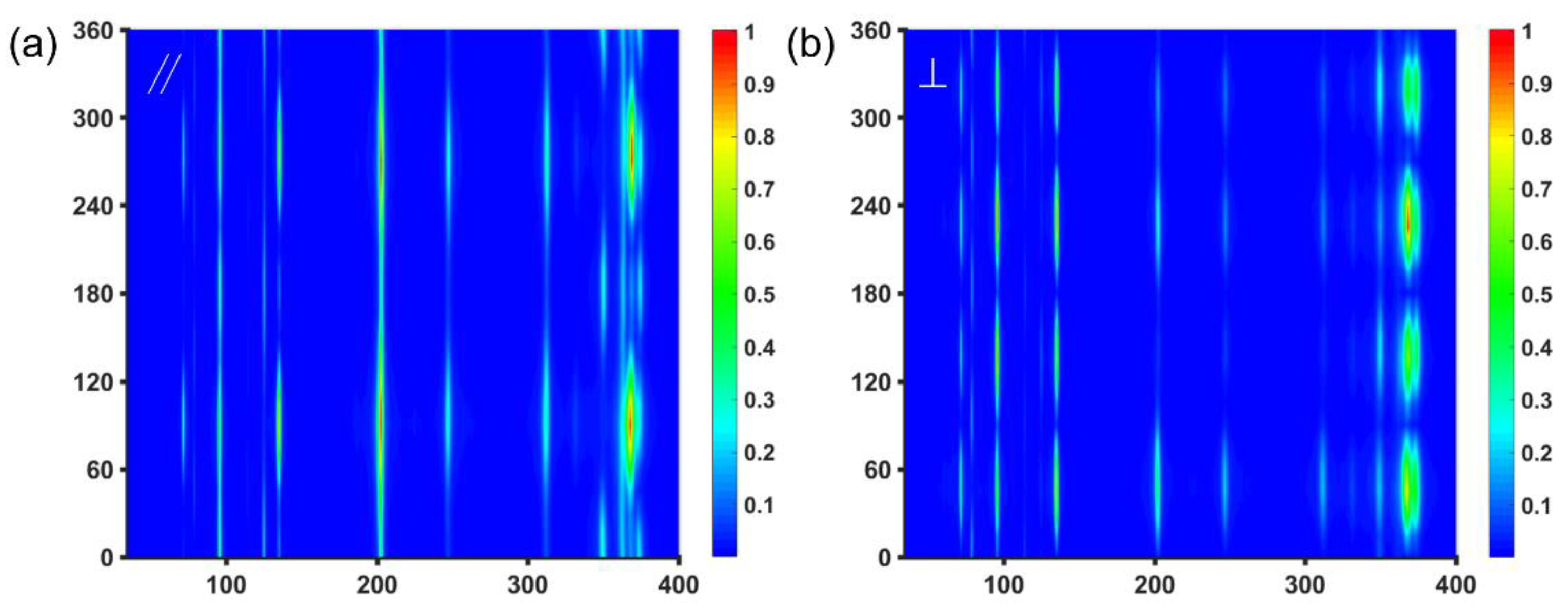
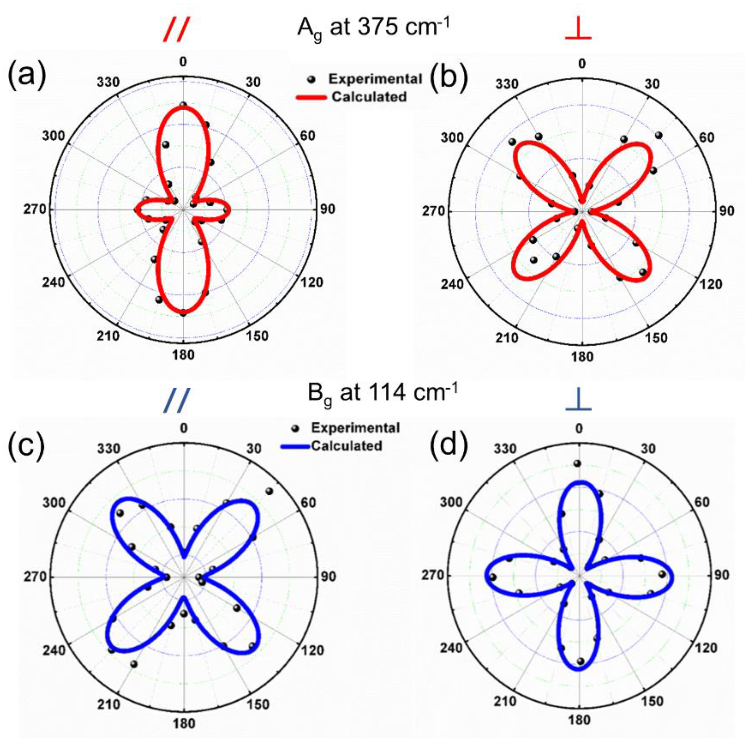
2.3. ARPRS Measurements

The ARPRS measurements were performed using a LabRAM HR Evolution system with a 633 nm laser as excitation source with the parallel and cross backscattering configurations. The incident laser beam was polarized, and the scattering light with polarization was either parallel or perpendicular to the incident polarization. The polarizer in the beam path fixed the polarization direction of the incident laser to the vertical direction, and the directions of the analyzer were set to be vertical or horizontal. The samples were placed on a rotation stage and then the sample was rotated clockwise with an angle θ between the laser polarization direction and the a-axis of the crystal with a step of 15°. The polar plots of anisotropic Raman intensities were obtained by fitting the spectral peaks with the Gaussian–Lorentzian function.

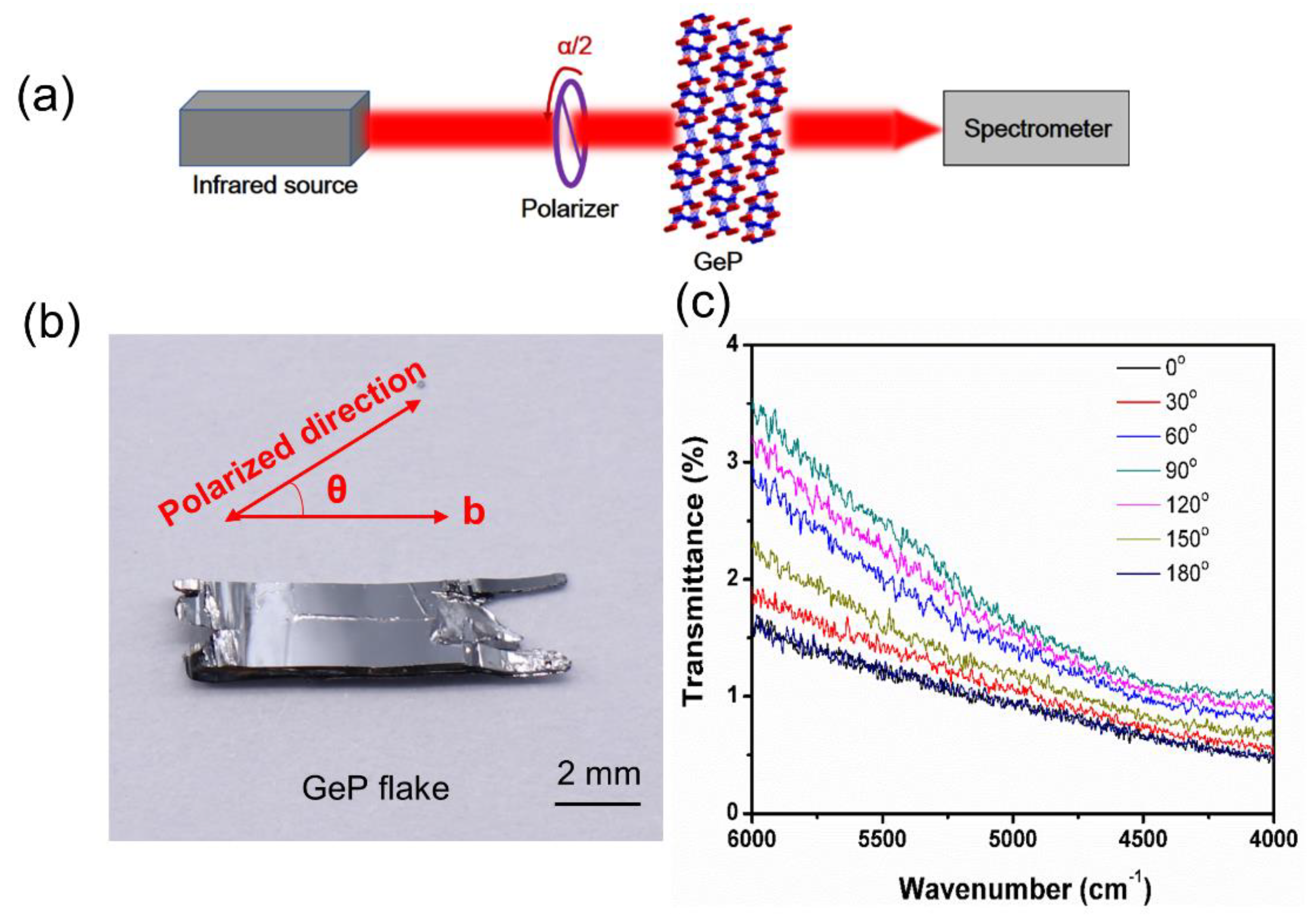
2.4. Transmission Spectra

The infrared polarizer used in this experiment was a Codixx polarized glass polarizer (IR 2000 BC2 HT, Beijing, China). At the wave number range of 4000–6250 cm−1, the transmittance was more than 90%, and the extinction ratio was up to 100:1. By rotating the polarizer to obtain the different polarized light, the in-plane anisotropy of GeP was studied.

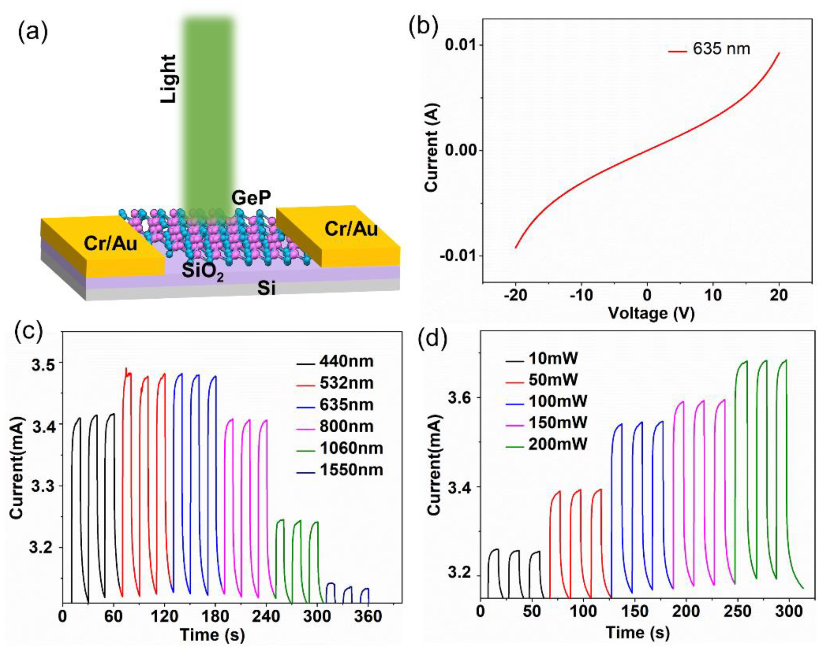
2.5. Photoresponse Measurements

The photodetector based on GeP crystals was fabricated to investigate the photoresponse. The Cr/Au (10/50 nm) electrodes were made by using laser direct writing lithography and followed by electron beam evaporation and lift-off process. The photoelectronic measurements of the fabricated devices were recorded at room using a semiconductor characterization system (4200SCS, Keithley, Solon, OH, USA) on a probe station (CRX-6.5K, Lake Shore, Westerville, OH, USA). The photoresponse of the devices was carried out under the illumination of various lasers (440–1550 nm) with incident power of 10–150 mW. The time-resolved photoresponse curves were measured by switching light at intervals of 10 s.

3. Results and Discussion

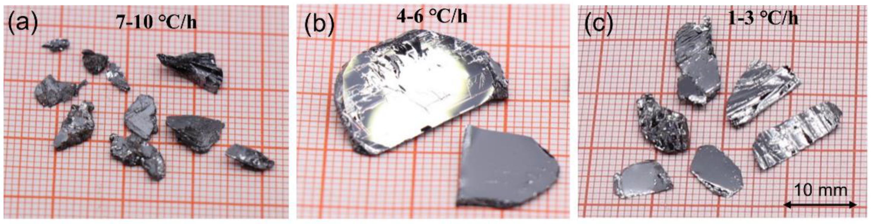
3.1. Bulk GeP Single Crystal Growth

Due to the high melting point of GeP and high vapor pressure of P, the bismuth (Bi) flux method was chosen to grow bulk GeP single crystals. Metallic Bi is a commonly used flux due to its low melting point (210.3 °C) and high boiling point (1564 °C). Additionally, the flux Bi can easily be removed from the grown GeP crystals due to its good solubility in acid. The optimal conditions to produce GeP crystals were as follows: growth temperature 850–900 °C, and raw material composition of Ge:P:Bi was 1:2:4. The cooling rate is an important growth parameter because it affects the morphology and size of GeP crystals. In this work, the cooling rate was selected as 1–10 °C/h.
As shown in Figure 1a–c, the cooling rate of GeP melt has a great effect on the morphology and size. A number of small-sized crystal grains with rough surfaces were obtained at a faster cooling rate of 7–10 °C/h (Figure 1a). When the cooling rate was decreased to 4–6 °C/h, the crystal surfaces of GeP became smooth and shiny, and the size increased to 20 × 15 × 5 mm3, indicating the high crystalline quality of GeP (Figure 1b). When the cooling rate was further decreased to 1–3 °C/h, the size of crystals became smaller (Figure 1c). This result may involve a complicated crystallization process with the competition of nucleation rate and growth velocity of GeP. On the one hand, low cooling rate is favorable for nucleation and crystal growth, but a low cooling rate decreases driving forces for nucleation. Therefore, GeP crystals grown at lower cooling rates have poor quality. On the other hand, although excessive cooling rates provide a large driving force for nucleation to occur, the time needed for the diffusion of atoms may limit nucleation and the growth of crystals. Therefore, GeP crystals grown at higher cooling rates are granular in shape with poor quality. In conclusion, highly crystalline, large-sized GeP crystals can be obtained at a cooling rate of 4–6 °C/h.

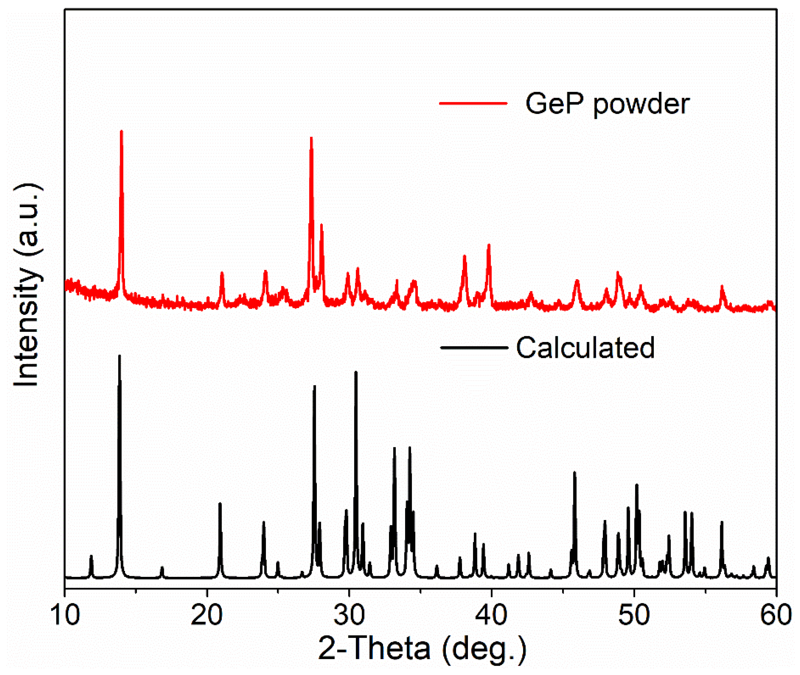
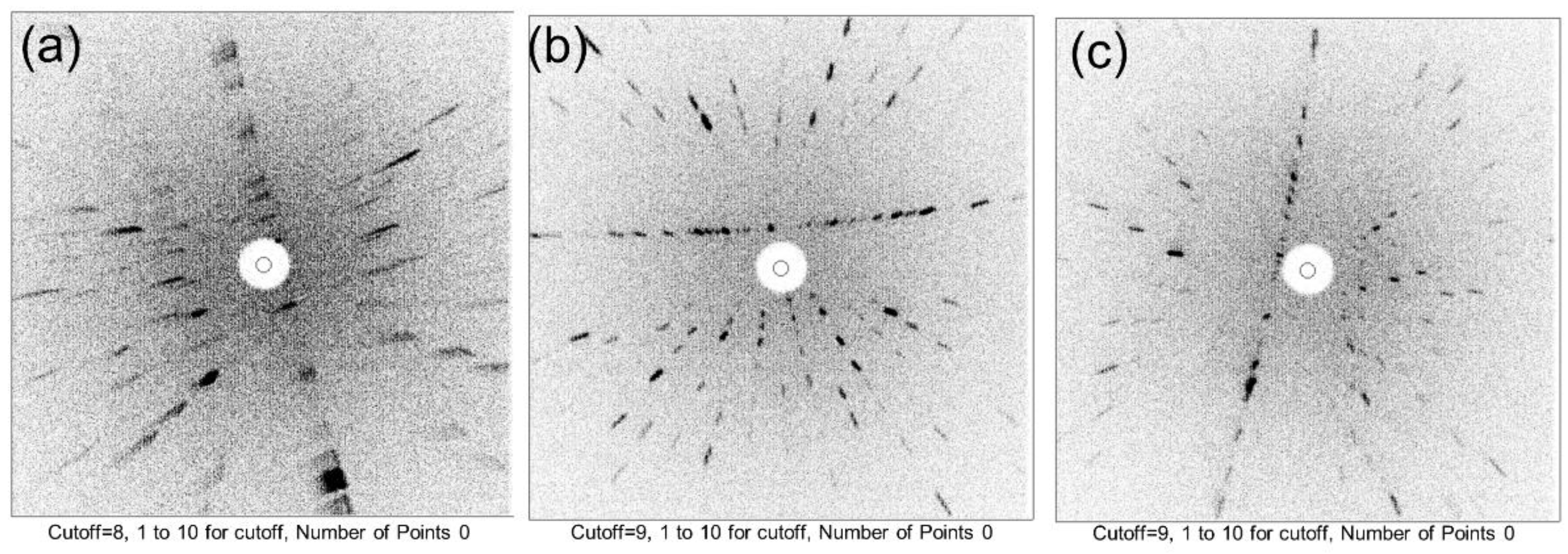
3.2. XRD and Laue Measurements

XRD and Laue measurements were used to characterize the crystalline quality of the grown bulk GeP single crystals. Figure 2 shows the XRD patterns of GeP powder, which was consistent with the theoretically calculated values. The Laue diffraction patterns of GeP crystals grown at different cooling rates are shown in Figure 3. The Laue diffraction patterns in Figure 3b present the clearest and brightest diffraction points for the grown GeP at the cooling rate of 4–6 °C/h, which indicates the highest quality of GeP. Therefore, we can conclude that the cooling rate of 4–6 °C/h might be the optimal growth parameter for large and high-quality bulk GeP single crystals.

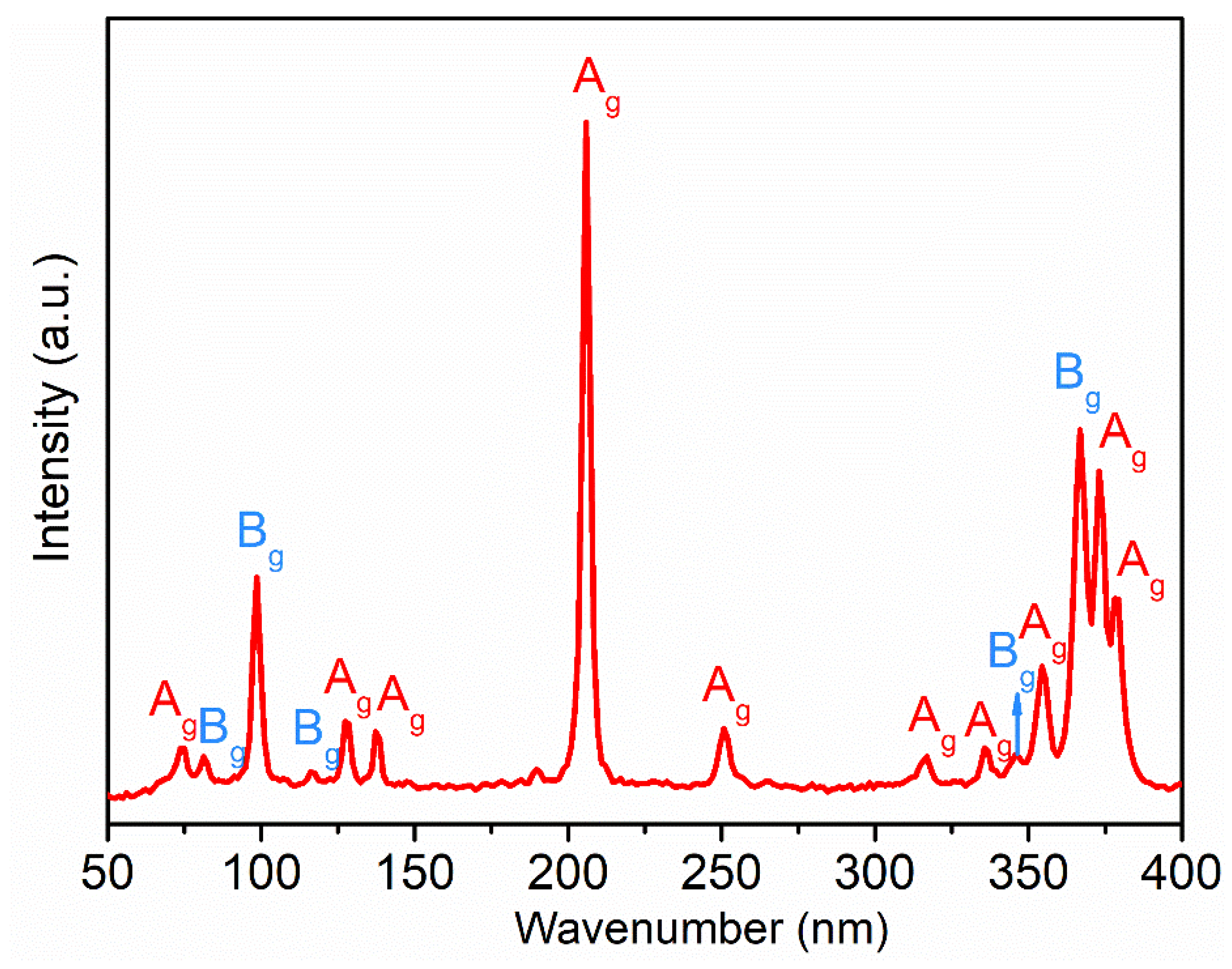
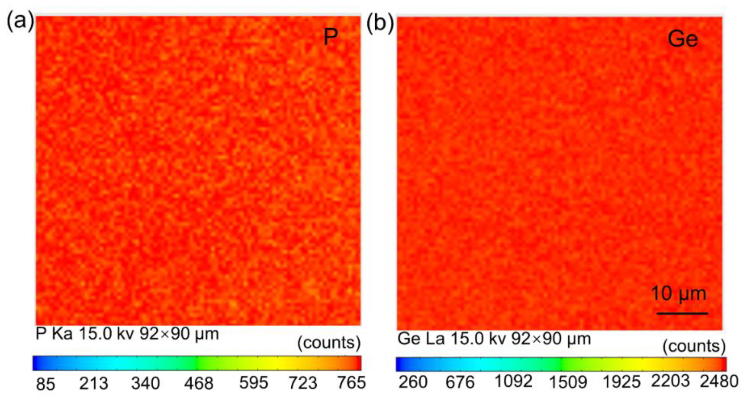
3.3. Raman and EPMA Measurements

The Raman spectrum of GeP bulk crystal is shown in Figure 4, with a 633 nm laser as the excitation source. The Raman spectrum exhibits the sharp and matched peaks, indicating the high quality of the grown GeP crystal, which is in good accordance with the previously reported results [18]. GeP belongs to the C2/m space group; therefore, the irreducible representation of GeP can be expressed as Γoptic = 12Ag + 5Au + 6Bg + 10Bu, where Ag and Bg represent the two typical out-of- and in-plane vibration Raman-active modes of GeP, respectively. The Ge and P elemental distributions of the grown GeP were measured by EPMA, as shown in Figure 5. The results indicate that the elements of Ge and P were relatively evenly distributed in the GeP crystal. The contents of Ge and P were measured to be 50.3% and 49.7%, respectively (Table 1). This elemental ratio matched well with the stoichiometry of GeP. It also proves that there was no excess Bi flux in the GeP crystal.

3.4. Anisotropic Optical Properties

In order to investigate low-symmetry crystal structure and the anisotropic vibrational properties of GeP, the angle-resolved polarized Raman spectra were employed. The phonon vibrations of GeP were considered to be anisotropic due to its low-symmetry monoclinic structure [22]. Here, we studied the anisotropic phonon vibrations of GeP by ARPRS. The normalized polarized scattering intensities evolving at the rotation angle from 0° to 360° are plotted in the false-color image shown in Figure 6a,b. The results display a periodical feature with two-lobed and four-lobed shapes under parallel and perpendicular configurations, which confirmed the strong anisotropy of Raman intensity. Angle dependence of the Raman intensities of GeP was fitted by the formula [18], as shown in Figure 7. The intensity anisotropies of the Ag and Bg modes are exhibited in polar coordinates. We mainly focused on the Raman peaks at 375 cm−1 and 114 cm−1 due to their relatively high intensities. The black dots represent the experimental data points, and the solid lines in red or blue represent the fitted curves. The polar diagrams of Ag and Bg modes both show the petal shapes, which clearly reveals that the polarized Raman spectra are strongly crystalline orientation-dependent.
To further understand the anisotropic optical property of GeP, we investigated the transmission anisotropy of GeP. As is presented in Figure 8a, the incident light was set to pass through the polarizer, which can change partial-polarization light to linear-polarization light and control the direction of linear-polarization light. Figure 8b exhibits the crystallographic b-axis of GeP, corresponding to 0°. As shown in Figure 8c, angle-dependent transmission spectra of GeP flakes were obtained by shifting the polarizing angles from 0° (light polarized along b-axis) to 180° in the range of 6000–4000 cm−1. It is displayed that when the polarization direction was parallel to the b-axis, it showed the lowest transmittance. When the polarization direction was perpendicular to the b-axis, it showed the highest transmittance. Large anisotropy of transmission was displayed to verify the intrinsic optical anisotropy of GeP.

3.5. Photoresponse Performance

To investigate the photoelectric performance of GeP, a photodetector based on GeP was fabricated, as shown in Figure 9a. The transfer characteristics curve with applied voltage ranging from −20 to 20 V under 635 nm laser illumination is exhibited in Figure 9b, which demonstrates satisfactory Ohmic contact between the GeP crystal and Cr/Au electrodes. The photodetectors based on GeP present a broad-band photoresponse under different illumination wavelengths from 440 to 1550 nm at room temperature, as shown in Figure 9c. To further characterize the photocurrent of the GeP based photodetector, the photoresponses under different power were measured under the excitation wavelength of 635 nm. The photocurrent increases with increasing incident power from 10 to 200 mW, as presented in Figure 9d. This phenomenon was also observed in MoS2 and BP [30,31], which could be due to a decrease in photogenerated carriers available for extraction under high photon flux [32].

4. Conclusions

In summary, high-quality and large-sized bulk GeP single crystals with a size of 20 × 15 × 5 mm3 were successfully grown by the flux growth method. The morphology and size of the GeP crystal can be controlled by adjusting the cooling rate during crystal growth. The grown GeP crystals exhibited excellent crystalline quality. The highly anisotropic optical properties were demonstrated by ARPRS and transmission spectra. Furthermore, the photodetectors based on GeP present high performance with a relatively high photocurrent over 3 mA. Our experimental results indicate that GeP might be a promising anisotropic 2D material for optoelectronic applications.

Author Contributions

Conceptualization, S.Z. and S.W. (Shanpeng Wang); methodology, S.Z. and T.Y.; validation, S.Z.; formal analysis, S.Z. and Z.W.; investigation, S.Z., S.W. (Shilei Wang), X.C., and L.W.; data curation, S.Z.; writing—original draft preparation, S.Z.; writing—review and editing, S.Z., T.Y. and S.W. (Shilei Wang); project administration, S.W. (Shanpeng Wang); funding acquisition, S.W. (Shanpeng Wang). All authors have read and agreed to the published version of the manuscript.

Funding

This research was funded by the National Key Research and Development Program of China (Grant No. 2016YFB1102201, 2018YFB0406502), the National Natural Science Foundation of China (51572155, 51932004, and 61975098), and Financial Support from Qilu Young Scholar, the 111 Project 2.0 (Grant No: BP2018013).

Institutional Review Board Statement

Not applicable.

Informed Consent Statement

Not applicable.

Data Availability Statement

Not applicable.

Conflicts of Interest

The authors declare no conflict of interest.

References

  1. Sensale-Rodriguez, B.; Yan, R.; Kelly, M.M.; Fang, T.; Tahy, K.; Hwang, W.S.; Jena, D.; Liu, L.; Xing, H.G. Broadband graphene terahertz modulators enabled by intraband transitions. Nat. Commun. 2012, 3, 780–787. [Google Scholar] [CrossRef] [PubMed]
  2. Jiang, T.; Huang, D.; Cheng, J.; Fan, X.; Zhang, Z.; Shan, Y.; Yi, Y.; Dai, Y.; Shi, L.; Liu, K.; et al. Author Correction: Gate-tunable third-order nonlinear optical response of massless Dirac fermions in graphene. Nat. Photonics 2018, 12, 634. [Google Scholar] [CrossRef] [Green Version]
  3. Jiang, Y.; Mao, J.; Moldovan, D.; Masir, M.R.; Li, G.; Watanabe, K.; Taniguchi, T.; Peeters, F.M.; Andrei, E.Y. Tuning a circular p-n junction in graphene from quantum confinement to optical guiding. Nat. Nanotechnol. 2017, 12, 1045–1049. [Google Scholar] [CrossRef] [PubMed]
  4. Shen, T.Z.; Hong, S.H.; Song, J.K. Electro-optical switching of graphene oxide liquid crystals with an extremely large Kerr coefficient. Nat. Mater. 2014, 13, 394–399. [Google Scholar] [CrossRef]
  5. Wang, X.; Cheng, Z.; Xu, K.; Tsang, H.K.; Xu, J.-B. High-responsivity graphene/silicon-heterostructure waveguide photodetectors. Nat. Photonics 2013, 7, 888–891. [Google Scholar] [CrossRef]
  6. Martinez, A.; Sun, Z. Nanotube and graphene saturable absorbers for fibre lasers. Nat. Photonics 2013, 7, 842–845. [Google Scholar] [CrossRef]
  7. Geim, A.K. Graphene: Status and Prospects. Science 2009, 324, 1530–1534. [Google Scholar] [CrossRef] [PubMed] [Green Version]
  8. Bao, Q.; Kian, P. Graphene Photonics, Plasmonics, and Broadband Optoelectronic Devices. ACS Nano 2012, 6, 3677–3694. [Google Scholar] [CrossRef]
  9. Bonaccorso, F.; Sun, Z.; Hasan, T.; Ferrari, A.C. Graphene photonics and optoelectronics. Nat. Photonics 2010, 4, 611–622. [Google Scholar] [CrossRef] [Green Version]
  10. Liu, X.; Ryder, C.R.; Wells, S.A.; Hersam, M.C. Resolving the In-Plane Anisotropic Properties of Black Phosphorus. Small Methods 2017, 1, 0143–0152. [Google Scholar] [CrossRef]
  11. Liu, H.; Du, Y.; Deng, Y.; Ye, P.D. Semiconducting black phosphorus: Synthesis, transport properties and electronic applications. Chem. Soc. Rev. 2015, 44, 2732–2743. [Google Scholar] [CrossRef] [Green Version]
  12. Xia, F.; Wang, H.; Jia, Y. Rediscovering black phosphorus as an anisotropic layered material for optoelectronics and electronics. Nat. Commun. 2014, 5, 4458–5458. [Google Scholar] [CrossRef] [PubMed] [Green Version]
  13. Sang, D.K.; Wang, H.; Guo, Z.; Xie, N.; Zhang, H. Recent Developments in Stability and Passivation Techniques of Phosphorene toward Next-Generation Device Applications. Adv. Funct. Mater. 2019, 10, 3419–3441. [Google Scholar] [CrossRef]
  14. Lee, B.C.; Kim, C.M.; Jang, H.K.; Lee, J.W.; Joo, M.-K.; Kim, G.-T. Degradation pattern of black phosphorus multilayer field−effect transistors in ambient conditions: Strategy for contact resistance engineering in BP transistors. Appl. Surf. Sci. 2017, 419, 637–641. [Google Scholar] [CrossRef]
  15. Li, C.; Wang, S.; Li, C.; Yu, T.; Jia, N.; Qiao, J.; Zhu, M.; Liu, D.; Tao, X. Highly sensitive detection of polarized light using a new group IV-V 2D orthorhombic SiP. J. Mater. Chem. C 2018, 6, 7219–7225. [Google Scholar] [CrossRef]
  16. Li, L.; Gong, P.; Sheng, D.; Wang, S.; Wang, W.; Zhu, X.; Shi, X.; Wang, F.; Han, W.; Yang, S.; et al. Highly In-Plane Anisotropic 2D GeAs2 for Polarization-Sensitive Photodetection. Adv. Mater. 2018, 10, 4541–4550. [Google Scholar] [CrossRef]
  17. Yang, S.; Yang, Y.; Wu, M.; Hu, C.; Shen, W.; Gong, Y.; Huang, L.; Jiang, C.; Zhang, Y.; Ajayan, P.M. Highly In-Plane Optical and Electrical Anisotropy of 2D Germanium Arsenide. Adv. Funct. Mater. 2018, 28, 1707379. [Google Scholar] [CrossRef]
  18. Li, L.; Wang, W.; Gong, P.; Zhu, X.; Deng, B.; Shi, X.; Gao, G.; Li, H.; Zhai, T. 2D GeP: An Unexploited Low-Symmetry Semiconductor with Strong In-Plane Anisotropy. Adv. Mater. 2018, 30, 6771–6780. [Google Scholar] [CrossRef]
  19. Guo, J.; Liu, Y.; Ma, Y.; Zhu, E.; Lee, S.; Lu, Z.; Zhao, Z.; Xu, C.; Lee, S.J.; Wu, H.; et al. Few-Layer GeAs Field-Effect Transistors and Infrared Photodetectors. Adv. Mater. 2018, 30, 5934–5940. [Google Scholar] [CrossRef]
  20. Zhou, Z.; Long, M.; Pan, L.; Wang, X.; Zhong, M.; Blei, M.; Wang, J.; Fang, J.; Tongay, S.; Hu, W.; et al. Perpendicular Optical Reversal of the Linear Dichroism and Polarized Photodetection in 2D GeAs. ACS Nano 2018, 10, 2269–2279. [Google Scholar] [CrossRef]
  21. Zhang, S.; Guo, S.; Huang, Y.; Zhu, Z.; Cai, B.; Xie, M.; Zhou, W.; Zeng, H. Two-dimensional SiP: An unexplored direct band-gap semiconductor. 2D Mater. 2016, 4, 1833–1838. [Google Scholar] [CrossRef]
  22. Lee, K.; Synnestvedt, S.; Bellard, M. GeP and (Ge1 − xSnx)(P1 − yGey) (x ≈ 0.12, y ≈ 0.05): Synthesis, structure, and properties of two-dimensional layered tetrel phosphides. J. Solid State Chem. 2015, 224, 0022–4596. [Google Scholar] [CrossRef] [Green Version]
  23. Shi, L.-B.; Cao, S.; Yang, M. Strain behavior and Carrier mobility for novel two-dimensional semiconductor of GeP: First principles calculations. Phys. E 2019, 107, 124–130. [Google Scholar] [CrossRef]
  24. Yu, T.; Nie, H.; Wang, S.; Zhang, B.; Zhao, S.; Wang, Z.; Qiao, J.; Han, B.; He, J.; Tao, X. Two-Dimensional GeP-Based Broad-Band Optical Switches and Photodetectors. Adv. Opt. Mater. 2019, 8, 1490–1499. [Google Scholar] [CrossRef]
  25. Guo, J.; Huang, D.; Zhang, Y.; Yao, H.; Wang, Y.; Zhang, F.; Wang, R.; Ge, Y.; Song, Y.; Guo, Z.; et al. 2D GeP as a Novel Broadband Nonlinear Optical Material for Ultrafast Photonics. Laser Photonics Rev. 2019, 13, 0123–0133. [Google Scholar] [CrossRef]
  26. Kim, D.; Park, K.; Shojaei, F.; Debela, T.T.; Kwon, I.S.; Kwak, I.H.; Seo, J.; Ahn, J.P.; Park, J.; Kang, H.S. Thickness-dependent bandgap and electrical properties of GeP nanosheets. J. Mater. Chem. A 2019, 7, 16526–16532. [Google Scholar] [CrossRef]
  27. Shen, H.; Ma, Z.; Yang, B.; Guo, B.; Lyu, Y.; Wang, P.; Yang, H.; Li, Q.; Wang, H.; Liu, Z.; et al. Sodium storage mechanism and electrochemical performance of layered GeP as anode for sodium ion batteries. J. Power Sources 2019, 433, 6682–6690. [Google Scholar] [CrossRef]
  28. Li, W.; Li, X.; Yu, J.; Liao, J.; Zhao, B.; Huang, L.; Ali, A.; Zhang, H.; Wang, J.H.; Guo, Z.; et al. A self-healing layered GeP anode for high-performance Li-ion batteries enabled by low formation energy. Nano Energy 2019, 61, 594–603. [Google Scholar] [CrossRef]
  29. Barreteau, C.; Michon, B.; Besnard, C.; Giannini, E. High-pressure melt growth and transport properties of SiP, SiAs, GeP, and GeAs 2D layered semiconductors. J. Cryst. Growth 2016, 443, 75–80. [Google Scholar] [CrossRef] [Green Version]
  30. Voiry, D.; Salehi, M.; Silva, R.; Fujita, T.; Chen, M.; Asefa, T.; Shenoy, V.B.; Eda, G.; Chhowalla, M. Conducting MoS2 nanosheets as catalysts for hydrogen evolution reaction. Nano Lett. 2013, 13, 6222–6227. [Google Scholar] [CrossRef] [PubMed]
  31. Lopez-Sanchez, O.; Lembke, D.; Kayci, M.; Radenovic, A.; Kis, A. Ultrasensitive photodetectors based on monolayer MoS2. Nat. Nanotechnol. 2013, 8, 497–501. [Google Scholar] [CrossRef] [PubMed]
  32. Buscema, M.; Groenendijk, D.J.; Blanter, S.I.; Steele, G.A.; van der Zant, H.S.; Castellanos-Gomez, A. Fast and broadband photoresponse of few-layer black phosphorus field-effect transistors. Nano Lett. 2014, 14, 3347–3352. [Google Scholar] [CrossRef] [PubMed] [Green Version]
Figure 1. GeP crystals grown by Bi flux method at a cooling rate of (a) 7–10, (b) 4–6 and (c) 1–3 °C/h. Each small square in all images is 1 mm2.
Crystals 11 00235 g001
Figure 2. XRD patterns of GeP powder and the calculated values.
Crystals 11 00235 g002
Figure 3. Laue patterns of bulk GeP single crystals grown by Bi flux method at a cooling rate of (a) 7–10 °C/h, (b) 4–6 °C/h and (c) 1–3 °C/h.
Crystals 11 00235 g003
Figure 4. Raman spectrum of GeP crystal marked with Ag and Bg Raman modes.
Crystals 11 00235 g004
Figure 5. The elemental mapping images of Ge (a) and P (b) measured by electron probe microanalysis (EPMA).
Crystals 11 00235 g005
Figure 6. False-color plots of polarized Raman intensities under parallel (a) and perpendicular (b) polarization configurations.
Crystals 11 00235 g006
Figure 7. The anisotropic Raman intensities in polar coordinates under parallel and perpendicular polarization configurations for (a,b) Ag mode at 375 cm−1 and (c,d) Bg mode at 114 cm−1, respectively.
Crystals 11 00235 g007
Figure 8. (a) Schematic diagram of angle-resolved spectrometer for anisotropic transmission measurements. (b) Photograph of GeP flake with schematic angle between polarized direction and crystallographic b-axis. (c) Infrared transmittance spectra of GeP at different polarization directions.
Crystals 11 00235 g008
Figure 9. (a) Schematic of GeP photodetector. (b) Current–voltage (I–V) curve under 635 nm incident light. (c) Time-resolved photocurrent of the GeP photodetector under 440–1550 nm incident light. (d) Time-resolved photocurrent of the GeP photodetector under different incident power for 635 nm incident light.
Crystals 11 00235 g009
Table 1. The elemental contents of Ge and P.
ElementNormalized Mass (%)Mol (%)
Ge70.35350.312
P29.64749.688
Total100.000100.000
Publisher’s Note: MDPI stays neutral with regard to jurisdictional claims in published maps and institutional affiliations.

